MPSH11 / MMBTH11
Discrete POWER & Signal Technologies
MPSH11
MMBTH11
C
E C BE
TO-92 SOT-23
Mark: 3G
B
NPN RF Transistor
This device is designed for common-emitter low noise amplifier and mixer applications with collector currents in the 100 µA to 10 mA range to 300 MHz, and low frequency drift common-base VHF oscillator applications with high output levels for driving FET mixers. Sourced from Process 47.
Absolute Maximum Ratings*
Symbol
VCEO VCBO VEBO IC TJ, Tstg Collector-Emitter Voltage Collector-Base Voltage Emitter-Base Voltage Collector Current - Continuous
TA = 25°C unless otherwise noted
Parameter
Value
25 30 3.0 50 -55 to +150
Units
V V V mA °C
Operating and Storage Junction Temperature Range
*These ratings are limiting values above which the serviceability of any semiconductor device may be impaired.
NOTES: 1) These ratings are based on a maximum junction temperature of 150 degrees C. 2) These are steady state limits. The factory should be consulted on applications involving pulsed or low duty cycle operations.
Thermal Characteristics
Symbol
PD RθJC RθJA
TA = 25°C unless otherwise noted
Characteristic
Total Device Dissipation Derate above 25°C Thermal Resistance, Junction to Case Thermal Resistance, Junction to Ambient MPSH11 350 2.8 125 357
Max
*MMBTH11 225 1.8 556
Units
mW mW/ °C °C/W °C/W
*Device mounted on FR-4 PCB 1.6" X 1.6" X 0.06."
©1997 Fairchild Semiconductor Corporation
�MPSH11 / MMBTH11
NPN RF Transistor
(continued)
Electrical Characteristics
Symbol Parameter
TA = 25°C unless otherwise noted
Test Conditions
Min
Max
Units
OFF CHARACTERISTICS
V(BR)CEO V(BR)CBO V(BR)EBO ICBO IEBO Collector-Emitter Sustaining Voltage* Collector-Base Breakdown Voltage Emitter-Base Breakdown Voltage Collector Cutoff Current Emitter Cutoff Current I C = 1.0 mA, IB = 0 I C = 100 µA, I E = 0 I E = 10 µA, I C = 0 VCB = 25 V, IE = 0 VEB = 2.0 V, IC = 0 25 30 3.0 100 100 V V V nA nA
ON CHARACTERISTICS
hFE VCE(sat ) VBE( on) DC Current Gain Collector-Emitter Saturation Voltage Base-Emitter On Voltage I C = 4.0 mA, VCE = 10 V I C = 4.0 mA, IB = 0.4 mA I C = 4.0 mA, VCE = 10 V 60 0.5 0.95 V V
SMALL SIGNAL CHARACTERISTICS
fT Ccb Crb rb’Cc Current Gain - Bandwidth Product Collector-Base Capacitance Collector Base Time Constant I C = 4.0 mA, VCE = 10 V, f = 100 MHz VCB = 10 V, IE = 0, f = 1.0 MHz I C = 4.0 mA, VCB = 10 V, f = 31.8 MHz 650 0.7 0.6 0.9 9.0 MHz pF pF pS
Common-Base Feedback Capacitance VCB = 10 V, IE = 0, f = 1.0 MHz
*Pulse Test: Pulse Width ≤ 300 µs, Duty Cycle ≤ 2.0%
DC Typical Characteristics
300 VCE = 5V 250
1 25 ºC
VCESAT- COLLECTOR-EMITTER VOLTAGE (V)
DC Current Gain vs Collector Current
h FE - DC PULSED CURRENT GAIN
Collector-Emitter Saturation Voltage vs Collector Current
0.2 β = 10 0.15
125 ºC
200 150 100 50 0 0.01 0.1 1 10 I C- COLLECTOR CURRENT (mA)
P4
25 °C
0.1
25 °C
- 4 0 ºC
0.05
- 40 ºC
100
0.1
1 10 I C - COLLECTOR CURRENT (mA)
P4
20 30
�MPSH11 / MMBTH11
NPN RF Transistor
(continued)
DC Typical Characteristics
Base-Emitter Saturation Voltage vs Collector Current
1 0.8 0.6 0.4 0.2 0.1 1 10 I C - COLLECTOR CURRENT (mA)
P 47
(continued)
VBE(ON) BASE-EMITTER ON VOLTAGE (V) -
VBESAT- BASE-EMITTER VOLTAGE (V)
Base-Emitter ON Voltage vs Collector Current
1
- 40 ºC
- 40 ºC 25 °C 125 ºC
0.8
25 °C
0.6
125 ºC
β = 10
0.4
V CE = 5V
0.1 1 10 I C - COLLECTOR CURRENT (mA)
P4
20 30
0.2 0.01
100
Collector-Cutoff Current vs Ambient Temperature
ICBO- COLLECTOR CURRENT (nA) 10 VCB= 30V 1
0.1
25
50 75 100 125 T A - AMBIENT TEMPERATURE ( º C)
P4
150
AC Typical Characteristics
Capacitance vs. Reverse Bias Voltage Contours of Constant Gain Bandwidth Product (fT)
�MPSH11 / MMBTH11
NPN RF Transistor
(continued)
Common Emitter Y Parameters
Input Admittance vs. Collector Current Input Admittance vs. Collector Current
Input Admittance vs. Collector Voltage
Input Admittance vs. Frequency
Forward Transfer Admittance vs. Collector Current
Forward Transfer Admittance vs. Collector Current
�MPSH11 / MMBTH11
NPN RF Transistor
(continued)
Common Emitter Y Parameters
Forward Transfer Admittance vs. Collector Voltage
(continued)
Forward Transfer Admittance vs. Frequency
Reverse Transfer Admittance vs. Collector Current
Reverse Transfer Admittance vs. Collector Current
Reverse Transfer Admittance vs. Collector Voltage
Reverse Transfer Admittance vs. Frequency
�MPSH11 / MMBTH11
NPN RF Transistor
(continued)
Common Emitter Y Parameters
Output Admittance vs. Collector Current
(continued)
Output Admittance vs. Collector Current
Output Admittance vs. Collector Voltage
Output Admittance vs. Frequency
Power Gain and Noise Figure vs. Collector Current
Conversion Gain vs. Collector Current
�MPSH11 / MMBTH11
NPN RF Transistor
(continued)
AC Typical Characteristics
POWER DISSIPATION vs AMBIENT TEMPERATURE
P D - POWER DISSIPATION (mW) 350 300 250 200 150 100 50 0 0 25 50 75 100 TEMPERATURE ( ° C) 125 150
TO-92 SOT-23
Test Circuits
VCC = 12 V 270 Ω
1000 pF
1000 pF L2 RL 100 pF 200 mHz Input 0.8-10 pF L1 RS 200 mHz Output into 50Ω
1000 pF
1000 pF
390 Ω L1 - Ohmite Z-235 RFC L2 - L6 turns No. 14 wire, 1 inch L x 1/4 inch ID tapped 1 1/2 turns from cold side
2.2 K Ω
VBB
FIGURE 1: Unneutralized 200 MHz PG NF Test Circuit
�MPSH11 / MMBTH11
NPN RF Transistor
(continued)
Test Circuits
(continued)
T1 0.002 µF 50 Ω Input 2.2 K Ω 1/2 W 1000 pF 4.0-30 pF 2KΩ 50 Ω Output
1000 pF
1000 pF 390 Ω 1/2 W
270 Ω 1/2 W
R.F. Beads VCC = 12 V VAGC
T1 - Q3 Toroid 4:1 ratio 8 turns Pri. 2 turns Sec.
}
No. 22 wire
FIGURE 2: 45 MHz Power Gain Circuit
200 mHz Output into 50Ω RFin 1.1 pF 2.0 pF LOin 245 mHz Output into 50 Ω 47 KΩ L1 - Ohmite RFC Z235 T1 - Primary 5 turns No. 34 wire 1/4 inch diameter. Secondary runs No. 34 wire closer wound over a Q100 core (10.7 mHz). When terminated onm secondary side with 50Ω primary measures 1.5 K, -25 pF. L1 1000 pF 1000 pF 20pF 45 mHz Output into 50Ω
300 pF
T1
VBB
VCE VCE = 15 V
FIGURE 3: 200 MHz Conversion Gain Test Circuit
�
很抱歉,暂时无法提供与“MMBTH11”相匹配的价格&库存,您可以联系我们找货
免费人工找货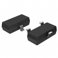


 工商网监
湘ICP备2023018690号
工商网监
湘ICP备2023018690号
