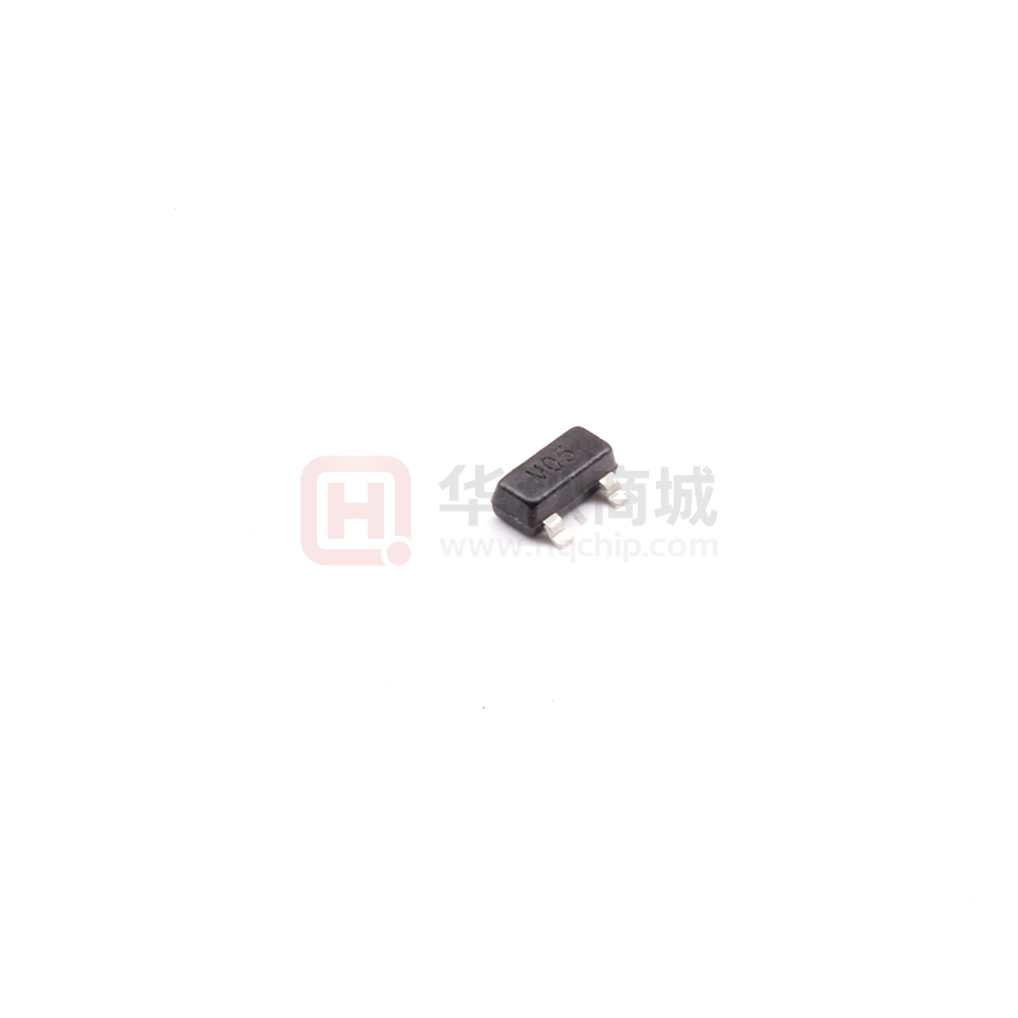
SM05 through SM36
TVS Diode Array
PROTECTION PRODUCTS
Description
Features
The SM series of transient voltage suppressors (TVS)
are designed to protect components which are
connected to data and transmission lines from voltage
surges caused by electrostatic discharge (ESD),
electrical fast transients (EFT), and lightning.
300 watts peak pulse power (tp = 8/20μs)
Transient protection for data & power lines to
TVS diodes are characterized by their high surge
capability, low operating and clamping voltages, and
fast response time. This makes them ideal for use as
board level protection of sensitive semiconductor
components. The dual-junction common-anode design
allows the user to protect one bidirectional data line or
two unidirectional lines. The low profile SOT23
package allows flexibility in the design of “crowded”
circuit boards.
IEC 61000-4-2 (ESD) ±15kV (air), ±8kV (contact)
IEC 61000-4-4 (EFT) 40A (5/50ns)
IEC 61000-4-5 (Lightning) 12A (8/20μs)
Protects one bidirectional line or two unidirectional
lines
Working Voltages: 5V, 12V, 15V, 24V and 36V
Low clamping voltage
Solid-state silicon avalanche technology
Mechanical Characteristics
The SM series may be used to meet the ESD immunity
requirements of IEC 61000-4-2, Level 4, “Human Body
Model” for air and contact discharge.
JEDEC SOT-23 package
Molding compound flammability rating: UL 94V-0
Marking : Marking Code
Packaging : Tape and Reel
Lead Finish: Matte tin
RoHS/WEEE Compliant
Applications
Circuit Diagram
Cellular Handsets and Accessories
Portable Electronics
Industrial Controls
Set-Top Box
Servers, Notebook, and Desktop PC
Schematic & PIN Configuration
SOT-23 (Top View)
Revision 05/26/09
1
www.semtech.com
�SM05 through SM36
PROTECTION PRODUCTS
Absolute Maximum Rating
R ating
Symbol
Value
Units
Peak Pulse Power (tp = 8/20μs)
Pp k
300
Watts
Thermal Resistance, Junction to Ambient
θJ A
556
°C/W
Lead Soldering Temp erature
TL
260 (10 sec.)
°C
Op erating Temp erature
TJ
-55 to +125
°C
TSTG
-55 to +150
°C
Storage Temp erature
Electrical Characteristics
SM05
Par ame te r
Symbo l
Co nditio ns
Minimum
Typical
Maximum
Units
5
V
Reverse Stand-Off Voltage
VRWM
Reverse Breakdown Voltage
V BR
It = 1mA
Reverse Leakage Current
IR
VRWM = 5V, T=25°C
20
μA
Clamp ing Voltage
VC
IPP = 1A,
tp = 8/20μs
9.8
V
Peak Pulse Current
IP P
tp = 8/20μs
17
A
Junction Cap acitance
Cj
Pi n 1 to 2
VR = 0V, f = 1MHz
350
pF
Junction Cap acitance
Cj
Pin 1 to 3 and
Pi n 2 to 3
VR = 0V, f = 1MHz
400
pF
Symbo l
Co nditio ns
Maximum
Units
12
V
6
V
SM12
Par ame te r
Minimum
Typical
Reverse Stand-Off Voltage
VRWM
Reverse Breakdown Voltage
V BR
It = 1mA
Reverse Leakage Current
IR
VRWM = 12V, T=25°C
1
μA
Clamp ing Voltage
VC
IPP = 1A,
tp = 8/20μs
19
V
Peak Pulse Current
IP P
tp = 8/20μs
12
A
Junction Cap acitance
Cj
Pi n 1 to 2
VR = 0V, f = 1MHz
120
pF
Junction Cap acitance
Cj
Pin 1 to 3 and
Pi n 2 to 3
VR = 0V, f = 1MHz
150
pF
© 2009 Semtech Corp.
2
13.3
V
www.semtech.com
�SM05 through SM36
PROTECTION PRODUCTS
Electrical Characteristics (Continued)
SM15
Parameter
Symbol
Conditions
Minimum
Typical
Maximum
Units
15
V
Reverse Stand-Off Voltage
VRWM
Reverse Breakdown Voltage
V BR
It = 1mA
Reverse Leakage Current
IR
VRWM = 15V, T=25°C
1
μA
Clamp ing Voltage
VC
IPP = 1A, tp = 8/20μs
24
V
Peak Pulse Current
IP P
tp = 8/20μs
10
A
Junction Cap acitance
Cj
Pi n 1 to 2
VR = 0V, f = 1MHz
75
pF
Junction Cap acitance
Cj
Pin 1 to 3 and 2 to 3
VR = 0V, f = 1MHz
100
pF
Symbol
Conditions
Maximum
Units
24
V
16.7
V
SM24
Parameter
Minimum
Typical
Reverse Stand-Off Voltage
VRWM
Reverse Breakdown Voltage
V BR
It = 1mA
Reverse Leakage Current
IR
VRWM = 24V, T=25°C
1
μA
Clamp ing Voltage
VC
IPP = 1A, tp = 8/20μs
43
V
Peak Pulse Current
IP P
tp = 8/20μs
5
A
Junction Cap acitance
Cj
Pi n 1 to 2
VR = 0V, f = 1MHz
50
pF
Junction Cap acitance
Cj
Pin 1 to 3 and 2 to 3
VR = 0V, f = 1MHz
60
pF
Symbol
Conditions
Maximum
Units
36
V
26.7
V
SM36
Parameter
Minimum
Typical
Reverse Stand-Off Voltage
VRWM
Reverse Breakdown Voltage
V BR
It = 1mA
Reverse Leakage Current
IR
VRWM = 36V, T=25°C
1
μA
Clamp ing Voltage
VC
IPP = 1A, tp = 8/20μs
60
V
Peak Pulse Current
IP P
tp = 8/20μs
4
A
Junction Cap acitance
Cj
Pi n 1 to 2
VR = 0V, f = 1MHz
40
pF
Junction Cap acitance
Cj
Pin 1 to 3 and 2 to 3
VR = 0V, f = 1MHz
45
pF
© 2009 Semtech Corp.
3
40
V
www.semtech.com
�SM05 through SM36
PROTECTION PRODUCTS
Typical Characteristics
Non-Repetitive Peak Pulse Power vs. Pulse Time
Power Derating Curve
10
110
Peak Pulse Power - Ppk (kW)
100
% of Rated Power or IPP
90
1
0.1
80
70
60
50
40
30
20
10
0
0.01
0
0.1
1
10
100
25
1000
50
75
100
125
150
o
Ambient Temperature - TA ( C)
Pulse Duration - tp (µs)
Pulse Waveform
110
W aveform
Parameters:
tr = 8µs
td = 20µs
100
90
Percent of IPP
80
70
e -t
60
50
40
td = I PP /2
30
20
10
0
0
5
10
15
20
25
30
T im e (µs)
ESD Pulse Waveform (Per IEC 61000-4-2)
IEC 61000-4-2 Discharge Parameters
Level
© 2009 Semtech Corp.
4
First
Peak
Current
Peak
Current
at 30 ns
Peak
Current
at 60 ns
Test
Test
Voltage
Voltage
(Contact
(A ir
Discharge) Discharge)
( kV )
(kV)
(A )
(A )
(A )
1
7.5
4
8
2
2
2
15
8
4
4
4
3
22.5
12
6
6
8
4
30
16
8
8
15
www.semtech.com
�SM05 through SM36
PROTECTION PRODUCTS
Applications Information
Device Connection Options
Device Schematic & Pin Configuration
The SM series is designed to protect one bidirectional
or two unidirectional data or I/O lines operating at 5 to
36 volts. Connection options are as follows:
z Bidirectional: Pin 1 is connected to the data line
and pin 2 is connected to ground (Since the device
is symmetrical, these connections may be reversed). The ground connection should be made
directly to a ground plane. The path length should
be kept as short as possible to minimize parasitic
inductance. Pin 3 is not connected.
z Unidirectional: Data lines are connected to pin 1
and pin 2. Pin 3 is connected to ground. For best
results, this pin should be connected directly to a
ground plane on the board. The path length should
be kept as short as possible to minimize parasitic
inductance.
RS-232 Transceiver Protection Example
Circuit Board Layout Recommendations for Suppression of ESD.
Good circuit board layout is critical for the suppression
of fast rise-time transients such as ESD. The following
guidelines are recommended (Refer to application note
SI99-01 for more detailed information):
z Place the TVS near the input terminals or connectors to restrict transient coupling.
z Minimize the path length between the TVS and the
protected line.
z Minimize all conductive loops including power and
ground loops.
z The ESD transient return path to ground should be
kept as short as possible.
z Never run critical signals near board edges.
z Use ground planes whenever possible.
Matte Tin Lead Finish
Matte tin has become the industry standard lead-free
replacement for SnPb lead finishes. A matte tin finish
is composed of 100% tin solder with large grains.
Since the solder volume on the leads is small compared to the solder paste volume that is placed on the
land pattern of the PCB, the reflow profile will be
determined by the requirements of the solder paste.
Therefore, these devices are compatible with both
lead-free and SnPb assembly techniques. In addition,
unlike other lead-free compositions, matte tin does not
have any added alloys that can cause degradation of
the solder joint.
© 2009 Semtech Corp.
5
www.semtech.com
�SM05 through SM36
PROTECTION PRODUCTS
Outline Drawing - SOT23
e1
3
DIMENSIONS
MILLIMETERS
MIN NOM MAX
B
DIM
E1
1
A
A1
A2
b
c
D
E1
E
e
e1
L
L1
N
0
aaa
bbb
E
2
bxN
bbb
e
D
C A B
1.20
0.89
0.01
0.10
0.88
1.10
0.30
0.51
0.08
0.18
2.80 2.90 3.04
1.20 1.30 1.40
2.10
2.64
1.90 BSC
0.95 BSC
0.40 0.50 0.60
(0.55)
3
0°
8°
0.10
0.20
A
A2
aaa C
A
SEATING
PLANE
A1
C
H
GAUGE PLANE
SEATING
PLANE
c
0
C
L
L1
0.25
SIDE VIEW
DETAIL A
SEE DETAIL A
NOTES:
1. CONTROLLING DIMENSIONS ARE IN MILLIMETERS (ANGLES IN DEGREES).
2. DATUMS -A- AND -B-
TO BE DETERMINED AT DATUM PLANE -H-
3. DIMENSIONS "E1" AND "D" DO NOT INCLUDE MOLD FLASH, PROTRUSIONS
OR GATE BURRS.
Land Pattern - SOT23
X
DIMENSIONS
DIM MILLIMETERS
(C)
Z
G
Y
C
G
E1
E
X
Y
Z
(2.20)
0.80
0.95
1.90
1.00
1.40
3.60
E1
E
NOTES:
1.
CONTROLLING DIMENSIONS ARE IN MILLIMETERS (ANGLES IN DEGREES).
2. THIS LAND PATTERN IS FOR REFERENCE PURPOSES ONLY
CONSULT YOUR MANUFACTURING GROUP TO ENSURE YOUR
COMPANY'S MANUFACTURING GUIDELINES ARE MET.
3. REFERENCE IPC-SM-782A.
© 2009 Semtech Corp.
6
www.semtech.com
�SM05 through SM36
PROTECTION PRODUCTS
Marking Codes
Ordering Information
Part Number
Marking
Code
Part Number
Qty per
Reel
R eel Size
SM05
M05
SM05.TCT
3,000
7 Inch
SM12
M12
SM12.TCT
3,000
7 Inch
SM15
M15
SM15.TCT
3,000
7 Inch
SM24
M24
SM24.TCT
3,000
7 Inch
SM36
M36
SM36.TCT
3,000
7 Inch
Tape and Reel Specification
Pin 1 Location
User Direction of feed
A0
3.15 +/-0.15 mm
B0
K0
2.77 +/-0.15 mm
Tape
Width
B, (Max)
D
8 mm
4.2 mm
(.165)
1.5 + 0.1 mm
- 0.0 mm
1.22 +/-0.15 mm
D1
E
1.0 mm
±0.05
1.750±.10
mm
F
K
(MAX)
P
P0
P2
T(MAX)
3.5±0.05
mm
2.4 mm
4.0±0.1
mm
4.0±0.1
mm
2.0±0.05
mm
0.4 mm
W
8.0 mm
+ 0.3 mm
- 0.1 mm
Contact Information
Semtech Corporation
Protection Products Division
200 Flynn Road, Camarillo, CA 93012
Phone: (805)498-2111 FAX (805)498-3804
© 2009 Semtech Corp.
7
www.semtech.com
�


 工商网监
湘ICP备2023018690号
工商网监
湘ICP备2023018690号
