Thyristors Datasheet
C122F1G
Surface Mount – 50V
Pb
Description
Designed primarily for full-wave ac control applications, such as
motor controls, heating controls and power supplies; or wherever
half−wave silicon gate−controlled, solid−state devices are
needed.
Features
■ Glass Passivated Junctions
and Center Gate Fire for
Greater Parameter Uniformity
and Stability
■ Blocking Voltage to 50 Volts
■ This is a Pb−Free Device
■ Small, Rugged, Thermowatt
Construction for Low Thermal
Resistance, High Heat
Dissipation and Durability
Additional Information
Functional Diagram
G
K
A
Resources
Accessories
Samples
Pin Out
4
1
1
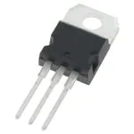
TO-220AB
Case 221A
Style 4
23
© 2021 Littelfuse, Inc.
Specifications are subject to change without notice.
Revised: GD. 02/19/21
�Thyristors Datasheet
C122F1G
Surface Mount – 50V
Maximum Ratings (TJ = 25°C unless otherwise noted)
Rating
Symbol
VDRM,
VRRM
IT (RMS)
ITSM
I2t
PGM
PG (AV)
IGM
TJ
Tstg
Peak Repetitive Off-State Voltage (Note 1)
(Gate Open, Sine Wave 50 to 60 Hz, TJ = 25° to 100°C)
On-State RMS Current (180° Conduction Angles; TC = 75°C)
Peak Non-Repetitive Surge Current (1/2 Cycle, Sine Wave, 60 Hz, TC = 75°C)
Circuit Fusing Consideration (t = 8.3 ms)
Forward Peak Gate Power (Pulse Width = 10 µs, TC = 70°C)
Forward Average Gate Power (t = 8.3 ms, TC = 70°C)
Forward Peak Gate Current (Pulse Width = 10 s, TC = 70°C)
Operating Junction Temperature Range
Storage Temperature Range
Value
Unit
50
V
8.0
90
34
5.0
0.5
2.0
-40 to +125
-40 to +150
A
A
A²sec
W
W
W
°C
°C
Stresses exceeding Maximum Ratings may damage the device. Maximum Ratings are stress ratings only. Functional operation above the Recommended Operating Conditions is not implied. Extended exposure to stresses above the
Recommended Operating Conditions may affect device reliability.
1. VDRM and VRRM for all types can be applied on a continuous basis. Ratings apply for zero or negative gate voltage; however, positive gate voltage shall not be applied concurrent with negative potential on the anode. Blocking voltages
shall not be tested with a constant current source such that the voltage ratings of the devices are exceeded.
Thermal Characteristics
Rating
Symbol
Value
Unit
R8JC
R8JA
1.8
62.5
°C/W
TL
260
°C
Junction−to−Case (AC)
Junction−to−Ambient
Thermal Resistance
Maximum Lead Temperature for Soldering Purposes, 1/8” from case for 10 seconds
Electrical Characteristics - OFF (TC = 25°C unless otherwise noted)
Characteristic
TJ = 25°C
TJ = 125°C
†Peak Repetitive Blocking Current
(VAK = VDRM = VRRM; Gate Open)
Symbol
Min
Typ
Max
IDRM,
IRRM
-
-
10
Unit
µA
-
-
0.5
mA
Electrical Characteristics - ON (TC = 25°C unless otherwise noted; Electricals apply in both
directions)
Characteristic
Peak On−State Voltage (Note 2) (ITM = 16 A Peak, TC = 25°C)
TC = 25°C
Gate Trigger Current (Continuous dc)
(VAK= 12 V, RL = 100 Ω)
TC = -40°C
Gate Trigger Voltage (Continuous dc)
(VAK= 12 V, RL = 100 Ω)
TC = -40°C
TC = 25°C
Gate Non−Trigger Voltage (Continuous dc)
(VAK = 12 V, RL = 100 Ω, TC = 125°C)
Symbol
Min
Typ
Max
Unit
VTM
−
−
1.83
V
−
−
25
−
−
40
−
−
1.5
−
−
2.0
0.2
−
−
−
−
30
−
−
60
−
30
−
IGT
VGT
VGD
TC = 25°C
Holding Current
(VD = 12 V, Gate Open, Initiating Current = 200 mA)
TC = -40°C
Turn-Of f Time (VD = Rated VDRM)
(ITM = 8 A, IR = 8 A)
VGD
tq
mA
V
mA
μS
2. Indicates Pulse Test: Pulse Width ≤ 2.0 ms, Duty Cycle ≤ 2%.
Dynamic Characteristics
Characteristic
Critical Rate of Rise of Off-State Voltage
(VD = 0.66 x VDRM, Exponential Waveform, Gate Open, TJ = 100°C)
2
Symbol
Min
Typ
Max
Unit
dV/dt
−
200
−
V/µs
© 2021 Littelfuse, Inc.
Specifications are subject to change without notice.
Revised: GD. 02/19/21
�Thyristors Datasheet
C122F1G
Surface Mount – 50V
Voltage Current Characteristic of SCR
+Current
Symbol
Parameter
VDRM
Peak Repetitive Forward Off State Voltage
IDRM
Peak Forward Blocking Current
VRRM
Peak Repetitive Reverse Off State Voltage
IRRM
Peak Reverse Blocking Current
VTM
Maximum On State Voltage
IH
Holding Current
VTM
On State
IRRM at VRRM
IH
Quadrant 3
Main Terminal 2-
Quadrant 1
Main Terminal 2+
IH
Off State
+Voltage
IDRM at VDRM
VTM
Figure 1. Current Derating (Half-Wave)
Figure 2. Current Derating (Full-Wave)
Figure 3. Maximum Power Dissipation (Half-Wave)
Figure 4. Maximum Power Dissipation (Full-Wave)
3
© 2021 Littelfuse, Inc.
Specifications are subject to change without notice.
Revised: GD. 02/19/21
�Thyristors Datasheet
C122F1G
Surface Mount – 50V
Dimensions
Part Marking System
SEATING
PLANE
B
F
4
Q
12
C
T
S
4
A
TO-220AB
Case 221A
Style 3
U
3
H
K
Z
1
R
L
V
23
J
G
D
N
Dim
Inches
Millimeters
Y
M
A
AKA
G
YMAXX
C122F1G
AKA
=Year
=Month
=Assembly Site
=Diode Polarity
=Pb-Free Package
Pin Assignment
Min
Max
Min
Max
1
Cathode
A
0.590
0.620
14.99
15.75
2
Anode
B
0.380
0.420
9.65
10.67
3
Gate
4
Anode
C
0.178
0.188
4.52
4.78
D
0.025
0.035
0.64
0.89
F
0.142
0.147
3.61
3.73
G
0.095
0.105
2.41
2.67
H
0.110
0.130
2.79
3.30
J
0.018
0.024
0.46
0.61
K
0.540
0.575
13.72
14.61
L
0.060
0.075
1.52
1.91
N
0.195
0.205
4.95
5.21
Q
0.105
0.115
2.67
2.92
R
0.085
0.095
2.16
2.41
S
0.045
0.060
1.14
1.52
T
0.235
0.255
5.97
6.47
U
0.000
0.050
0.00
1.27
V
0.045
-
1.15
-
Z
-
0.080
-
2.04
Ordering Information
Device
Package
Shipping
C122F1G
TO-220AB
(Pb-Free)
1000 Units / Box
1. Dimensioning and tolerancing per ansi y14.5m, 1982.
2. Controlling dimension: inch.
3. Dimension z defines a zone where all body and lead irregularities are allowed.
Disclaimer Notice - Information furnished is believed to be accurate and reliable. However, users should independently evaluate the suitability of and test each product selected for their own applications. Littelfuse products are
not designed for, and may not be used in, all applications. Read complete Disclaimer Notice at http://www.littelfuse.com/disclaimer-electronics.
4
© 2021 Littelfuse, Inc.
Specifications are subject to change without notice.
Revised: GD. 02/19/21
�
很抱歉,暂时无法提供与“C122F1G”相匹配的价格&库存,您可以联系我们找货
免费人工找货- 国内价格 香港价格
- 1000+10.642691000+1.37860
- 国内价格 香港价格
- 1+28.219401+3.65540