IXFT16N120P
IXFH16N120P
PolarTM HiPerFETTM
Power MOSFETs
VDSS
ID25
= 1200V
= 16A
≤ 950mΩ
Ω
≤ 300ns
RDS(on)
trr
N-Channel Enhancement Mode
Avalanche Rated
Fast Intrinsic Diode
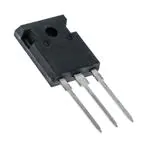
TO-268 (IXFT)
G
S
D (Tab)
Symbol
Test Conditions
Maximum Ratings
VDSS
TJ = 25°C to 150°C
1200
V
VDGR
TJ = 25°C to 150°C, RGS = 1MΩ
1200
V
VGSS
VGSM
Continuous
Transient
± 30
± 40
V
V
ID25
TC = 25°C
16
A
IDM
TC = 25°C, Pulse Width Limited by TJM
35
A
IA
TC = 25°C
8
A
EAS
TC = 25°C
800
mJ
dv/dt
IS ≤ IDM, VDD ≤ VDSS, TJ ≤ 150°C
15
V/ns
PD
TC = 25°C
660
W
-55 ... +150
°C
TJM
150
°C
Tstg
-55 ... +150
°C
300
260
°C
°C
1.13 / 10
Nm/lb.in.
4
6
g
g
TJ
TL
Tsold
1.6mm (0.062in.) from Case for 10s
Plastic Body for 10 seconds
Md
Mounting Torque (TO-247)
Weight
TO-268
TO-247
TO-247 (IXFH)
G
BVDSS
VGS = 0V, ID = 1mA
1200
VGS(th)
VDS = VGS, ID = 1mA
3.5
IGSS
VGS = ±30V, VDS = 0V
IDSS
VDS = VDSS, VGS= 0V
RDS(on)
TJ = 125°C
VGS = 10V, ID = 0.5 • ID25, Note 1
© 2012 IXYS CORPORATION, All Rights Reserved
D (Tab)
D
= Drain
Tab = Drain
Features
z
z
z
z
International Standard Packages
Fast Recovery Diode
Avalanche Rated
Low Package Inductance
Advantages
z
z
Characteristic Values
Min.
Typ.
Max.
S
G = Gate
S = Source
z
Symbol
Test Conditions
(TJ = 25°C Unless Otherwise Specified)
D
Easy to Mount
Space Savings
High Power Density
Applications
z
V
6.5
V
±200
nA
25 μA
2.5 mA
z
z
z
z
High Voltage Switch-mode and
Resonant-Mode Power Supplies
High Voltage Pulse Power Applications
High Voltage Discharge Circuits in
Lasers Pulsers, Spark Igniters, RF
Generators
High Voltage DC-DC converters
High Voltage DC-AC inverters
950 mΩ
DS99896B(10/12)
�IXFT16N120P
IXFH16N120P
Symbol
Test Conditions
(TJ = 25°C Unless Otherwise Specified)
gfs
Characteristic Values
Min.
Typ.
Max.
VDS = 20V, ID = 0.5 • ID25, Note 1
11
Ciss
17
S
6900
pF
390
pF
48
pF
1.4
Ω
35
ns
VGS = 0V, VDS = 25V, f = 1MHz
Coss
Crss
RGi
Gate Input Resistance
td(on)
Resistive Switching Times
tr
TO-268 Outline
28
ns
td(off)
VGS = 10V, VDS = 0.5 • VDSS, ID = 0.5 • ID25
66
ns
tf
RG = 2Ω (External)
35
ns
120
nC
37
nC
47
nC
Qg(on)
VGS = 10V, VDS = 0.5 • VDSS, ID = 0.5 • ID25
Qgs
Qgd
Terminals: 1 - Gate
3 - Source
2,4 - Drain
0.19 °C/W
RthJC
RthCS
TO-247
°C/W
0.21
Source-Drain Diode
Symbol
Test Conditions
(TJ = 25°C Unless Otherwise Specified)
Characteristic Values
Min.
Typ.
Max.
IS
VGS = 0V
16
A
ISM
Repetitive, Pulse Width Limited by TJM
64
A
VSD
IF = IS, VGS = 0V, Note 1
1.5
V
300
ns
trr
IF = 8A, -di/dt = 100A/μs
IRM
VR = 100V, VGS = 0V
QRM
7.5
A
0.75
μC
TO-247 Outline
1
2
∅P
3
e
Terminals: 1 - Gate
3 - Source
Note
1.
Pulse test, t ≤ 300μs, duty cycle, d ≤ 2%.
Dim.
Millimeter
Min. Max.
A
4.7
5.3
2.2
2.54
A1
A2
2.2
2.6
b
1.0
1.4
1.65
2.13
b1
b2
2.87
3.12
C
.4
.8
D
20.80 21.46
E
15.75 16.26
e
5.20
5.72
L
19.81 20.32
L1
4.50
∅P 3.55
3.65
Q
5.89
6.40
R
4.32
5.49
S
6.15 BSC
2 - Drain
Inches
Min. Max.
.185 .209
.087 .102
.059 .098
.040 .055
.065 .084
.113 .123
.016 .031
.819 .845
.610 .640
0.205 0.225
.780 .800
.177
.140 .144
0.232 0.252
.170 .216
242 BSC
IXYS Reserves the Right to Change Limits, Test Conditions, and Dimensions.
IXYS MOSFETs and IGBTs are covered
4,835,592
by one or moreof the following U.S. patents: 4,860,072
4,881,106
4,931,844
5,017,508
5,034,796
5,049,961
5,063,307
5,187,117
5,237,481
5,381,025
5,486,715
6,162,665
6,259,123 B1
6,306,728 B1
6,404,065 B1
6,534,343
6,583,505
6,683,344
6,727,585
7,005,734 B2
6,710,405 B2 6,759,692
7,063,975 B2
6,710,463
6,771,478 B2 7,071,537
7,157,338B2
�IXFT16N120P
IXFH16N120P
Fig. 1. Output Characteristics T J = @ 25ºC
Fig. 2. Extended Output Characteristics T J = @ 25ºC
16
20
12
7V
10
ID - Amperes
ID - Amperes
VGS = 10V
8V
24
VGS = 10V
8V
14
8
6
6V
7V
16
12
6V
8
4
4
2
5V
5V
0
0
0
2
4
6
8
10
12
14
16
0
5
10
15
25
30
Fig. 4. RDS(on) Normalized to ID = 8A Value vs.
Junction Temperature
Fig. 3. Output Characteristics T J = @ 125ºC
16
2.8
VGS = 10V
8V
7V
14
VGS = 10V
2.4
R DS(on) - Normalized
12
ID - Amperes
20
VDS - Volts
VDS - Volts
10
6V
8
6
I D = 16A
2.0
I D = 8A
1.6
1.2
4
0.8
2
5V
0
0.4
0
5
10
15
20
25
30
35
-50
-25
0
VDS - Volts
Fig. 5. RDS(on) Normalized to ID = 8A Value vs.
Drain Current
50
75
100
125
150
125
150
Fig. 6. Maximum Drain Current vs.
Case Temperature
2.4
18
16
VGS = 10V
2.2
TJ = 125ºC
14
2.0
12
1.8
ID - Amperes
R DS(on) - Normalized
25
TJ - Degrees Centigrade
1.6
1.4
10
8
6
1.2
4
TJ = 25ºC
1.0
2
0
0.8
0
2
4
6
8
10
12
14
16
ID - Amperes
© 2012 IXYS CORPORATION, All Rights Reserved
18
20
22
24
26
-50
-25
0
25
50
75
TC - Degrees Centigrade
100
�IXFT16N120P
IXFH16N120P
Fig. 7. Input Admittance
18
14
16
g f s - Siemens
10
TJ = - 40ºC
14
TJ = 125ºC
25ºC
- 40ºC
12
ID - Amperes
Fig. 8. Transconductance
16
8
6
4
12
25ºC
10
125ºC
8
6
4
2
2
0
0
3.5
4.0
4.5
5.0
5.5
6.0
6.5
7.0
0
2
4
6
VGS - Volts
Fig. 9. Forward Voltage Drop of Intrinsic Diode
10
12
14
16
Fig. 10. Gate Charge
50
10
45
9
40
8
35
7
VGS - Volts
IS - Amperes
8
ID - Amperes
30
25
20
VDS = 600V
I D = 8A
I G = 10mA
6
5
4
TJ = 125ºC
3
15
TJ = 25ºC
10
2
1
5
0
0
0.3
0.4
0.5
0.6
0.7
0.8
0.9
1.0
1.1
1.2
0
1.3
20
40
VSD - Volts
60
80
100
120
QG - NanoCoulombs
Fig. 12. Breakdown and Threshold Voltages vs.
Junction Temperature
Fig. 11. Capacitance
1.2
100,000
BVDSS & VGS(th) - Normalized
Capacitance - PicoFarads
f = 1 MHz
Ciss
10,000
1,000
Coss
100
1.1
BVDSS
1
0.9
VGS(th)
0.8
Crss
10
0.7
0
5
10
15
20
25
30
35
40
VDS - Volts
IXYS Reserves the Right to Change Limits, Test Conditions, and Dimensions.
-50
-25
0
25
50
75
TJ - Degrees Centigrade
100
125
150
�IXFT16N120P
IXFH16N120P
Fig. 12. Maximum Transient Thermal Impedance
1.00
Fig. 13. Maximum Transient Thermal Impedance
aaa
0.30
Z(th)JC - ºC / W
0.10
0.01
0.0001
0.001
0.01
0.1
1
10
Pulse Width - Seconds
© 2012 IXYS CORPORATION, All Rights Reserved
IXYS REF: F_16N120P(85) 09-12-12-B
�Disclaimer Notice - Information furnished is believed to be accurate and reliable. However, users should independently
evaluate the suitability of and test each product selected for their own applications. Littelfuse products are not designed for,
and may not be used in, all applications. Read complete Disclaimer Notice at www.littelfuse.com/disclaimer-electronics.
�


 工商网监
湘ICP备2023018690号
工商网监
湘ICP备2023018690号
