Preliminary Technical Information
IXTL2x180N10T
TrenchTM Power MOSFET
Common-Gate Pair
VDSS
ID25
=
=
RDS(on) ≤
100V
2x100A
Ω
9mΩ
(Electrically Isolated Back Surface)
N-Channel Enhancement Mode
Avalanche Rated
Fast Intrinsic Rectifier
Symbol
Test Conditions
Maximum Ratings
VDSS
VDGR
TJ = 25°C to 175°C
TJ = 25°C to 175°C, RGS = 1MΩ
100
100
V
V
VGSS
VGSM
Continuous
Transient
± 20
± 30
V
V
ID25
IL(RMS)
IDM
TC = 25°C
External Lead Current Limit
TC = 25°C, Pulse Width Limited by TJM
100
75
450
A
A
A
IA
EAS
TC = 25°C
TC = 25°C
25
750
A
mJ
PD
TC = 25°C
150
W
dv/dt
IS ≤ IDM, VDD ≤ VDSS, TJ ≤ 175°C
3
V/ns
-55 ... +175
175
-55 ... +175
°C
°C
°C
300
260
°C
°C
TJ
TJM
Tstg
TL
TSOLD
1.6mm (0.062 in.) from Case for 10s
Plastic Body for 10s
FC
Mounting Force
20..120 /9..27
N/lb.
8
g
Weight
Features
Silicon Chip on Direct-Copper Bond
(DCB) Substrate
z
Isolated Mounting Surface
z
2500V~ Electrical Isolation
z
175°C Operating Temperature
z
Avalanche Rated
z
High Current Handling Capability
z
Fast Intrinsic Rectifier
z
Low RDS(on) and QG
z
Advantages
z
z
z
High Power Density
Easy to Mount
Space Savings
Applications
z
Symbol
Test Conditions
(TJ = 25°C Unless Otherwise Specified)
Characteristic Values
Min.
Typ.
Max.
BVDSS
VGS = 0V, ID = 250μA
100
VGS(th)
VDS = VGS, ID = 250μA
2.5
IGSS
VGS = ± 20V, VDS = 0V
IDSS
VDS = VDSS, VGS = 0V
RDS(on)
VGS = 10V, ID = 50A, Note 1
TJ = 150°C
© 2012 IXYS CORPORATION, All Rights Reserved
V
4.5
V
± 200
nA
5
250
μA
μA
z
z
z
z
z
9 mΩ
z
Automotive
- Motor Drives
- DC/DC Conversion
- 42V Power Bus
- ABS Systems
DC/DC Converters and Off-Line UPS
Primary Switch for 24V and 48V
Systems
High Current Switching Applications
Distributed Power Architechtures
and VRMs
Electronic Valve Train Systems
High Voltage Synchronous Recifier
DS99752B(05/12)
�IXTL2x180N10T
Symbol
Test Conditions
(TJ = 25°C, Unless Otherwise Specified)
Characteristic Values
Min.
Typ.
Max.
gfs
70
VDS = 10V, ID = 60A, Note 1
Ciss
110
S
6900
pF
923
pF
162
pF
3.0
Ω
33
ns
54
ns
42
ns
31
ns
151
nC
39
nC
45
nC
VGS = 0V, VDS = 25V, f = 1MHz
Coss
Crss
RGi
Gate Input Resistance
td(on)
Resistive Switching Times
tr
VGS = 10V, VDS = 0.5 • VDSS, ID = 25A
td(off)
RG = 3.3Ω (External)
tf
Qg(on)
VGS = 10V, VDS = 0.5 • VDSS, ID = 25A
Qgs
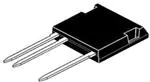
ISOPLUS I5-PakTM (IXTL) Outline
Qgd
1,5 = Drain
2,4 = Source
3 = Gate
6 = Isolated
1.0 °C/W
RthJC
RthCS
0.15
°C/W
Source-Drain Diode
Symbol
Test Conditions
(TJ = 25°C, Unless Otherwise Specified)
Characteristic Values
Min.
Typ.
Max.
IS
VGS = 0V
180
A
ISM
Repetitive, Pulse Width Limited by TJM
450
A
VSD
IF = 50A, VGS = 0V, Note 1
1.0
V
trr
60
IF = 25A, VGS = 0V
ns
-di/dt = 100A/μs, VR = 50V
Note
1.
Pulse test, t ≤ 300μs, duty cycle, d ≤ 2%.
PRELIMINARY TECHNICAL INFORMATION
The product presented herein is under development. The Technical Specifications offered are derived
from data gathered during objective characterizations of preliminary engineering lots; but also may yet
contain some information supplied during a pre-production design evaluation. IXYS reserves the right
to change limits, test conditions, and dimensions without notice.
IXYS Reserves the Right to Change Limits, Test Conditions, and Dimensions.
IXYS MOSFETs and IGBTs are covered
4,835,592
by one or more of the following U.S. patents: 4,860,072
4,881,106
4,931,844
5,017,508
5,034,796
5,049,961
5,063,307
5,187,117
5,237,481
5,381,025
5,486,715
6,162,665
6,259,123 B1
6,306,728 B1
6,404,065 B1
6,534,343
6,583,505
6,683,344
6,727,585
7,005,734 B2
6,710,405 B2 6,759,692
7,063,975 B2
6,710,463
6,771,478 B2 7,071,537
7,157,338B2
�Disclaimer Notice - Information furnished is believed to be accurate and reliable. However, users should independently
evaluate the suitability of and test each product selected for their own applications. Littelfuse products are not designed for,
and may not be used in, all applications. Read complete Disclaimer Notice at www.littelfuse.com/disclaimer-electronics.
�


 工商网监
湘ICP备2023018690号
工商网监
湘ICP备2023018690号
