Advance Technical Information
IXTT1N250HV
High Voltage
Power MOSFET
VDSS
ID25
RDS(on)
= 2500V
= 1.5A
Ω
≤ 40Ω
N-Channel Enhancement Mode
Fast Intrinsic Diode
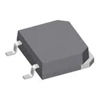
TO-268S
G
S
D (Tab)
Symbol
Test Conditions
Maximum Ratings
VDSS
TJ = 25°C to 150°C
2500
V
VDGR
TJ = 25°C to 150°C, RGS = 1MΩ
2500
V
VGSS
Continuous
±20
V
VGSM
Transient
±30
V
ID25
TC = 25°C
1.5
A
IDM
TC = 25°C, Pulse Width Limited by TJM
6
A
PD
TC = 25°C
250
W
- 55 ... +150
150
- 55 ... +150
°C
°C
°C
300
260
°C
°C
4
g
TJ
TJM
Tstg
TL
TSOLD
1.6mm (0.062 in.) From Case for 10s
Plastic Body for 10s
Weight
G = Gate
S = Source
D
= Drain
Tab = Drain
Features
z
z
z
z
High Blocking Voltage
High Voltage Package
Fast Intrinsic Diode
Low Package Inductance
Advantages
z
z
z
Symbol
Test Conditions
(TJ = 25°C, Unless Otherwise Specified)
Characteristic Values
Min.
Typ.
Max.
BVDSS
VGS = 0V, ID = 250μA
2500
VGS(th)
VDS = VGS, ID = 250μA
2.0
IGSS
VGS = ±20V, VDS = 0V
IDSS
VDS = 0.8 • VDSS, VGS = 0V
RDS(on)
VGS = 10V, ID = 0.5 • ID25, Note 1
Applications
V
4.0
V
±100 nA
TJ = 125°C
© 2012 IXYS CORPORATION, All Rights Reserved
25
Easy to Mount
Space Savings
High Power Density
z
z
z
High Voltage Power Supplies
Capacitor Discharge
Pulse Circuits
25 μA
μA
40
Ω
DS100521(12/12)
�IXTT1N250HV
Symbol
Test Conditions
(TJ = 25°C, Unless Otherwise Specified)
gfs
Characteristic Values
Min.
Typ.
Max.
VDS = 50V, ID = 0.5A, Note 1
1.0
Ciss
TO-268 (VHV) Outline
1.8
mS
1660
pF
77
pF
Crss
23
pF
td(on)
69
ns
25
ns
132
ns
39
ns
41
nC
Coss
tr
td(off)
tf
VGS = 0V, VDS = 25V, f = 1MHz
Resistive Switching Times
VGS = 10V, VDS = 0.5 • VDSS, ID = 1A
RG = 5Ω (External)
Qg(on)
Qgs
VGS = 10V, VDS = 600V, ID = 0.5A
Qgd
8
nC
16
nC
PIN:
1 - Gate
2 - Source
3 - Drain
0.50 °C/W
RthJC
RthCS
°C/W
0.21
Source-Drain Diode
Symbol
Test Conditions
(TJ = 25°C, Unless Otherwise Specified)
Characteristic Values
Min.
Typ.
Max.
IS
VGS = 0V
ISM
Repetitive, Pulse Width Limited by TJM
VSD
IF = 1A, VGS = 0V, Note 1
trr
IF = 1A, -di/dt = 100A/μs, VR = 200V
Note
2.5
1.5
A
6
A
1.5
V
μs
1. Pulse test, t ≤ 300μs, duty cycle, d ≤ 2%.
ADVANCE TECHNICAL INFORMATION
The product presented herein is under development. The Technical Specifications offered are derived
from a subjective evaluation of the design, based upon prior knowledge and experience, and constitute a
"considered reflection" of the anticipated result. IXYS reserves the right to change limits, test
conditions, and dimensions without notice.
IXYS Reserves the Right to Change Limits, Test Conditions, and Dimensions.
IXYS MOSFETs and IGBTs are covered
4,835,592
by one or moreof the following U.S. patents: 4,860,072
4,881,106
4,931,844
5,017,508
5,034,796
5,049,961
5,063,307
5,187,117
5,237,481
5,381,025
5,486,715
6,162,665
6,259,123 B1
6,306,728 B1
6,404,065 B1
6,534,343
6,583,505
6,683,344
6,727,585
7,005,734 B2
6,710,405 B2 6,759,692
7,063,975 B2
6,710,463
6,771,478 B2 7,071,537
7,157,338B2
�IXTT1N250HV
Fig. 2. Output Characteristics @ T J = 125ºC
Fig. 1. Output Characteristics @ T J = @ 25ºC
1
1
VGS = 10V
0.8
0.8
5V
0.7
5V
0.7
ID - Amperes
ID - Amperes
VGS = 10V
0.9
0.9
0.6
0.5
0.4
0.6
0.5
4V
0.4
0.3
0.3
0.2
0.2
4V
0.1
0.1
0
0
0
5
10
15
20
25
30
35
40
45
0
10
20
30
40
50
60
70
80
90
VDS - Volts
VDS - Volts
Fig. 4. RDS(on) Normalized to ID = 0.5A Value vs.
Junction Temperature
Fig. 3. RDS(on) Normalized to ID = 0.5A Value vs.
Drain Current
2.4
2.6
VGS = 10V
VGS = 10V
2.2
R DS(on) - Normalized
R DS(on) - Normalized
2.2
1.8
I D = 1A
1.4
I D = 0.5A
1.0
TJ = 125ºC
2.0
1.8
1.6
1.4
1.2
0.6
TJ = 25ºC
1.0
0.8
0.2
-50
-25
0
25
50
75
100
125
0
150
0.1
0.2
0.3
TJ - Degrees Centigrade
Fig. 5. Maximum Drain Current vs.
Case Temperature
0.5
0.6
0.7
0.8
0.9
1
Fig. 6. Input Admittance
1.6
0.9
1.4
0.8
0.7
ID - Amperes
1.2
ID - Amperes
0.4
ID - Amperes
1
0.8
0.6
0.6
0.5
0.4
TJ = 125ºC
25ºC
- 40ºC
0.3
0.4
0.2
0.2
0.1
0
0
-50
-25
0
25
50
75
TC - Degrees Centigrade
© 2012 IXYS CORPORATION, All Rights Reserved
100
125
150
2.8
3.0
3.2
3.4
3.6
3.8
4.0
VGS - Volts
4.2
4.4
4.6
4.8
5.0
�IXTT1N250HV
Fig. 8. Forward Voltage Drop of
Intrinsic Diode
Fig. 7. Transconductance
3
3
TJ = - 40ºC
2.5
2.5
2
2
IS - Amperes
g f s - Siemens
25ºC
125ºC
1.5
1.5
TJ = 125ºC
1
1
0.5
0.5
0
TJ = 25ºC
0
0
0.1
0.2
0.3
0.4
0.5
0.6
0.7
0.8
0.9
1
0.3
0.4
0.5
ID - Amperes
Fig. 9. Gate Charge
0.7
0.8
0.9
Fig. 10. Capacitance
10
10,000
f = 1MHz
VDS = 600V
9
I D = 500mA
8
Capacitance - PicoFarads
I G = 10mA
7
VGS - Volts
0.6
VSD - Volts
6
5
4
3
Ciss
1,000
Coss
100
2
1
Crss
0
10
0
5
10
15
20
25
30
35
40
45
0
5
10
15
20
25
30
35
40
VDS - Volts
QG - NanoCoulombs
Fig. 11. Forward-Bias Safe Operating Area
Fig. 12. Forward-Bias Safe Operating Area
@ T C = 25ºC
@ T C = 75ºC
10
10
RDS(on) Limit
RDS(on) Limit
25µs
25µs
100µs
1
ID - Amperes
ID - Amperes
100µs
1
1ms
10ms
100ms
0.1
1ms
10ms
0.1
100ms
DC
0.01
100
TJ = 150ºC
TJ = 150ºC
TC = 25ºC
Single Pulse
TC = 75ºC
Single Pulse
1,000
10,000
VDS - Volts
IXYS Reserves the Right to Change Limits, Test Conditions, and Dimensions.
0.01
100
DC
1,000
VDS - Volts
10,000
�IXTT1N250HV
Fig. 13. Maximum Transient Thermal Impedance
Z (th )J C - ºC / W
1
0.1
0.01
0.0001
0.001
0.01
0.1
1
10
Pulse Width - Seconds
© 2012 IXYS CORPORATION, All Rights Reserved
IXYS REF: T_1N250 (5P)10-25-10-D
�Disclaimer Notice - Information furnished is believed to be accurate and reliable. However, users should independently
evaluate the suitability of and test each product selected for their own applications. Littelfuse products are not designed for,
and may not be used in, all applications. Read complete Disclaimer Notice at www.littelfuse.com/disclaimer-electronics.
�


 工商网监
湘ICP备2023018690号
工商网监
湘ICP备2023018690号
