CM1213A, SZCM1213A
1, 2 and 4-Channel
Low Capacitance
ESD Protection Arrays
Product Description
The CM1213A family of diode arrays has been designed to provide
ESD protection for electronic components or subsystems requiring
minimal capacitive loading. These devices are ideal for protecting
systems with high data and clock rates or for circuits requiring low
capacitive loading. Each ESD channel consists of a pair of diodes in
series which steer the positive or negative ESD current pulse to either
the positive (VP) or negative (VN) supply rail. A Zener diode is
embedded between VP and VN, offering two advantages. First, it
protects the VCC rail against ESD strikes, and second, it eliminates the
need for a bypass capacitor that would otherwise be needed for
absorbing positive ESD strikes to ground. The CM1213A will protect
against ESD pulses up to 12 kV per the IEC 61000−4−2 standard.
www.onsemi.com
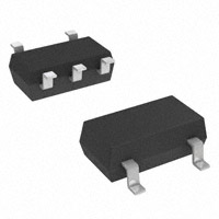
SOT23−3
SO SUFFIX
CASE 318
• One, Two, and Four Channels of ESD Protection
Note: For 6 and 8−channel Devices, See the CM1213 Datasheet
MARKING DIAGRAMS
• Provides ESD Protection to IEC61000−4−2 Level 4
±12 kV Contact Discharge
• Low Channel Input Capacitance of 0.85 pF Typical
• Minimal Capacitance Change with Temperature and Voltage
• Channel Input Capacitance Matching of 0.02 pF Typical is Ideal for
•
•
•
SC−74
SO SUFFIX
CASE 318F
MSOP−10
MR SUFFIX
CASE 846AE
SC70−6
S7 SUFFIX
CASE 419AD
Features
♦
SOT−143
SR SUFFIX
CASE 318A
Differential Dignals
Each I/O Pin Can Withstand Over 1000 ESD Strikes*
SZ Prefix for Automotive and Other Applications Requiring Unique
Site and Control Change Requirements; AEC−Q101 Qualified and
PPAP Capable
These Devices are Pb−Free, Halogen Free/BFR Free and are RoHS
Compliant
XXXMG
G
XXXMG
G
1
1
XXX
M
G
= Specific Device Code
= Date Code
= Pb−Free Package
10
XXXX
AYWG
G
1
Applications
• USB2.0 Ports at 480 Mbps in Desktop PCs, Notebooks and Peripherals
• IEEE1394 Firewire® Ports at 400 Mbps/800 Mbps
• DVI Ports, HDMI Ports in Notebooks, Set Top Boxes, Digital TVs,
LCD Displays
• Serial ATA Ports in Desktop PCs and Hard Disk Drives
• PCI Express Ports
• General Purpose High−Speed Data Line ESD Protection
XXXX
A
Y
W
G
= Specific Device Code
= Assembly Location
= Year
= Work Week
= Pb−Free Package
(Note: Microdot may be in either location)
ORDERING INFORMATION
See detailed ordering, marking and shipping information in the
package dimensions section on page 2 of this data sheet.
*Standard test condition is IEC61000−4−2 level 4 test circuit with each pin subjected to ±8 kV contact discharge for 1000 pulses. Discharges
are timed at 1 second intervals and all 1000 strikes are completed in one continuous test run. The part is then subjected to standard production
test to verify that all of the tested parameters are within spec after the 1000 strikes.
© Semiconductor Components Industries, LLC, 2011
June, 2018 − Rev. 14
1
Publication Order Number:
CM1213A/D
�CM1213A, SZCM1213A
BLOCK DIAGRAM
VP
CH1
VN
CM1213A−01SO
VP
CH4
CH1
VP
CH3
CH2
VN
CM1213A−02SR
CM1213A−02SO
CH1 VN CH2
CM1213A−04MR
CM1213A−04S7
Table 1. ORDERING INFORMATION
Marking
Package
Shipping†
231
SOT23−3
(Pb−Free)
3,000 / Tape & Reel
D232
SOT143−4
(Pb−Free)
3,000 / Tape & Reel
CM1213A−02SO
233
SC−74
(Pb−Free)
3,000 / Tape & Reel
CM1213A−04S7
D38
SC70−6
(Pb−Free)
3,000 / Tape & Reel
CM1213A−04MR
D237
MSOP−10
(Pb−Free)
4,000 / Tape & Reel
Device
CM1213A−01SO
SZCM1213A−01SO*
CM1213A−02SR
SZCM1213A−02SR*
†For information on tape and reel specifications, including part orientation and tape sizes, please refer to our Tape and Reel Packaging
Specifications Brochure, BRD8011/D.
*SZ Prefix for Automotive and Other Applications Requiring Unique Site and Control Change Requirements; AEC−Q101 Qualified and PPAP
Capable.
www.onsemi.com
2
�CM1213A, SZCM1213A
PACKAGE/PINOUT DIAGRAMS
Table 2. PIN DESCRIPTIONS
1−Channel, 3−Lead SOT23−3 Package (CM1213A−01SO)
Top View
Pin
Name
Type
Description
1
CH1
I/O
2
VP
PWR
Positive Voltage Supply Rail
3
VN
GND
Negative Voltage Supply Rail
CH1 (1)
ESD Channel
1
231
VP (2)
3
VN (3)
2
3−Lead SOT23−3
2−Channel, 4−Lead SOT143−4 Package (CM1213A−02SR)
Pin
Name
Type
1
VN
GND
Description
2
CH1
I/O
ESD Channel
3
CH2
I/O
ESD Channel
4
VP
PWR
Negative Voltage Supply Rail
Top View
1
CH1 (2)
2
4
VP (4)
3
CH2 (3)
D232
VN (1)
Positive Voltage Supply Rail
2−Channel, SC−74 Package (CM1213A−02SO)
Pin
Name
Type
1
NC
−
2
VN
GND
3
CH1
I/O
ESD Channel
4
CH2
I/O
ESD Channel
5
NC
−
6
VP
PWR
4−Lead SOT143−4
Description
No Connect
Negative Voltage Supply Rail
Top View
NC (1)
1
VN (2)
2
CH1 (3)
3
233
No Connect
6
VP (6)
5
NC (5)
4
CH2 (4)
Positive Voltage Supply Rail
6−Lead SC−74
4−Channel, 6−Lead SC70−6 (CM1213A−04S7)
Pin
Name
Type
1
CH1
I/O
Description
2
VN
GND
3
CH2
I/O
ESD Channel
4
CH3
I/O
ESD Channel
5
VP
PWR
6
CH4
I/O
ESD Channel
Negative Voltage Supply Rail
Top View
ESD Channel
1
VN
2
CH2
3
D38
Positive Voltage Supply Rail
CH1
6
CH4
5
VP
4
CH3
6−Lead SC70−6
4−Channel, 10−Lead MSOP−10 Package (CM1213A04MR)
Pin
Name
Type
1
CH1
I/O
2
NC
−
3
VP
PWR
CH2
I/O
NC
−
6
CH3
I/O
7
NC
−
8
VN
GND
9
CH4
I/O
10
NC
−
ESD Channel
No Connect
Top View
Positive Voltage Supply Rail
CH1
NC
VP
CH2
NC
ESD Channel
No Connect
ESD Channel
1
2
3
4
5
D238
4
5
Description
10
9
8
7
6
NC
CH4
VN
NC
CH3
10−Lead MSOP−10
No Connect
Negative Voltage Supply Rail
ESD Channel
No Connect
www.onsemi.com
3
�CM1213A, SZCM1213A
SPECIFICATIONS
Table 3. ABSOLUTE MAXIMUM RATINGS
Parameter
Rating
Units
6.0
V
Operating Temperature Range
–40 to +150
°C
Storage Temperature Range
–65 to +150
°C
Operating Supply Voltage (VP − VN)
DC Voltage at any channel input
(VN − 0.5) to (VP + 0.5)
Package Power Rating
SOT23−3, SOT143−4, SC−74, and SC70−6 Packages
MSOP−10 Package
225
400
ESD
IEC 61000−4−2 Contact
IEC 61000−4−2 Air
ISO 10605 330 pF / 330 W Contact
ISO 10605 330 pF / 2 kW Contact
ISO 10605 150 pF / 2 kW Contact
±12
±12
±9
±22
±25
V
mW
kV
Stresses exceeding those listed in the Maximum Ratings table may damage the device. If any of these limits are exceeded, device functionality
should not be assumed, damage may occur and reliability may be affected.
Table 4. ELECTRICAL OPERATING CHARACTERISTICS (Note1)
Symbol
Parameter
Conditions
VP
Operating Supply Voltage (VP−VN)
IP
Operating Supply Current
(VP−VN) = 3.3 V
VF
Diode Forward Voltage
Top Diode
Bottom Diode
IF = 8 mA; TA = 25°C
Channel Leakage Current
Channel Input Capacitance
ILEAK
CIN
DCIN
VCL
RDYN
Min
Typ
Max
Units
3.3
5.5
V
8.0
mA
V
0.60
0.60
0.80
0.80
0.95
0.95
TA = 25°C; VP = 5 V, VN = 0 V
0.1
1.0
mA
At 1 MHz, VP = 3.3 V, VN = 0 V, VIN = 1.65 V
(Note 2)
0.85
1.2
pF
Channel Input Capacitance Matching
At 1 MHz, VP = 3.3 V, VN = 0 V, VIN = 1.65 V
(Note 2)
0.02
Channel Clamp Voltage
Positive Transients
Negative Transients
TA = 25°C, IPP = 1A, tP = 8/20 mS
(Note 2)
Dynamic Resistance
Positive Transients
Negative Transients
IPP = 1A, tP = 8/20 mS
Any I/O pin to Ground
(Note 2)
pF
V
+10
–1.7
W
0.9
0.5
Product parametric performance is indicated in the Electrical Characteristics for the listed test conditions, unless otherwise noted. Product
performance may not be indicated by the Electrical Characteristics if operated under different conditions.
1. All parameters specified at TA = 25°C unless otherwise noted.
2. Standard IEC 61000−4−2 with CDischarge = 150 pF, RDischarge = 330 W, VP = 3.3 V, VN grounded.
3. These measurements performed with no external capacitor on VP (VP floating).
www.onsemi.com
4
�CM1213A, SZCM1213A
PERFORMANCE INFORMATION
Input Channel Capacitance Performance Curves
Figure 1. Typical Variation of CIN vs. VIN
(f = 1 MHz, VP = 3.3 V, VN = 0 V, 0.1 �F Chip Capacitor between VP and VN, 255C)
Figure 2. Typical Variation of CIN vs. Temp
(f = 1 MHz, VIN = 30 mV, VP = 3.3 V, VN = 0 V, 0.1 �F Chip Capacitor between VP and VN)
www.onsemi.com
5
�CM1213A, SZCM1213A
PERFORMANCE INFORMATION (Cont’d)
Typical Filter Performance (nominal conditions unless specified otherwise, 50 Ohm Environment)
Figure 3. Insertion Loss (S21) vs. Frequency (0 V DC Bias, VP=3.3 V)
Figure 4. Insertion Loss (S21) vs. Frequency (2.5 V DC Bias, VP=3.3 V)
www.onsemi.com
6
�CM1213A, SZCM1213A
APPLICATION INFORMATION
Design Considerations
In order to realize the maximum protection against ESD pulses, care must be taken in the PCB layout to minimize parasitic
series inductances on the Supply/Ground rails as well as the signal trace segment between the signal input (typically
a connector) and the ESD protection device. Refer to Application of Positive ESD Pulse between Input Channel and Ground,
which illustrates an example of a positive ESD pulse striking an input channel. The parasitic series inductance back to the power
supply is represented by L1 and L2. The voltage VCL on the line being protected is:
VCL = Fwd Voltage Drop of D1 + VSUPPLY + L1 x d(IESD) / dt + L2 x d(IESD) / dt
where IESD is the ESD current pulse, and VSUPPLY is the positive supply voltage.
An ESD current pulse can rise from zero to its peak value in a very short time. As an example, a level 4 contact discharge
per the IEC61000−4−2 standard results in a current pulse that rises from zero to 30 Amps in 1 ns. Here d(IESD)/dt can be
approximated by DIESD/Dt, or 30/(1x10−9). So just 10 nH of series inductance (L1 and L2 combined) will lead to a 300 V
increment in VCL!
Similarly for negative ESD pulses, parasitic series inductance from the VN pin to the ground rail will lead to drastically
increased negative voltage on the line being protected.
The CM1213A has an integrated Zener diode between VP and VN. This greatly reduces the effect of supply rail inductance
L2 on VCL by clamping VP at the breakdown voltage of the Zener diode. However, for the lowest possible VCL, especially when
VP is biased at a voltage significantly below the Zener breakdown voltage, it is recommended that a 0.22 mF ceramic chip
capacitor be connected between VP and the ground plane.
As a general rule, the ESD Protection Array should be located as close as possible to the point of entry of expected
electrostatic discharges. The power supply bypass capacitor mentioned above should be as close to the VP pin of the Protection
Array as possible, with minimum PCB trace lengths to the power supply, ground planes and between the signal input and the
ESD device to minimize stray series inductance.
Additional Information
See also ON Semiconductor Application Note “Design Considerations for ESD Protection”, in the Applications section.
L2
POSITIVE SUPPLY RAIL
VP
ÇÇÇÇÇÇ
ÇÇÇÇÇÇ
ÇÇÇÇÇÇ
ÇÇÇÇÇÇ
ÇÇÇÇÇÇ
ÇÇÇÇÇÇ
D1
0.22 mF
ONE
CHANNEL
D2 OF
CM1213
VN
VCC
PATH OF ESD CURRENT PULSE IESO
LINE BEING
PROTECTED
L1
0A
SYSTEM OR
CIRCUITRY
BEING
PROTECTED
CHANNEL
INPUT
25 A
ÇÇÇÇÇÇ
ÇÇÇÇÇÇ
ÇÇÇÇÇÇ
ÇÇÇÇÇÇ
ÇÇÇÇÇÇ
VCL
GROUND RAIL
CHASSIS GROUND
Figure 5. Application of Positive ESD Pulse between Input Channel and Ground
www.onsemi.com
7
�MECHANICAL CASE OUTLINE
PACKAGE DIMENSIONS
SOT−23 (TO−236)
CASE 318−08
ISSUE AS
DATE 30 JAN 2018
SCALE 4:1
D
0.25
3
E
1
2
T
HE
NOTES:
1. DIMENSIONING AND TOLERANCING PER ASME Y14.5M, 1994.
2. CONTROLLING DIMENSION: MILLIMETERS.
3. MAXIMUM LEAD THICKNESS INCLUDES LEAD FINISH.
MINIMUM LEAD THICKNESS IS THE MINIMUM THICKNESS OF
THE BASE MATERIAL.
4. DIMENSIONS D AND E DO NOT INCLUDE MOLD FLASH,
PROTRUSIONS, OR GATE BURRS.
DIM
A
A1
b
c
D
E
e
L
L1
HE
T
L
3X b
L1
VIEW C
e
TOP VIEW
A
A1
SIDE VIEW
MIN
0.89
0.01
0.37
0.08
2.80
1.20
1.78
0.30
0.35
2.10
0°
MILLIMETERS
NOM
MAX
1.00
1.11
0.06
0.10
0.44
0.50
0.14
0.20
2.90
3.04
1.30
1.40
1.90
2.04
0.43
0.55
0.54
0.69
2.40
2.64
−−−
10 °
MIN
0.035
0.000
0.015
0.003
0.110
0.047
0.070
0.012
0.014
0.083
0°
INCHES
NOM
0.039
0.002
0.017
0.006
0.114
0.051
0.075
0.017
0.021
0.094
−−−
MAX
0.044
0.004
0.020
0.008
0.120
0.055
0.080
0.022
0.027
0.104
10°
c
SEE VIEW C
GENERIC
MARKING DIAGRAM*
END VIEW
RECOMMENDED
SOLDERING FOOTPRINT
XXXMG
G
1
3X
2.90
3X
XXX = Specific Device Code
M = Date Code
G
= Pb−Free Package
(Note: Microdot may be in either location)
0.90
*This information is generic. Please refer to
device data sheet for actual part marking.
Pb−Free indicator, “G” or microdot “ G”,
may or may not be present.
0.95
PITCH
0.80
DIMENSIONS: MILLIMETERS
STYLE 1 THRU 5:
CANCELLED
STYLE 6:
PIN 1. BASE
2. EMITTER
3. COLLECTOR
STYLE 7:
PIN 1. EMITTER
2. BASE
3. COLLECTOR
STYLE 9:
PIN 1. ANODE
2. ANODE
3. CATHODE
STYLE 10:
PIN 1. DRAIN
2. SOURCE
3. GATE
STYLE 11:
STYLE 12:
PIN 1. ANODE
PIN 1. CATHODE
2. CATHODE
2. CATHODE
3. CATHODE−ANODE
3. ANODE
STYLE 15:
PIN 1. GATE
2. CATHODE
3. ANODE
STYLE 16:
PIN 1. ANODE
2. CATHODE
3. CATHODE
STYLE 17:
PIN 1. NO CONNECTION
2. ANODE
3. CATHODE
STYLE 18:
STYLE 19:
STYLE 20:
PIN 1. NO CONNECTION PIN 1. CATHODE
PIN 1. CATHODE
2. CATHODE
2. ANODE
2. ANODE
3. GATE
3. ANODE
3. CATHODE−ANODE
STYLE 21:
PIN 1. GATE
2. SOURCE
3. DRAIN
STYLE 22:
PIN 1. RETURN
2. OUTPUT
3. INPUT
STYLE 23:
PIN 1. ANODE
2. ANODE
3. CATHODE
STYLE 24:
PIN 1. GATE
2. DRAIN
3. SOURCE
STYLE 27:
PIN 1. CATHODE
2. CATHODE
3. CATHODE
STYLE 28:
PIN 1. ANODE
2. ANODE
3. ANODE
DOCUMENT NUMBER:
STATUS:
STYLE 8:
PIN 1. ANODE
2. NO CONNECTION
3. CATHODE
98ASB42226B
ON SEMICONDUCTOR STANDARD
NEW STANDARD:
© Semiconductor Components Industries, LLC, 2002
October, DESCRIPTION:
2002 − Rev. 0
SOT−23 (TO−236)
http://onsemi.com
1
STYLE 13:
PIN 1. SOURCE
2. DRAIN
3. GATE
STYLE 25:
PIN 1. ANODE
2. CATHODE
3. GATE
STYLE 14:
PIN 1. CATHODE
2. GATE
3. ANODE
STYLE 26:
PIN 1. CATHODE
2. ANODE
3. NO CONNECTION
Electronic versions are uncontrolled except when
accessed directly from the Document Repository. Printed
versions are uncontrolled except when stamped
“CONTROLLED COPY” in red.
Case Outline Number:
PAGE 1 OFXXX
2
�DOCUMENT NUMBER:
98ASB42226B
PAGE 2 OF 2
ISSUE
REVISION
DATE
AJ
ADDED STYLE 27. REQ. BY P. LEM.
07 JUL 2004
AK
OBSOLETED −09 VERSION. REQ. BY D. TRUHITTE.
14 SEP 2004
AL
ADDED NOMINAL VALUES AND UPDATED GENERIC MARKING DIAGRAM. REQ.
BY HONG XIAO.
27 MAY 2005
AM
REDREW LEAD SIDE VIEW. REQ BY DARRELL TRUHITTE.
26 AUG 2005
AN
REINTRODUCED LABELS FOR DIMENSION C. REQ. BY D. TRUHITTE.
14 OCT 2005
AP
ADDED THETA DEGREE VALUES TO DIMENSION TABLE. REQ. BY D. TRUHITTE.
17 NOV 2009
AR
MODIFIED DIMENSIONS C AND L. REQ. BY M. YOU.
10 OCT 2016
AS
ADDED STYLE 28. REQ. BY E. ESTILLER.
30 JAN 2018
ON Semiconductor and
are registered trademarks of Semiconductor Components Industries, LLC (SCILLC). SCILLC reserves the right to make changes without further notice
to any products herein. SCILLC makes no warranty, representation or guarantee regarding the suitability of its products for any particular purpose, nor does SCILLC assume any liability
arising out of the application or use of any product or circuit, and specifically disclaims any and all liability, including without limitation special, consequential or incidental damages.
“Typical” parameters which may be provided in SCILLC data sheets and/or specifications can and do vary in different applications and actual performance may vary over time. All
operating parameters, including “Typicals” must be validated for each customer application by customer’s technical experts. SCILLC does not convey any license under its patent rights
nor the rights of others. SCILLC products are not designed, intended, or authorized for use as components in systems intended for surgical implant into the body, or other applications
intended to support or sustain life, or for any other application in which the failure of the SCILLC product could create a situation where personal injury or death may occur. Should
Buyer purchase or use SCILLC products for any such unintended or unauthorized application, Buyer shall indemnify and hold SCILLC and its officers, employees, subsidiaries, affiliates,
and distributors harmless against all claims, costs, damages, and expenses, and reasonable attorney fees arising out of, directly or indirectly, any claim of personal injury or death
associated with such unintended or unauthorized use, even if such claim alleges that SCILLC was negligent regarding the design or manufacture of the part. SCILLC is an Equal
Opportunity/Affirmative Action Employer. This literature is subject to all applicable copyright laws and is not for resale in any manner.
© Semiconductor Components Industries, LLC, 2018
January, 2018 − Rev. AS
Case Outline Number:
318
�MECHANICAL CASE OUTLINE
PACKAGE DIMENSIONS
SOT−143
CASE 318A−06
ISSUE U
DATE 07 SEP 2011
SCALE 4:1
D
NOTES:
1. DIMENSIONING AND TOLERANCING PER ASME Y14.5M, 1994.
2. CONTROLLING DIMENSION: MILLIMETERS.
3. MAXIMUM LEAD THICKNESS INCLUDES LEAD FINISH. MINIM
UM LEAD THICKNESS IS THE MINIMUM THICKNESS OF BASE
MATERIAL.
4. DIMENSIONS D AND E DO NOT INCLUDE MOLD FLASH, PRO
TRUSIONS, OR GATE BURRS. MOLD FLASH, PROTRUSIONS,
AND GATE BURRS SHALL NOT EXCEED 0.25 PER SIDE.
DIMENSION E1 DOES NOT INCLUDE INTERLEAD FLASH OR
PROTRUSION. INTERLEAD FLASH AND PROTRUSION SHALL
NOT EXCEED 0.25 PER SIDE.
5. DIMENSIONS D AND E1 ARE DETERMINED AT DATUM H.
6. DATUMS A AND B ARE DETERMINED AT DATUM H.
e
D
A
GAUGE
PLANE
E
SEATING
PLANE
L
L2
DETAIL A
E1
b1
e1
B
3X
b
0.20
TOP VIEW
H
c
A
A1
c
0.10 C
C
SIDE VIEW
C A-B D
M
DETAIL A
SEATING
PLANE
END VIEW
MILLIMETERS
MIN
MAX
0.80
1.12
0.01
0.15
0.30
0.51
0.76
0.94
0.08
0.20
2.80
3.05
2.10
2.64
1.20
1.40
1.92 BSC
0.20 BSC
0.35
0.70
0.25 BSC
DIM
A
A1
b
b1
c
D
E
E1
e
e1
L
L2
GENERIC
MARKING DIAGRAM*
RECOMMENDED
SOLDERING FOOTPRINT
1.92
XXX MG
G
1
4X
0.75
XXX = Specific Device Code
M = Date Code
G
= Pb−Free Package
(Note: Microdot may be in either location)
2.70
0.20
3X
0.96
*This information is generic. Please refer to
device data sheet for actual part marking.
Pb−Free indicator, “G” or microdot “ G”,
may or may not be present.
0.54
DIMENSIONS: MILLIMETERS
STYLE 1:
PIN 1.
2.
3.
4.
COLLECTOR
EMITTER
EMITTER
BASE
STYLE 2:
PIN 1.
2.
3.
4.
SOURCE
DRAIN
GATE 1
GATE 2
STYLE 3:
PIN 1.
2.
3.
4.
GROUND
SOURCE
INPUT
OUTPUT
STYLE 4:
PIN 1.
2.
3.
4.
STYLE 7:
PIN 1.
2.
3.
4.
SOURCE
GATE
DRAIN
SOURCE
STYLE 8:
PIN 1.
2.
3.
4.
SOURCE
GATE
DRAIN
N/C
STYLE 9:
PIN 1.
2.
3.
4.
GND
IOUT
VCC
VREF
STYLE 10:
PIN 1. DRAIN
2. N/C
3. SOURCE
4. GATE
DOCUMENT NUMBER:
STATUS:
98ASB42227B
ON SEMICONDUCTOR STANDARD
NEW STANDARD:
© Semiconductor Components Industries, LLC, 2002
October, DESCRIPTION:
2002 − Rev. 0
OUTPUT
GROUND
GROUND
INPUT
SOT−143
http://onsemi.com
1
STYLE 5:
PIN 1.
2.
3.
4.
SOURCE
DRAIN
GATE 1
SOURCE
STYLE 6:
PIN 1.
2.
3.
4.
GND
RF IN
VREG
RF OUT
STYLE 11:
PIN 1. SOURCE
2. GATE 1
3. GATE 2
4. DRAIN
Electronic versions are uncontrolled except when
accessed directly from the Document Repository. Printed
versions are uncontrolled except when stamped
“CONTROLLED COPY” in red.
Case Outline Number:
PAGE 1 OFXXX
2
�DOCUMENT NUMBER:
98ASB42227B
PAGE 2 OF 2
ISSUE
U
REVISION
REDREW TO JEDEC STANDARDS. ADDED SOLDER FOOTPRINT. REQ. BY D.
TRUHITTE.
DATE
07 SEP 2011
ON Semiconductor and
are registered trademarks of Semiconductor Components Industries, LLC (SCILLC). SCILLC reserves the right to make changes without further notice
to any products herein. SCILLC makes no warranty, representation or guarantee regarding the suitability of its products for any particular purpose, nor does SCILLC assume any liability
arising out of the application or use of any product or circuit, and specifically disclaims any and all liability, including without limitation special, consequential or incidental damages.
“Typical” parameters which may be provided in SCILLC data sheets and/or specifications can and do vary in different applications and actual performance may vary over time. All
operating parameters, including “Typicals” must be validated for each customer application by customer’s technical experts. SCILLC does not convey any license under its patent rights
nor the rights of others. SCILLC products are not designed, intended, or authorized for use as components in systems intended for surgical implant into the body, or other applications
intended to support or sustain life, or for any other application in which the failure of the SCILLC product could create a situation where personal injury or death may occur. Should
Buyer purchase or use SCILLC products for any such unintended or unauthorized application, Buyer shall indemnify and hold SCILLC and its officers, employees, subsidiaries, affiliates,
and distributors harmless against all claims, costs, damages, and expenses, and reasonable attorney fees arising out of, directly or indirectly, any claim of personal injury or death
associated with such unintended or unauthorized use, even if such claim alleges that SCILLC was negligent regarding the design or manufacture of the part. SCILLC is an Equal
Opportunity/Affirmative Action Employer. This literature is subject to all applicable copyright laws and is not for resale in any manner.
© Semiconductor Components Industries, LLC, 2011
September, 2011 − Rev. 06U
Case Outline Number:
318A
�MECHANICAL CASE OUTLINE
PACKAGE DIMENSIONS
SC−74
CASE 318F−05
ISSUE N
6
DATE 08 JUN 2012
1
SCALE 2:1
D
6
5
4
2
3
NOTES:
1. DIMENSIONING AND TOLERANCING PER ANSI Y14.5M, 1982.
2. CONTROLLING DIMENSION: INCH.
3. MAXIMUM LEAD THICKNESS INCLUDES LEAD FINISH
THICKNESS. MINIMUM LEAD THICKNESS IS THE MINIMUM
THICKNESS OF BASE MATERIAL.
4. 318F−01, −02, −03, −04 OBSOLETE. NEW STANDARD 318F−05.
E
HE
1
b
e
0.05 (0.002)
q
c
A
L
A1
DIM
A
A1
b
c
D
E
e
L
HE
q
MIN
0.90
0.01
0.25
0.10
2.90
1.30
0.85
0.20
2.50
0°
MILLIMETERS
NOM
MAX
1.00
1.10
0.06
0.10
0.37
0.50
0.18
0.26
3.00
3.10
1.50
1.70
0.95
1.05
0.40
0.60
2.75
3.00
10°
−
INCHES
NOM
0.039
0.002
0.015
0.007
0.118
0.059
0.037
0.016
0.108
−
MAX
0.043
0.004
0.020
0.010
0.122
0.067
0.041
0.024
0.118
10°
GENERIC
MARKING DIAGRAM*
SOLDERING FOOTPRINT*
2.4
0.094
XXX MG
G
0.95
0.037
1.9
0.074
XXX
M
G
0.95
0.037
0.7
0.028
1.0
0.039
MIN
0.035
0.001
0.010
0.004
0.114
0.051
0.034
0.008
0.099
0°
SCALE 10:1
= Specific Device Code
= Date Code
= Pb−Free Package
(Note: Microdot may be in either location)
*This information is generic. Please refer to
device data sheet for actual part marking.
Pb−Free indicator, “G” or microdot “ G”,
may or may not be present.
mm Ǔ
ǒinches
*For additional information on our Pb−Free strategy and soldering
details, please download the ON Semiconductor Soldering and
Mounting Techniques Reference Manual, SOLDERRM/D.
STYLE 1:
PIN 1. CATHODE
2. ANODE
3. CATHODE
4. CATHODE
5. ANODE
6. CATHODE
STYLE 2:
PIN 1. NO CONNECTION
2. COLLECTOR
3. EMITTER
4. NO CONNECTION
5. COLLECTOR
6. BASE
STYLE 3:
PIN 1. EMITTER 1
2. BASE 1
3. COLLECTOR 2
4. EMITTER 2
5. BASE 2
6. COLLECTOR 1
STYLE 4:
PIN 1. COLLECTOR 2
2. EMITTER 1/EMITTER 2
3. COLLECTOR 1
4. EMITTER 3
5. BASE 1/BASE 2/COLLECTOR 3
6. BASE 3
STYLE 5:
PIN 1. CHANNEL 1
2. ANODE
3. CHANNEL 2
4. CHANNEL 3
5. CATHODE
6. CHANNEL 4
STYLE 7:
PIN 1. SOURCE 1
2. GATE 1
3. DRAIN 2
4. SOURCE 2
5. GATE 2
6. DRAIN 1
STYLE 8:
PIN 1. EMITTER 1
2. BASE 2
3. COLLECTOR 2
4. EMITTER 2
5. BASE 1
6. COLLECTOR 1
STYLE 9:
PIN 1. EMITTER 2
2. BASE 2
3. COLLECTOR 1
4. EMITTER 1
5. BASE 1
6. COLLECTOR 2
STYLE 10:
PIN 1. ANODE/CATHODE
2. BASE
3. EMITTER
4. COLLECTOR
5. ANODE
6. CATHODE
STYLE 11:
PIN 1. EMITTER
2. BASE
3. ANODE/CATHODE
4. ANODE
5. CATHODE
6. COLLECTOR
DOCUMENT NUMBER:
STATUS:
98ASB42973B
ON SEMICONDUCTOR STANDARD
NEW STANDARD:
© Semiconductor Components Industries, LLC, 2002
October, DESCRIPTION:
2002 − Rev. 0
SC−74
http://onsemi.com
1
STYLE 6:
PIN 1. CATHODE
2. ANODE
3. CATHODE
4. CATHODE
5. CATHODE
6. CATHODE
Electronic versions are uncontrolled except when
accessed directly from the Document Repository. Printed
versions are uncontrolled except when stamped
“CONTROLLED COPY” in red.
Case Outline Number:
PAGE 1 OFXXX
2
�DOCUMENT NUMBER:
98ASB42973B
PAGE 2 OF 2
ISSUE
REVISION
DATE
D
CHANGE OF OWNERSHIP FROM MOTOROLA TO ON SEMICONDUCTOR.
DIM A WAS: 2.70−3.10 MM/0.1063−0.1220 IN.
DIM C WAS: 1.000−1.30 MM/0.0394−0.0511IN
DIM D WAS: 0.25−0.40 MM/0.0098−0.0157 IN. REQ. BY D. TRUHITTE
14 MAR 01
E
CHANGED “USED ON” WAS: SC−59, 6 LEAD. REQ.BY D. TRUHITTE.
27 MAR 01
F
ADDED STYLE 3. REQ. BY S. BACHMAN.
23 APR 01
G
ADDED STYLE 4. REQ. BY S. BACHMAN.
28 AUG 02
H
ADDED STYLE 5. REQ. BY B. BLACKMON.
21 OCT 02
J
ADDED STYLE 6. REQ. BY B. BLACKMON.
09 JAN 03
K
ADDED STYLES 7 & 8. REQ. BY S. CHANG
03 JUN 03
L
ADDED NOMINAL VALUES AND UPDATED GENERIC MARKING DIAGRAM. REQ. BY
HONG XIAO.
27 MAY 05
M
ADDED STYLE 9. REQ. BY W. MEADOWS.
11 APR 2006
N
ADDED STYLES 10 & 11. REQ. BY Y. KALDERON.
08 JUN 2012
ON Semiconductor and
are registered trademarks of Semiconductor Components Industries, LLC (SCILLC). SCILLC reserves the right to make changes without further notice
to any products herein. SCILLC makes no warranty, representation or guarantee regarding the suitability of its products for any particular purpose, nor does SCILLC assume any liability
arising out of the application or use of any product or circuit, and specifically disclaims any and all liability, including without limitation special, consequential or incidental damages.
“Typical” parameters which may be provided in SCILLC data sheets and/or specifications can and do vary in different applications and actual performance may vary over time. All
operating parameters, including “Typicals” must be validated for each customer application by customer’s technical experts. SCILLC does not convey any license under its patent rights
nor the rights of others. SCILLC products are not designed, intended, or authorized for use as components in systems intended for surgical implant into the body, or other applications
intended to support or sustain life, or for any other application in which the failure of the SCILLC product could create a situation where personal injury or death may occur. Should
Buyer purchase or use SCILLC products for any such unintended or unauthorized application, Buyer shall indemnify and hold SCILLC and its officers, employees, subsidiaries, affiliates,
and distributors harmless against all claims, costs, damages, and expenses, and reasonable attorney fees arising out of, directly or indirectly, any claim of personal injury or death
associated with such unintended or unauthorized use, even if such claim alleges that SCILLC was negligent regarding the design or manufacture of the part. SCILLC is an Equal
Opportunity/Affirmative Action Employer. This literature is subject to all applicable copyright laws and is not for resale in any manner.
© Semiconductor Components Industries, LLC, 2012
June, 2012 − Rev. N
Case Outline Number:
318F
�MECHANICAL CASE OUTLINE
PACKAGE DIMENSIONS
SC−88 (SC−70 6 Lead), 1.25x2
CASE 419AD−01
ISSUE A
SYMBOL
D
e
e
E1 E
DATE 07 JUL 2010
MIN
MAX
A
0.80
1.10
A1
0.00
0.10
A2
0.80
1.00
b
0.15
0.30
c
0.10
0.18
D
1.80
2.00
2.20
E
1.80
2.10
2.40
E1
1.15
1.25
1.35
0.65 BSC
e
0.26
L
TOP VIEW
NOM
0.36
L1
0.42 REF
L2
0.15 BSC
0.46
θ
0º
8º
θ1
4º
10º
q1
A2 A
q
b
q1
A1
SIDE VIEW
L
L1
c
L2
END VIEW
Notes:
(1) All dimensions are in millimeters. Angles in degrees.
(2) Complies with JEDEC MO-203.
DOCUMENT NUMBER:
STATUS:
REFERENCE:
98AON34266E
ON SEMICONDUCTOR STANDARD
http://onsemi.com
SC−88 (SC−70 6 LEAD), 1.25X21
© Semiconductor Components Industries, LLC, 2002
October, DESCRIPTION:
2002 − Rev. 0
Electronic versions are uncontrolled except when
accessed directly from the Document Repository. Printed
versions are uncontrolled except when stamped
“CONTROLLED COPY” in red.
Case Outline Number:
PAGE 1 OFXXX
2
�DOCUMENT NUMBER:
98AON34266E
PAGE 2 OF 2
ISSUE
REVISION
DATE
O
RELEASED FOR PRODUCTION FROM POD #SC706−023−02 TO ON
SEMICONDUCTOR. REQ. BY B. BERGMAN.
19 DEC 2008
A
ADDED SC−88 TO DESCRIPTION AND TITLE. REQ. BY D. TRUHITTE.
07 JUL 2010
ON Semiconductor and
are registered trademarks of Semiconductor Components Industries, LLC (SCILLC). SCILLC reserves the right to make changes without further notice
to any products herein. SCILLC makes no warranty, representation or guarantee regarding the suitability of its products for any particular purpose, nor does SCILLC assume any liability
arising out of the application or use of any product or circuit, and specifically disclaims any and all liability, including without limitation special, consequential or incidental damages.
“Typical” parameters which may be provided in SCILLC data sheets and/or specifications can and do vary in different applications and actual performance may vary over time. All
operating parameters, including “Typicals” must be validated for each customer application by customer’s technical experts. SCILLC does not convey any license under its patent rights
nor the rights of others. SCILLC products are not designed, intended, or authorized for use as components in systems intended for surgical implant into the body, or other applications
intended to support or sustain life, or for any other application in which the failure of the SCILLC product could create a situation where personal injury or death may occur. Should
Buyer purchase or use SCILLC products for any such unintended or unauthorized application, Buyer shall indemnify and hold SCILLC and its officers, employees, subsidiaries, affiliates,
and distributors harmless against all claims, costs, damages, and expenses, and reasonable attorney fees arising out of, directly or indirectly, any claim of personal injury or death
associated with such unintended or unauthorized use, even if such claim alleges that SCILLC was negligent regarding the design or manufacture of the part. SCILLC is an Equal
Opportunity/Affirmative Action Employer. This literature is subject to all applicable copyright laws and is not for resale in any manner.
© Semiconductor Components Industries, LLC, 2010
July, 2010 − Rev. 01A
Case Outline Number:
419AD
�MECHANICAL CASE OUTLINE
PACKAGE DIMENSIONS
MSOP10, 3x3
CASE 846AE
ISSUE A
SCALE 1:1
DATE 20 JUN 2017
A
D
10
E
PIN ONE
INDICATOR
6
ÉÉ
ÉÉ
1
F
B
q
E1
L
L2
C
L1
DETAIL A
5
e
10X
TOP VIEW
b
0.08
C B
M
S
A
S
DETAIL A
A
C
c
END VIEW
SEATING
PLANE
SIDE VIEW
RECOMMENDED
SOLDERING FOOTPRINT*
10X
10X 0.29
MILLIMETERS
MIN
NOM
MAX
−−−
−−−
1.10
0.00
0.05
0.15
0.75
0.85
0.95
0.17
−−−
0.27
0.13
−−−
0.23
2.90
3.00
3.10
4.75
4.90
5.05
2.90
3.00
3.10
0.50 BSC
0.40
0.70
0.80
0.95 REF
0.25 BSC
0°
−−−
8°
DIM
A
A1
A2
b
c
D
E
E1
e
L
L1
L2
q
A1
0.10 C
NOTES:
1. DIMENSIONS AND TOLERANCING PER ASME Y14.5M, 1994.
2. CONTROLLING DIMENSIONS: MILLIMETERS.
3. DIMENSION b DOES NOT INCLUDE DAMBAR PROTRUSION.
ALLOWABLE DAMBAR PROTRUSION SHALL BE 0.10 MM IN
EXCESS OF MAXIMUM MATERIAL CONDITION.
4. DIMENSION D DOES NOT INCLUDE MOLD FLASH,
PROTRUSIONS, OR GATE BURRS. MOLD FLASH,
PROTRUSIONS, OR GATE BURRS SHALL NOT EXCEED 0.15
MM PER SIDE. DIMENSION E DOES NOT INCLUDE INTERLEAD FLASH OR PROTRUSION. INTERLEAD FLASH OR
PROTRUSION SHALL NOT EXCEED 0.25 MM PER SIDE.
DIMENSIONS D AND E ARE DETERMINED AT DATUM F.
5. DATUMS A AND B TO BE DETERMINED AT DATUM F.
6. A1 IS DEFINED AS THE VERTICAL DISTANCE FROM THE
SEATING PLANE TO THE LOWEST POINT ON THE PACKAGE
BODY.
GENERIC
MARKING DIAGRAM*
0.85
10
5.35
XXXX
AYWG
G
1
0.50
PITCH
XXXX
A
Y
W
G
DIMENSIONS: MILLIMETERS
*For additional information on our Pb−Free strategy and soldering
details, please download the ON Semiconductor Soldering and
Mounting Techniques Reference Manual, SOLDERRM/D.
= Specific Device Code
= Assembly Location
= Year
= Work Week
= Pb−Free Package
(Note: Microdot may be in either location)
*This information is generic. Please refer to
device data sheet for actual part marking.
Pb−Free indicator, “G” or microdot “ G”,
may or may not be present and may be in
either location. Some products may not
follow the Generic Marking.
DOCUMENT NUMBER:
STATUS:
98AON34098E
ON SEMICONDUCTOR STANDARD
REFERENCE:
© Semiconductor Components Industries, LLC, 2002
October, DESCRIPTION:
2002 − Rev. 0
MSOP10, 3X3
http://onsemi.com
1
Electronic versions are uncontrolled except when
accessed directly from the Document Repository. Printed
versions are uncontrolled except when stamped
“CONTROLLED COPY” in red.
Case Outline Number:
PAGE 1 OFXXX
2
�DOCUMENT NUMBER:
98AON34098E
PAGE 2 OF 2
ISSUE
REVISION
DATE
O
RELEASED FOR PRODUCTION FROM POD #MSOP10−013−01 TO ON SEMICONDUCTOR. REQ. BY B. BERGMAN.
19 DEC 2008
A
MODIFIED DRAWING TO ON SEMICONDUCTOR JEDEC STANDARD AND
ADDED SOLDERING FOOTPRINT. REQ. BY M. PREJZEK.
20 JUN 2017
ON Semiconductor and
are registered trademarks of Semiconductor Components Industries, LLC (SCILLC). SCILLC reserves the right to make changes without further notice
to any products herein. SCILLC makes no warranty, representation or guarantee regarding the suitability of its products for any particular purpose, nor does SCILLC assume any liability
arising out of the application or use of any product or circuit, and specifically disclaims any and all liability, including without limitation special, consequential or incidental damages.
“Typical” parameters which may be provided in SCILLC data sheets and/or specifications can and do vary in different applications and actual performance may vary over time. All
operating parameters, including “Typicals” must be validated for each customer application by customer’s technical experts. SCILLC does not convey any license under its patent rights
nor the rights of others. SCILLC products are not designed, intended, or authorized for use as components in systems intended for surgical implant into the body, or other applications
intended to support or sustain life, or for any other application in which the failure of the SCILLC product could create a situation where personal injury or death may occur. Should
Buyer purchase or use SCILLC products for any such unintended or unauthorized application, Buyer shall indemnify and hold SCILLC and its officers, employees, subsidiaries, affiliates,
and distributors harmless against all claims, costs, damages, and expenses, and reasonable attorney fees arising out of, directly or indirectly, any claim of personal injury or death
associated with such unintended or unauthorized use, even if such claim alleges that SCILLC was negligent regarding the design or manufacture of the part. SCILLC is an Equal
Opportunity/Affirmative Action Employer. This literature is subject to all applicable copyright laws and is not for resale in any manner.
© Semiconductor Components Industries, LLC, 2017
June, 2017 − Rev. A
Case Outline Number:
846AE
�ON Semiconductor and
are trademarks of Semiconductor Components Industries, LLC dba ON Semiconductor or its subsidiaries in the United States and/or other countries.
ON Semiconductor owns the rights to a number of patents, trademarks, copyrights, trade secrets, and other intellectual property. A listing of ON Semiconductor’s product/patent
coverage may be accessed at www.onsemi.com/site/pdf/Patent−Marking.pdf. ON Semiconductor reserves the right to make changes without further notice to any products herein.
ON Semiconductor makes no warranty, representation or guarantee regarding the suitability of its products for any particular purpose, nor does ON Semiconductor assume any liability
arising out of the application or use of any product or circuit, and specifically disclaims any and all liability, including without limitation special, consequential or incidental damages.
Buyer is responsible for its products and applications using ON Semiconductor products, including compliance with all laws, regulations and safety requirements or standards,
regardless of any support or applications information provided by ON Semiconductor. “Typical” parameters which may be provided in ON Semiconductor data sheets and/or
specifications can and do vary in different applications and actual performance may vary over time. All operating parameters, including “Typicals” must be validated for each customer
application by customer’s technical experts. ON Semiconductor does not convey any license under its patent rights nor the rights of others. ON Semiconductor products are not
designed, intended, or authorized for use as a critical component in life support systems or any FDA Class 3 medical devices or medical devices with a same or similar classification
in a foreign jurisdiction or any devices intended for implantation in the human body. Should Buyer purchase or use ON Semiconductor products for any such unintended or unauthorized
application, Buyer shall indemnify and hold ON Semiconductor and its officers, employees, subsidiaries, affiliates, and distributors harmless against all claims, costs, damages, and
expenses, and reasonable attorney fees arising out of, directly or indirectly, any claim of personal injury or death associated with such unintended or unauthorized use, even if such
claim alleges that ON Semiconductor was negligent regarding the design or manufacture of the part. ON Semiconductor is an Equal Opportunity/Affirmative Action Employer. This
literature is subject to all applicable copyright laws and is not for resale in any manner.
PUBLICATION ORDERING INFORMATION
LITERATURE FULFILLMENT:
Literature Distribution Center for ON Semiconductor
19521 E. 32nd Pkwy, Aurora, Colorado 80011 USA
Phone: 303−675−2175 or 800−344−3860 Toll Free USA/Canada
Fax: 303−675−2176 or 800−344−3867 Toll Free USA/Canada
Email: orderlit@onsemi.com
◊
N. American Technical Support: 800−282−9855 Toll Free
USA/Canada
Europe, Middle East and Africa Technical Support:
Phone: 421 33 790 2910
ON Semiconductor Website: www.onsemi.com
Order Literature: http://www.onsemi.com/orderlit
For additional information, please contact your local
Sales Representative
�