NTE4511B & NTE4511BT
Integrated Circuit
CMOS, BCD−to−Seven Segment Latch/Decoder/Driver
Description:
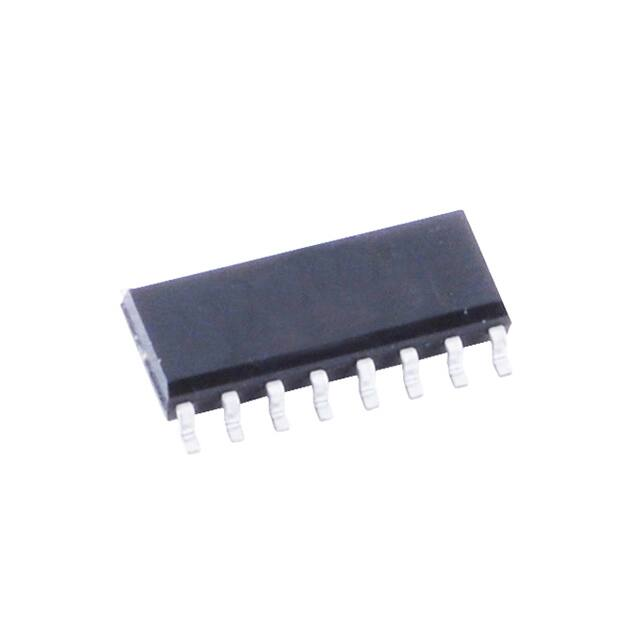
The NTE4511B (16−Lead DIP) and NTE4511BT (SOIC−16) BCD−to−seven segment latch/decoder/drivers are constructed with complementary MOS (CMOS) enhancement mode devices and
NPN bipolar output drivers in a single monolithic structure. The circuit provides the functions of a
4−bit storage latch, an 8421 BCD−to−seven segment decoder, and an output drive capability. Lamp
test (LT), blanking (BI), and latch enable (LE) inputs are used to test the display, to turn−off or pulse
modulate the brightness of the display, and to store a BCD code, respectively. It can be used with
seven−segment light emitting diodes (LED), incandescent, fluorescent, gas discharge, or liquid
crystal readouts either directly or indirectly.
Applications include instrument (e.g., counter, DVM, etc.), display driver, computer/calculator display
driver, cockpit display driver, and various clock, watch, and timer uses.
Features:
D Low Logic Circuit Power Dissipation
D High−Current Sourcing Outputs (Up to 25mA)
D Latching Storage of Code
D Blanking Input
D Lamp Test Provision
D Readout Blanking on All Illegal Input Combinations
D Lamp Intensity Modulation Capability
D Time Share (Multiplexing) Facility
D Supply Voltage Range = 3Vcd to 10Vdc
D Capable of Driving Two Low−Power TTL Loads, One Low−Power Schottky TTL Load or Two
HTL Loads Over the Rated Temperature Range
Absolute Maximum Ratings: (Voltages Referenced to VSS, Note 1)
DC Supply Voltage, VDD . . . . . . . . . . . . . . . . . . . . . . . . . . . . . . . . . . . . . . . . . . . . . . . . . . −0.5 to +18.0V
Input Voltage (All Inputs), Vin . . . . . . . . . . . . . . . . . . . . . . . . . . . . . . . . . . . . . . . . . . . −0.5 to VDD + 0.5V
DC Current Drain (Per Pin), I . . . . . . . . . . . . . . . . . . . . . . . . . . . . . . . . . . . . . . . . . . . . . . . . . . . . . . 10mA
Maximum Output Drive Current (Source) Per Output, IOHmax . . . . . . . . . . . . . . . . . . . . . . . . . . 25mA
Maximum Continuous Output Power (Source) Per Output (Note 2), POHmax . . . . . . . . . . . . . 50mW
Operating Temperature Range, TA . . . . . . . . . . . . . . . . . . . . . . . . . . . . . . . . . . . . . . . . . . −55 to +125°C
Storage Temperature Range, Tstg . . . . . . . . . . . . . . . . . . . . . . . . . . . . . . . . . . . . . . . . . . −65 to +150°C
Note 1. These devices contain circuitry to protect the inputs against damage due to high static
voltages or electric fields; however, it is advised that normal precautions be taken to avoid
application of any voltage higher than maximum rated voltages to this high impedance
circuit. A destructive high current mode may occur if Vin and Vout is not constrained to the
range VSS ≤ (Vin or Vout) ≤ VDD.
Due to the sourcing capability of these circuits, damage can occur to the device if VDD is
applied, and the outputs are shorted to VSS and are at a logical 1 (See Absolute Maximum
Ratings)
Unused inputs must always be tied to an appropriate logic voltage level (e.g., either VSS
or VDD).
Note 2. POHmax = IOH (VDD − VOH)
�Electrical Characteristics: (Voltages referenced to VSS, Note 3)
Parameter
Output Voltage
Vin = VDD or 0
Symbol
“0” Level
VOL
“1” Level
VOH
Vin = 0 or VDD
Input Voltage (Note 5)
“0” Level
(VO = 3.8 or 0.5Vdc)
VIL
−555C
+255C
+1255C
VDD
Vdc
5.0
Min
Max
Min
Typ
Max
Min
Max
−
0.05
−
0
0.05
−
0.05
Unit
Vdc
10
−
0.05
−
0
0.05
−
0.05
Vdc
15
−
0.05
−
0
0.05
−
0.05
Vdc
5.0
4.1
−
4.1
4.57
−
4.1
−
Vdc
10
9.1
−
9.1
9.58
−
9.1
−
Vdc
15
14.1
−
14.1
14.59
−
14.1
−
Vdc
5.0
−
1.5
−
2.25
1.5
−
1.5
Vdc
(VO = 8.8 or 1.0Vdc)
10
−
3.0
−
4.50
3.0
−
3.0
Vdc
(VO = 13.8 or 1.5Vdc)
15
−
4.0
−
6.75
4.0
−
4.0
Vdc
(VO = 0.5 or 3.8Vdc)
“1” Level
VIH
5.0
3.5
−
3.5
2.75
−
3.5
−
Vdc
(VO = 1.0 or 8.8Vdc)
10
7.0
−
7.0
5.50
−
7.0
−
Vdc
(VO = 1.5 or 13.8Vdc)
15
11.0
−
11.0
8.25
−
11.0
−
Vdc
5.0
Output Drive Voltage
(IOH = 0mAdc)
Source
VOH
4.10
−
4.10
4.57
−
4.1
−
Vdc
(IOH = 5.0mAdc)
−
−
−
4.24
−
−
−
Vdc
(IOH = 10mAdc)
3.90
−
3.90
4.12
−
3.5
−
Vdc
(IOH = 15mAdc)
−
−
−
3.94
−
−
−
Vdc
(IOH = 20mAdc)
3.40
−
3.40
3.75
−
3.0
−
Vdc
(IOH = 25mAdc)
−
−
−
3.54
−
−
−
Vdc
9.10
−
9.10
9.58
−
9.1
−
Vdc
(IOH = 5.0mAdc)
−
−
−
9.26
−
−
−
Vdc
(IOH = 10mAdc)
9.00
−
9.00
9.17
−
8.6
−
Vdc
(IOH = 15mAdc)
−
−
−
9.04
−
−
−
Vdc
(IOH = 20mAdc)
8.60
−
8.60
8.90
−
8.2
−
Vdc
(IOH = 25mAdc)
−
−
−
8.75
−
−
−
Vdc
14.1
−
14.1
14.59
−
14.1
−
Vdc
(IOH = 5.0mAdc)
−
−
−
14.27
−
−
−
Vdc
(IOH = 10mAdc)
14.0
−
14.0
14.18
−
13.6
−
Vdc
(IOH = 15mAdc)
−
−
−
14.07
−
−
−
Vdc
(IOH = 20mAdc)
13.6
−
13.6
13.95
−
13.2
−
Vdc
(IOH = 25mAdc)
−
−
−
13.80
−
−
−
Vdc
(IOH = 0mAdc)
(IOH = 0mAdc)
10
15
Note 3. Data labeled “Typ” is not to be used for design purposes but is intended as an indication of
the device’s potential performance.
Note 4. The formulas given are for the typical characteristics only at +25°C.
Note 5. Noise immunity specified for worst−case input combination.
Noise margin for both “1” and “0” = 1.0Vdc min @ VDD = 5Vdc
2.0Vdc min @ VDD = 10Vdc
2.5Vdc min @ VDD = 15Vdc
Note 6. To calculate total supply current at loads other than 50pF:
IT(CL) = IT(50pF) + 3.5 x 10⁻³(CL −50) VDDf
where: IT is in μA (per package), CL in pF, VDD in volts and f in kHz is input frequency.
�Electrical Characteristics (Cont’d): (Voltages referenced to VSS, Note 3)
Parameter
Output Drive Current
(VOL = 0.4Vdc)
Symbol
Sink
IOL
(VOL = 0.5Vdc)
(VOL = 1.5Vdc)
−555C
+255C
+1255C
VDD
Vdc
Min
Max
Min
Typ
Max
Min
Max
Unit
5.0
0.64
−
0.51
0.88
−
0.36
−
mAdc
10
1.6
−
1.3
2.25
−
0.9
−
mAdc
15
4.2
−
3.4
8.8
−
2.4
−
mAdc
Input Current
Iin
15
−
±0.1
−
±0.00001
±0.1
−
±0.1
μAdc
Input Capacitance (VIN = 0)
Cin
−
−
−
−
5.0
7.5
−
−
pF
Quiescent Current
(Per Package)
IDD
5.0
−
5.0
−
0.005
5.0
−
150
μAdc
10
−
10
−
0.010
10
−
300
μAdc
15
−
15
−
0.015
15
−
600
μAdc
Total Supply Current
(Dynamic plus Quiescent,
Per Package, CL = 50pF on
All Outputs, All Buffers
Switching Note 4, Note 6)
IT
5.0
IT = (1.9μA/kHz) f + IDD
μAdc
10
IT = (3.8μA/kHz) f + IDD
μAdc
15
IT = (6.7μA/kHz) f + IDD
μAdc
Note 3. Data labeled “Typ” is not to be used for design purposes but is intended as an indication of
the device’s potential performance.
Note 4. The formulas given are for the typical characteristics only at +25°C.
Note 5. Noise immunity specified for worst−case input combination.
Noise margin for both “1” and “0” = 1.0Vdc min @ VDD = 5Vdc
2.0Vdc min @ VDD = 10Vdc
2.5Vdc min @ VDD = 15Vdc
Note 6. To calculate total supply current at loads other than 50pF:
IT(CL) = IT(50pF) + 3.5 x 10⁻³(CL −50) VDDf
where: IT is in μA (per package), CL in pF, VDD in volts and f in kHz is input frequency.
Switching Characteristics: (CL = 50pF, TA = +25°C, Note 3)
Parameter
Output Rise Time
tTLH = (1.5ns/pf) CL + 50ns
tTLH = (0.75ns/pf) CL + 37.5ns
tTLH = (0.55ns/pf) CL + 37.5ns
Output Fall Time
tTHL = (1.5ns/pf) CL + 50ns
tTHL = (0.75ns/pf) CL + 37.5ns
tTHL = (0.55ns/pf) CL + 37.5ns
Data Propagation Delay Time
tPLH = (0.40ns/pf) CL + 620ns
tPLH = (0.25ns/pf) CL + 237.5ns
tPLH = (0.20ns/pf) CL + 165ns
tPHL = (1.3ns/pf) CL + 655ns
tPHL = (0.60ns/pf) CL + 260ns
tPHL = (0.35ns/pf) CL + 182.5ns
Symbol
tTLH,
tTHL
tPLH
tPHL
VDD
Vdc
Min
Typ
Max
Unit
5.0
10
15
−
−
−
40
30
25
80
60
60
ns
ns
ns
5.0
10
15
−
−
−
125
75
65
250
150
130
ns
ns
ns
5.0
10
15
5.0
10
15
−
−
−
−
−
−
640
250
175
720
290
200
1280
500
350
1440
580
400
ns
ns
ns
ns
ns
ns
Note 3. Data labeled “Typ” is not to be used for design purposes but is intended as an indication of
the device’s potential performance.
Note 4. The formulas given are for the typical characteristics only at +25°C.
�Switching Characteristics (Cont’d): (CL = 50pF, TA = +25°C, Note 3)
VDD
Vdc
Min
Typ
Max
Unit
5.0
−
600
750
ns
tPLH = (0.25ns/pf) CL + 117.5ns
10
−
200
300
ns
tPLH = (0.15ns/pf) CL + 92.5ns
15
−
150
220
ns
5.0
−
485
970
ns
tPHL = (0.45ns/pf) CL + 177.5ns
10
−
200
400
ns
tPHL = (0.35ns/pf) CL + 142.5ns
15
−
160
320
ns
5.0
−
313
625
ns
tPLH = (0.25ns/pf) CL + 112.5ns
10
−
125
250
ns
tPLH = (0.20ns/pf) CL + 80ns
15
−
90
180
ns
5.0
−
313
625
ns
tPHL = (0.45ns/pf) CL + 102.5ns
10
−
125
250
ns
tPHL = (0.35ns/pf) CL + 72.5ns
15
−
90
180
ns
5.0
180
90
−
ns
10
76
38
−
ns
15
40
20
−
ns
5.0
0
−90
−
ns
10
0
−38
−
ns
15
0
−20
−
ns
5.0
520
260
−
ns
10
220
110
−
ns
15
130
65
−
ns
Parameter
Blank Propagation Delay Time
tPLH = (0.30ns/pf) CL + 305ns
tPHL = (0.85ns/pf) CL + 442.5ns
Lamp Test Propagation Delay Time
tPLH = (0.45ns/pf) CL + 290.5ns
tPHL = (1.3ns/pf) CL + 248ns
Setup Time
Hold Time
Latch Enable Pulse Width
Symbol
tPLH
tPHL
tPLH
tPHL
tsu
th
tWL
Note 3. Data labeled “Typ” is not to be used for design purposes but is intended as an indication of
the device’s potential performance.
Note 4. The formulas given are for the typical characteristics only at +25°C.
�Truth Table:
Inputs
Outputs
LE
BI
LT
D
C
B
A
a
b
c
d
e
f
g
X
X
0
X
X
X
X
1
1
1
1
1
1
1
8
X
0
1
X
X
X
X
0
0
0
0
0
0
0
Blank
0
1
1
0
0
0
0
1
1
1
1
1
1
0
0
0
1
1
0
0
0
1
0
1
1
0
0
0
0
1
0
1
1
0
0
1
0
1
1
0
1
1
0
1
2
0
1
1
0
0
1
1
1
1
1
1
0
0
1
3
0
1
1
0
1
0
0
0
1
1
0
0
1
1
4
0
1
1
0
1
0
1
1
0
1
1
0
1
1
5
0
1
1
0
1
1
0
0
0
1
1
1
1
1
6
0
1
1
0
1
1
1
1
1
1
0
0
0
0
7
0
1
1
1
0
0
0
1
1
1
1
1
1
1
8
0
1
1
1
0
0
1
1
1
1
0
0
1
1
9
0
1
1
1
0
1
0
0
0
0
0
0
0
0
Blank
0
1
1
1
0
1
1
0
0
0
0
0
0
0
Blank
0
1
1
1
1
0
0
0
0
0
0
0
0
0
Blank
0
1
1
1
1
0
1
0
0
0
0
0
0
0
Blank
0
1
1
1
1
1
0
0
0
0
0
0
0
0
Blank
0
1
1
1
1
1
1
0
0
0
0
0
0
0
Blank
1
1
1
X
X
X
X
*
*
X = Don’t Care
* Depends upon the BCD code previously applied when LE = 0
Pin Connection Diagram
B 1
16 VDD
C 2
LT 3
15 f
14 g
BI 4
13 a
LE/Strobe 5
12 b
D 6
11 c
A 7
10 d
VSS 8
9 e
Display
a
f
g
e
b
c
d
�NTE4511B
16
9
1
8
.870 (22.0) Max
.260 (6.6)
Max
.200 (5.08)
Max
.100 (2.54)
.099 (2.5) Min
.700 (17.78)
NTE4511BT
.390 (9.9)
16
9
1
8
.050 (1.27)
.236
(5.99)
.154
(3.91)
016 (.406)
061
(1.53)
.006 (.152)
NOTE: Pin1 on Beveled Edge
.198
(5.03)
�


 工商网监
湘ICP备2023018690号
工商网监
湘ICP备2023018690号
