Important notice
Dear Customer,
On 7 February 2017 the former NXP Standard Product business became a new company with the
tradename Nexperia. Nexperia is an industry leading supplier of Discrete, Logic and PowerMOS
semiconductors with its focus on the automotive, industrial, computing, consumer and wearable
application markets
In data sheets and application notes which still contain NXP or Philips Semiconductors references, use
the references to Nexperia, as shown below.
Instead of http://www.nxp.com, http://www.philips.com/ or http://www.semiconductors.philips.com/,
use http://www.nexperia.com
Instead of sales.addresses@www.nxp.com or sales.addresses@www.semiconductors.philips.com, use
salesaddresses@nexperia.com (email)
Replace the copyright notice at the bottom of each page or elsewhere in the document, depending on
the version, as shown below:
- © NXP N.V. (year). All rights reserved or © Koninklijke Philips Electronics N.V. (year). All rights
reserved
Should be replaced with:
- © Nexperia B.V. (year). All rights reserved.
If you have any questions related to the data sheet, please contact our nearest sales office via e-mail
or telephone (details via salesaddresses@nexperia.com). Thank you for your cooperation and
understanding,
Kind regards,
Team Nexperia
�INTEGRATED CIRCUITS
74ALVT16543
2.5 V/3.3 V ALVT 16-bit registered
transceiver (3-State)
Product data sheet
Supersedes data of 1998 Feb 13
�����
�����
����
�
2004 Sep 14
�Philips Semiconductors
Product data sheet
2.5 V/3.3 V 16-bit registered transceiver (3-State)
FEATURES
74ALVT16543
DESCRIPTION
• 16-bit universal bus interface
• 5 V I/O Compatible
• 3-State buffers
• Output capability: +64 mA/–32 mA
• TTL input and output switching levels
• Input and output interface capability to systems at 5 V supply
• Bus-hold data inputs eliminate the need for external pull-up
The 74ALVT16543 is a high-performance BiCMOS product
designed for VCC operation at 2.5 V or 3.3 V with I/O compatibility
up to 5 V. The device can be used as two 8-bit transceivers or one
16-bit transceiver.
The 74ALVT16543 contains two sets of eight D-type latches, with
separate control pins for each set. Using data flow from A to B as an
example, when the A-to-B Enable (nEAB) input and the A-to-B Latch
Enable (nLEAB) input are LOW, the A-to-B path is transparent.
resistors to hold unused inputs
• Live insertion/extraction permitted
• Power-up 3-State
• Power-up reset
• No bus current loading when output is tied to 5 V bus
• Latch-up protection exceeds 500mA per JEDEC Std 17
• ESD protection exceeds 2000 V per MIL STD 883 Method 3015
A subsequent LOW-to-HIGH transition of the nLEAB signal puts the
A data into the latches where it is stored and the B outputs no longer
change with the A inputs. With nEAB and nOEAB both LOW, the
3-State B output buffers are active and display the data present at
the outputs of the A latches.
Control of data flow from B to A is similar, but using the nEBA,
nLEBA, and nOEBA inputs.
and 200 V per Machine Model
Active bus-hold circuitry is provided to hold unused or floating data
inputs at a valid logic level.
QUICK REFERENCE DATA
SYMBOL
TYPICAL
CONDITIONS
Tamb = 25 °C; GND = 0 V
PARAMETER
tPLH
tPHL
Propagation delay
nAx to nBx or nBx to nAx
CL = 50 pF
UNIT
2.5 V
3.3 V
1.8
2.7
1.6
1.8
ns
CIN
Input capacitance DIR, OE
VI = 0 V or VCC
3
3
pF
CI/O
I/O pin capacitance
Outputs disabled; VI/O = 0 V or VCC
9
9
pF
ICCZ
Total supply current
Outputs disabled
40
70
µA
ORDERING INFORMATION
PACKAGES
TEMPERATURE RANGE
TYPE NUMBER
DWG NUMBER
56-Pin Plastic SSOP Type III
–40 °C to +85 °C
74ALVT16543DL
SOT371-1
56-Pin Plastic TSSOP Type II
–40 °C to +85 °C
74ALVT16543DGG
SOT364-1
LOGIC SYMBOL (IEEE/IEC)
56
1EN3 (BA)
29
7EN9 (BA)
54
55
G1
31
G7
1C5
7C11
1
3
2EN4 (AB)
30
28
G2
26
G8
2
2C6
27
8C12
5
∇3
5D
52
15
∇9
11 D
6D
4∇
12 D
10 ∇
6
51
16
41
8
49
17
40
9
48
19
38
10
47
20
37
12
45
21
36
13
44
23
34
14
43
24
33
8EN10 (AB)
42
SW00151
2004 Sep 14
2
�Philips Semiconductors
Product data sheet
2.5 V/3.3 V 16-bit registered transceiver (3-State)
PIN CONFIGURATION
74ALVT16543
LOGIC SYMBOL
5
1OEAB
1
56
1OEBA
1LEAB
2
55
1LEBA
1EAB
3
54
1EBA
GND
4
53
GND
1A0
5
52
1B0
1A1
6
51
7
50
VCC
1A2
8
49
1B2
1A3
9
48
1B3
8
9
10
12
13
14
1A0 1A1 1A2 1A3 1A4 1A5 1A6 1A7
1B1
VCC
6
3
1EAB
54
1EBA
1OEAB
1
2
1LEAB
1OEBA
56
55
1LEBA
1B0 1B1 1B2 1B3 1B4 1B5 1B6 1B7
1A4
10
47
1B4
GND
11
46
GND
1A5
12
45
1B5
1A6
13
44
1B6
1A7
14
43
1B7
26
52
51
49
48
47
45
44
43
15
16
17
19
20
21
23
24
2A0 2A1 2A2 2A3 2A4 2A5 2A6 2A7
2A0
15
42
2B0
2A1
16
41
2B1
31
2EBA
2OEAB
28
2B2
27
2LEAB
2OEBA
29
30
2LEBA
2A2
17
40
GND
18
39
GND
2A3
19
38
2B3
2A4
20
37
2B4
2A5
21
36
2B5
VCC
22
35
VCC
2A6
23
34
2B6
2A7
24
33
2B7
GND
25
32
GND
2EAB
26
31
2EBA
2LEAB
27
30
2LEBA
2OEAB
28
29
2OEBA
2EAB
2B0 2B1 2B2 2B3 2B4 2B5 2B6 2B7
42
41
40
38
37
36
34
33
SH00038
SH00037
PIN DESCRIPTION
PIN NUMBER
SYMBOL
5, 6, 8, 9, 10, 12, 13, 14
15, 16, 17, 19, 20, 21, 23, 24
1A0 – 1A7,
2A0 – 2A7
A Data inputs/outputs
52, 51, 49, 48, 47, 45, 44, 43
42, 41, 40,38, 37, 36, 34, 33
1B0 – 1B7,
2B0 – 2B7
B Data inputs/outputs
1, 56
28, 29
1OEAB, 1OEBA,
2OEAB, 2OEBA
3, 54
26, 31
1EAB, 1EBA,
2EAB, 2EBA
2, 55
27, 30
1LEAB, 1LEBA,
2LEAB, 2LEBA
4, 11, 18, 25, 32, 39, 46, 53
GND
Ground (0 V)
7, 22, 35, 50
VCC
Positive supply voltage
2004 Sep 14
NAME AND FUNCTION
A to B / B to A Output Enable inputs (active-LOW)
A to B / B to A Enable inputs (active-LOW)
A to B / B to A Latch Enable inputs (active-LOW)
3
�Philips Semiconductors
Product data sheet
2.5 V/3.3 V 16-bit registered transceiver (3-State)
74ALVT16543
LOGIC DIAGRAM
DETAIL A
D
nB0
Q
LE
nA0
Q
D
LE
nA1
nB1
nA2
nB2
nA3
nB3
DETAIL A X 7
nA4
nB4
nA5
nB5
nA6
nB6
nA7
nB7
nOEBA
nOEAB
nEBA
nEAB
nLEBA
nLEAB
SH00039
FUNCTION TABLE
INPUTS
H =
h =
L =
l =
X =
↑ =
NC=
Z =
OUTPUTS
STATUS
nOEXX
nEXX
nLEXX
nAx or nBx
nBx or nAx
H
X
X
X
Z
Disabled
X
H
X
X
Z
Disabled
L
L
↑
↑
L
L
h
l
Z
Z
Disabled + Latch
L
L
L
L
↑
↑
h
l
H
L
Latch + Display
L
L
L
L
L
L
H
L
H
L
Transparent
L
L
H
X
NC
Hold
HIGH voltage level
HIGH voltage level one setup time prior to the LOW-to-HIGH transition of nLEXX or nEXX (XX = AB or BA)
LOW voltage level
LOW voltage level one setup time prior to the LOW-to-HIGH transition of nLEXX or nEXX (XX = AB or BA)
Don’t care
LOW-to-HIGH transition of nLEXX or nEXX (XX = AB or BA)
No change
High-impedance or “off ” state
2004 Sep 14
4
�Philips Semiconductors
Product data sheet
2.5 V/3.3 V 16-bit registered transceiver (3-State)
74ALVT16543
ABSOLUTE MAXIMUM RATINGS1, 2
PARAMETER
SYMBOL
VCC
IIK
CONDITIONS
RATING
UNIT
–0.5 to +4.6
V
–50
mA
–0.5 to +7.0
V
VO < 0 V
–50
mA
Output in Off or HIGH state
–0.5 to +7.0
V
Output in LOW state
128
Output in HIGH state
–64
DC supply voltage
DC input diode current
VI < 0 V
voltage3
VI
DC input
IOK
DC output diode current
voltage3
VOUT
DC output
IOUT
DC output
out ut current
Tstg
Storage temperature range
mA
°C
–65 to +150
NOTES:
1. Stresses beyond those listed may cause permanent damage to the device. These are stress ratings only and functional operation of the
device at these or any other conditions beyond those indicated under “recommended operating conditions” is not implied. Exposure to
absolute-maximum-rated conditions for extended periods may affect device reliability.
2. The performance capability of a high-performance integrated circuit in conjunction with its thermal environment can create junction
temperatures which are detrimental to reliability. The maximum junction temperature of this integrated circuit should not exceed 150 °C.
3. The input and output negative voltage ratings may be exceeded if the input and output clamp current ratings are observed.
RECOMMENDED OPERATING CONDITIONS
2.5 V RANGE LIMITS
SYMBOL
VCC
3.3 V RANGE LIMITS
PARAMETER
UNIT
DC supply voltage
MIN
MAX
MIN
MAX
2.3
2.7
3.0
3.6
V
0
5.5
0
5.5
V
VI
Input voltage
VIH
HIGH-level input voltage
VIL
Input voltage
0.7
0.8
V
IOH
HIGH-level output current
–8
–32
mA
LOW-level output current
8
32
LOW-level output current; current duty cycle ≤ 50 %; f ≥ 1 kHz
24
64
∆t/∆v
Input transition rise or fall rate; Outputs enabled
10
10
ns/V
Tamb
Operating free-air temperature range
+85
°C
IOL
2004 Sep 14
1.7
V
mA
–40
5
2.0
+85
–40
�Philips Semiconductors
Product data sheet
2.5 V/3.3 V 16-bit registered transceiver (3-State)
74ALVT16543
DC ELECTRICAL CHARACTERISTICS (3.3 V ± 0.3 V RANGE)
LIMITS
SYMBOL
PARAMETER
VIK
Input clamp voltage
VOH
HIGH-level output
out ut voltage
VOL
VRST
LOW–level output
out ut voltage
Power-up output low voltage6
Temp = –40 °C to +85 °C
TEST CONDITIONS
MIN
TYP1
MAX
–
–0.85
–1.2
VCC – 0.2
VCC
–
VCC = 3.0 V; IOH = –32 mA
2.0
2.3
–
VCC = 3.0 V; IOL = 100 µA
–
0.07
0.2
VCC = 3.0 V; IOL = 16 mA
–
0.25
0.4
VCC = 3.0 V; IOL = 32 mA
–
0.3
0.5
VCC = 3.0 V; IOL = 64 mA
–
0.4
0.55
VCC = 3.6 V; IO = 1 mA; VI = VCC or GND
–
–
0.55
–
0.1
±1
–
0.1
10
–
0.5
1
–
0.1
–5
VCC = 3.6 V; VI = 5.5 V
–
0.1
20
VCC = 0 V; VI or VO = 0 V to 4.5 V
–
0.1
± 100
VCC = 3 V; VI = 0.8 V
75
130
–
VCC = 3 V; VI = 2.0 V
–75
–140
–
± 500
–
–
VCC = 3.0 V; IIK = –18 mA
VCC = 3.0 V to 3.6 V; IOH = –100 µA
VCC = 3.6 V; VI = VCC or GND
Input leakage current
Control pins
VCC = 3.6 V; VI = VCC
VCC = 3.6 V; VI = 0 V
IOFF
IHOLD
Off current
Bus Hold current
uts7
Data in
inputs
Data
pins4
VCC = 0 V to 3.6 V; VCC = 3.6 V
IEX
IPU/PD
V
µA
µA
µA
VO = 5.5 V; VCC = 3.0 V
–
50
125
µA
Power-up/down 3-State output
current3
VCC ≤ 1.2 V; VO = 0.5 V to VCC; VI = GND or VCC;
OE/OE = Don’t care
–
40
± 100
µA
VCC = 3.6 V; Outputs HIGH; VI = GND or VCC;
IO = 0 mA
–
0.07
0.1
VCC = 3.6 V; Outputs LOW; VI = GND or VCC;
IO = 0 mA
–
3.6
5
VCC = 3.6 V; Outputs disabled;
VI = GND or VCC, IO = 0 mA5
–
0.07
0.1
VCC = 3 V to 3.6 V; One input at VCC – 0.6 V;
Other inputs at VCC or GND
–
0.04
0.4
Quiescent supply current
ICCZ
∆ICC
V
Current into an output in the
High state when VO > VCC
ICCH
ICCL
V
V
VCC = 0 V or 3.6 V; VI = 5.5 V
II
UNIT
Additional supply current per
input pin2
mA
mA
NOTES:
1. All typical values are at VCC = 3.3 V and Tamb = 25 °C.
2. This is the increase in supply current for each input at the specified voltage level other than VCC or GND.
3. This parameter is valid for any VCC between 0 V and 1.2 V with a transition time of up to 10 msec. From VCC = 1.2 V to VCC = 3.3 V ± 0.3 V
a transition time of 100 µsec is permitted. This parameter is valid for Tamb = 25 °C only.
4. Unused pins at VCC or GND.
5. ICCZ is measured with outputs pulled up to VCC or pulled down to ground.
6. For valid test results, data must not be loaded into the flip-flops (or latches) after applying power.
7. This is the bus hold overdrive current required to force the input to the opposite logic state.
2004 Sep 14
6
�Philips Semiconductors
Product data sheet
2.5 V/3.3 V 16-bit registered transceiver (3-State)
74ALVT16543
DC ELECTRICAL CHARACTERISTICS (2.5 V ± 0.2 V RANGE)
LIMITS
SYMBOL
PARAMETER
MIN
MAX
–
–0.85
–1.2
VCC – 0.2
VCC
–
VCC = 2.3 V; IOH = –8 mA
1.8
2.1
–
VCC = 2.3 V; IOL = 100 µA
–
0.07
0.2
VCC = 2.3 V; IOL = 24 mA
–
0.3
0.5
VCC = 2.3 V; IOL = 8 mA
–
–
0.4
VCC = 2.7 V; IO = 1 mA; VI = VCC or GND
–
–
0.55
–
0.1
±1
VCC = 0 V or 2.7 V; VI = 5.5 V
–
0.1
10
VCC = 2.7 V; VI = 5.5 V
–
0.1
20
–
0.1
10
VCC = 2.7 V; VI = 0 V
–
0.1
–5
Off current
VCC = 0 V; VI or VO = 0 V to 4.5 V
–
0.1
± 100
Bus Hold current
VCC = 2.3 V; VI = 0.7 V
–
120
–
inputs6
VCC = 2.3 V; VI = 1.7 V
–
–6
–
Current into an output in the
HIGH state when VO > VCC
VO = 5.5 V; VCC = 2.3 V
–
50
125
µA
Power-up/down 3-State output
current3
VCC ≤ 1.2 V; VO = 0.5 V to VCC; VI = GND or VCC;
OE/OE = Don’t care
–
40
100
µA
VCC = 2.7 V; Outputs HIGH, VI = GND or VCC;
IO = 0 mA
–
0.04
0.1
VCC = 2.7 V; Outputs LOW, VI = GND or VCC;
IO = 0 mA
–
2.6
4.5
VCC = 2.7 V; Outputs disabled; VI = GND or VCC;
IO = 0 mA5
–
0.04
0.1
VCC = 2.3 V to 2.7 V; One input at VCC – 0.6 V;
Other inputs at VCC or GND
–
0.01
0.4
Input clamp voltage
VOH
HIGH-level output
out ut voltage
VRST
LOW-level output voltage
Power-up output low voltage7
VCC = 2.3 V; IIK = –18 mA
VCC = 2.3 V to 3.6 V; IOH = –100 µA
VCC = 2.7 V; VI = VCC or GND
II
Input leakage current
IHOLD
Data
IEX
IPU/PD
ICCH
ICCL
Quiescent supply current
ICCZ
∆ICC
Additional supply current per
input pin2
Control pins
Data pins4
VCC = 2.7 V; VI = VCC
IOFF
UNIT
TYP1
VIK
VOL
Temp = –40 °C to +85 °C
TEST CONDITIONS
V
V
V
V
µA
µA
µA
mA
mA
NOTES:
1. All typical values are at VCC = 2.5 V and Tamb = 25 °C.
2. This is the increase in supply current for each input at the specified voltage level other than VCC or GND.
3. This parameter is valid for any VCC between 0 V and 1.2 V with a transition time of up to 10 msec. From VCC = 1.2 V to VCC = 2.5 V ± 0.2 V
a transition time of 100 µsec is permitted. This parameter is valid for Tamb = 25 °C only.
4. Unused pins at VCC or GND.
5. ICCZ is measured with outputs pulled up to VCC or pulled down to ground.
6. Not guaranteed.
7. For valid test results, data must not be loaded into the flip-flops (or latches) after applying power.
2004 Sep 14
7
�Philips Semiconductors
Product data sheet
2.5 V/3.3 V 16-bit registered transceiver (3-State)
74ALVT16543
AC CHARACTERISTICS (3.3 V ± 0.3 V RANGE)
GND = 0 V; tR = tF = 2.5 ns; CL = 50 pF; RL = 500 Ω; Tamb = –40 °C to +85 °C.
LIMITS
SYMBOL
PARAMETER
VCC = 3.3 V ± 0.3 V
WAVEFORM
UNIT
MIN
TYP1
MAX
tPLH
tPHL
Propagation delay
nAx to nBx or nBx to nAx
2
0.5
0.5
1.6
1.8
2.6
3.0
ns
tPLH
tPHL
Propagation delay
nLEBA to nAx, nLEAB to nBx
1
2
1.0
1.0
2.4
2.4
4.0
4.0
ns
tPZH
tPZL
Output enable time
nOEBA to nAx, nOEAB to nBx
4
5
1.0
1.0
2.3
1.8
4.0
3.1
ns
tPHZ
tPLZ
Output disable time
nOEBA to nAx, nOEAB to nBx
4
5
1.0
1.0
3.1
2.7
4.8
4.2
ns
tPZH
tPZL
Output enable time
nEBA to nAx, nEAB to nBx
4
5
1.0
1.0
2.5
1.9
4.2
3.1
ns
tPHZ
tPLZ
Output disable time
nEBA to nAx, nEAB to nBx
4
5
1.0
1.0
2.9
2.4
4.9
4.2
ns
NOTE:
1. All typical values are at VCC = 3.3 V and Tamb = 25 °C.
AC SETUP REQUIREMENTS (3.3 V ± 0.3 V RANGE)
GND = 0 V; tR = tF = 2.5 ns; CL = 50 pF; RL = 500 Ω; Tamb = –40 °C to +85 °C.
LIMITS
SYMBOL
PARAMETER
WAVEFORM
VCC = 3.3 V ± 0.3 V
MIN
TYP
UNIT
ts(H)
ts(L)
Setup time
nAx to nLEAB, nBx to nLEBA
3
0.5
0.7
0
–0.4
ns
th(H)
th(L)
Hold time
nAx to nLEAB, nBx to nLEBA
3
1.5
1.5
0.2
–0.3
ns
ts(H)
ts(L)
Setup time
nAx to nEAB, nBx to nEBA
3
0.5
1.1
–0.3
–0.6
ns
th(H)
th(L)
Hold time
nAx to nEAB, nBx to nEBA
3
1.2
2.0
0.6
0.1
ns
tW(L)
Latch enable pulse width, LOW
3
1.5
–
ns
2004 Sep 14
8
�Philips Semiconductors
Product data sheet
2.5 V/3.3 V 16-bit registered transceiver (3-State)
74ALVT16543
AC CHARACTERISTICS (2.5 V ± 0.2 V RANGE)
GND = 0 V; tR = tF = 2.5 ns; CL = 50 pF; RL = 500 Ω; Tamb = –40 °C to +85 °C.
LIMITS
SYMBOL
PARAMETER
VCC = 2.5 V ± 0.2 V
WAVEFORM
UNIT
MIN
TYP1
MAX
tPLH
tPHL
Propagation delay
nAx to nBx or nBx to nAx
2
1.0
1.0
1.8
2.7
5.1
4.5
ns
tPLH
tPHL
Propagation delay
nLEBA to nAx, nLEAB to nBx
1
2
1.5
1.5
3.9
3.6
6.4
5.9
ns
tPZH
tPZL
Output enable time
nOEBA to nAx, nOEAB to nBx
4
5
1.5
1.5
4.0
2.7
6.5
4.6
ns
tPHZ
tPLZ
Output disable time
nOEBA to nAx, nOEAB to nBx
4
5
1.5
1.5
3.7
2.6
5.6
4.0
ns
tPZH
tPZL
Output enable time
nEBA to nAx, nEAB to nBx
4
5
1.5
1.5
4.2
2.8
7.0
5.0
ns
tPHZ
tPLZ
Output disable time
nEBA to nAx, nEAB to nBx
4
5
1.5
1.5
3.6
2.4
5.6
3.9
ns
NOTE:
1. All typical values are at VCC = 2.5 V and Tamb = 25 °C.
AC SETUP REQUIREMENTS (2.5 V ± 0.2 V RANGE)
GND = 0 V; tR = tF = 2.5 ns; CL = 50 pF; RL = 500 Ω; Tamb = –40 °C to +85 °C.
LIMITS
SYMBOL
PARAMETER
WAVEFORM
VCC = 2.5 V ± 0.2 V
UNIT
MIN
TYP
3
0.5
1.0
–0.2
–0.5
ns
Hold time
nAx to nLEAB, nBx to nLEBA
3
1.0
1.0
0.2
–0.2
ns
ts(H)
ts(L)
Setup time
nAx to nEAB, nBx to nEBA
3
0.5
1.5
–0.3
–0.6
ns
th(H)
th(L)
Hold time
nAx to nEAB, nBx to nEBA
3
1.2
1.5
0
0.2
ns
tW(L)
Latch enable pulse width, LOW
3
1.5
–
ns
ts(H)
ts(L)
Setup time
nAx to nLEAB, nBx to nLEBA
th(H)
th(L)
2004 Sep 14
9
�Philips Semiconductors
Product data sheet
2.5 V/3.3 V 16-bit registered transceiver (3-State)
74ALVT16543
AC WAVEFORMS
For all waveforms VM = 1.5 V or VCC/2, whichever is less.
VIN
VM
3.0 V or VCC
whichever is
less
VM
nOEAB, nOEBA,
nEAB, nEBA
VM
3.0V or VCC
whichever
is less
VM
0V
0V
tPHL
tPZH
tPLH
tPHZ
3.0V or VCC
VOH
VOUT
VM
VM
VM
nAx, nBx
VOL
0V
SW00185
SW00188
Waveform 1. Propagation Delay For Inverting Output
Waveform 4. 3-State Output Enable Time to High Level and
Output Disable Time from High Level
VIN
VM
3.0 V or VCC
whichever is
less
VM
nOEAB, nOEBA,
nEAB, nEBA
0V
tPLH
VM
3.0V or VCC
whichever
is less
VM
0V
tPHL
tPZL
VOH
VOUT
VM
tPLZ
VM
nAx, nBx
VOL
VM
3.0V or VCC
whichever
is less
VOL
SW00186
SW00189
Waveform 2. Propagation Delay For Non-Inverting Output
Waveform 5. 3-State Output Enable Time to Low Level and
Output Disable Time from Low Level
ÉÉÉ
ÉÉÉÉÉÉÉ
ÉÉÉ
ÉÉÉ
ÉÉÉÉÉÉÉ
ÉÉÉ
ÉÉÉ ÉÉÉÉÉÉÉ
ÉÉÉ
nAx,
nBx
VM
VM
VM
3.0V or VCC
whichever
is less
VM
0V
ts(H)
nLEAB, nLEBA,
nEAB, nEBA
th(H)
VM
ts(L)
tw(L)
th(L)
VM
3.0V or VCC
whichever
is less
0V
NOTE: The shaded areas indicate when the input is permitted
to change for predictable output performance.
SW00187
Waveform 3. Data Setup and Hold Times and Latch Enable
Pulse Width
2004 Sep 14
10
�Philips Semiconductors
Product data sheet
2.5 V/3.3 V 16-bit registered transceiver (3-State)
74ALVT16543
TEST CIRCUIT AND WAVEFORMS
6.0V or VCC x 2
VCC
Open
VIN
VOUT
PULSE
GENERATOR
tW
90%
RL
GND
VM
NEGATIVE
PULSE
10%
0V
tTHL (tF)
CL
VIN
VM
10%
D.U.T.
RT
90%
tTLH (tR)
tTLH (tR)
RL
90%
POSITIVE
PULSE
Test Circuit for 3-State Outputs
tTHL (tF)
VIN
90%
VM
VM
10%
10%
tW
0V
SWITCH POSITION
TEST
SWITCH
tPLZ/tPZL
6V or VCC x 2
tPLH/tPHL
Open
tPHZ/tPZH
GND
INPUT PULSE REQUIREMENTS
DEFINITIONS
FAMILY
Amplitude
RL = Load resistor; see AC CHARACTERISTICS for value.
CL = Load capacitance includes jig and probe capacitance:
See AC CHARACTERISTICS for value.
74ALVT16
Rep. Rate
3.0V or VCC
whichever v10MHz
is less
tW
500ns
tR
tF
v2.5ns v2.5ns
RT = Termination resistance should be equal to ZOUT of
pulse generators.
SW00025
2004 Sep 14
11
�Philips Semiconductors
Product data sheet
2.5 V/3.3 V 16-bit registered transceiver (3-State)
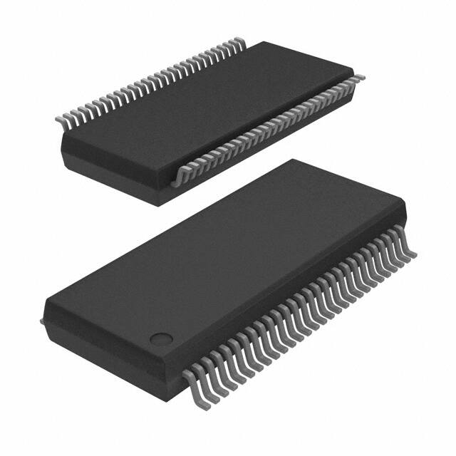
SSOP56: plastic shrink small outline package; 56 leads; body width 7.5 mm
2004 Sep 14
12
74ALVT16543
SOT371-1
�Philips Semiconductors
Product data sheet
2.5 V/3.3 V 16-bit registered transceiver (3-State)
TSSOP56: plastic thin shrink small outline package; 56 leads; body width 6.1 mm
2004 Sep 14
13
74ALVT16543
SOT364-1
�Philips Semiconductors
Product data sheet
2.5 V/3.3 V 16-bit registered transceiver (3-State)
74ALVT16543
REVISION HISTORY
Rev
Date
Description
_3
20040914
Product data sheet (9397 750 14059). Supersedes data of 1998 Feb 13 (9397 750 03568).
Modifications:
• Ordering information table on page 2:
– remove “North America” column; rename third column from “Outside North America” to “Type Number”.
• DC Electrical Characteristics (3.3 V ± 0.3 V range) table on page 6:
– II on Data pins: add condition ‘VCC = 3.6 V; VI = 5.5 V’ and values 0.1 µA (typ) and 20 µA (max).
• AC Characteristics (3.3 V ± 0.3 V range) table on page 8:
– change propagation delay nAx to nBx tPLH Max. time from 2.5 ns to 2.6 ns
– change output disable time nOEBA to nAx, nOEAB to nBx tPHZ (Max.) time from 4.7 ns to 4.8 ns
– change output disable time nOEBA to nAx, nOEAB to nBx tPLZ (Max.) time from 4.0 ns to 4.2 ns
– change output disable time nEBA to nAx, nEAB to nBx tPHZ (Max.) time from 4.5 ns to 4.9 ns
– change output disable time nEBA to nAx, nEAB to nBx tPLZ (Max.) time from 3.8 ns to 4.2 ns
• AC Setup Requirements (3.3 V ± 0.3 V range) table on page 8:
– change setup time nAx to nLEAB, nBx to nLEBA ts(H) (Min.) from 0.0 ns to 0.5 ns; (Typ.) from –0.8 ns to 0 ns
– change setup time nAx to nLEAB, nBx to nLEBA ts(L) (Typ.) from –0.3 ns to –0.4 ns
– change hold time nAx to nLEAB, nBx to nLEBA th(H) (Typ.) from 0.4 ns to 0.2 ns
– change hold time nAx to nLEAB, nBx to nLEBA th(L) (Typ.) from 0.8 ns to –0.3 ns
– change setup time nAx to nEAB, nBx to nEBA ts(H) (Typ.) from –0.8 ns to –0.3 ns
– change setup time nAx to nEAB, nBx to nEBA ts(L) (Typ.) from –0.2 ns to –0.6 ns
– change hold time nAx to nEAB, nBx to nEBA th(H) (Typ.) from 0.3 ns to 0.6 ns
– change hold time nAx to nEAB, nBx to nEBA th(L) (Typ.) from 1.1 ns to 0.1 ns
• AC Setup Requirements (2.5 V ± 0.2 V range) table on page 9:
– change setup time nAx to nLEAB, nBx to nLEBA ts(H) (Min.) from 0 ns to 0.5 ns; (Typ.) from –0.9 ns to –0.2 ns
– change setup time nAx to nLEAB, nBx to nLEBA ts(L) (Typ.) from 0.2 ns to –0.5 ns
– change hold time nAx to nLEAB, nBx to nLEBA th(H) (Min.) from 0.8 ns to 1.0 ns; (Typ.) from –0.2 ns to 0.2 ns
– change hold time nAx to nLEAB, nBx to nLEBA th(L) (Min.) from 1.7 ns to 1.0 ns; (Typ.) from 1.0 ns to –0.2 ns
– change setup time nAx to nEAB, nBx to nEBA ts(H) (Min.) from 0 ns to 0.5 ns; (Typ.) from –1.0 ns to –0.3 ns
– change setup time nAx to nEAB, nBx to nEBA ts(L) (Typ.) from 0.4 ns to –0.6 ns
– change hold time nAx to nEAB, nBx to nEBA th(H) (Min.) from 0.5 ns to 1.2 ns; (Typ.) from 0.2 ns to 0 ns
– change hold time nAx to nEAB, nBx to nEBA th(L) (Min.) from 2.0 ns to 1.5 ns; (Typ.) from 1.3 ns to 0.2 ns
_2
19980213
_1
19951221
2004 Sep 14
Product specification (9397 750 03568). ECN 853-1823 18958 of 13 February 1998.
Supersedes data of 1995 Dec 21.
14
�Philips Semiconductors
Product data sheet
2.5 V/3.3 V 16-bit registered transceiver (3-State)
74ALVT16543
Data sheet status
Level
Data sheet status [1]
Product
status [2] [3]
Definitions
I
Objective data sheet
Development
This data sheet contains data from the objective specification for product development.
Philips Semiconductors reserves the right to change the specification in any manner without notice.
II
Preliminary data sheet
Qualification
This data sheet contains data from the preliminary specification. Supplementary data will be published
at a later date. Philips Semiconductors reserves the right to change the specification without notice, in
order to improve the design and supply the best possible product.
III
Product data sheet
Production
This data sheet contains data from the product specification. Philips Semiconductors reserves the
right to make changes at any time in order to improve the design, manufacturing and supply. Relevant
changes will be communicated via a Customer Product/Process Change Notification (CPCN).
[1] Please consult the most recently issued data sheet before initiating or completing a design.
[2] The product status of the device(s) described in this data sheet may have changed since this data sheet was published. The latest information is available on the Internet at URL
http://www.semiconductors.philips.com.
[3] For data sheets describing multiple type numbers, the highest-level product status determines the data sheet status.
Definitions
Short-form specification — The data in a short-form specification is extracted from a full data sheet with the same type number and title. For detailed information see
the relevant data sheet or data handbook.
Limiting values definition — Limiting values given are in accordance with the Absolute Maximum Rating System (IEC 60134). Stress above one or more of the limiting
values may cause permanent damage to the device. These are stress ratings only and operation of the device at these or at any other conditions above those given
in the Characteristics sections of the specification is not implied. Exposure to limiting values for extended periods may affect device reliability.
Application information — Applications that are described herein for any of these products are for illustrative purposes only. Philips Semiconductors make no
representation or warranty that such applications will be suitable for the specified use without further testing or modification.
Disclaimers
Life support — These products are not designed for use in life support appliances, devices, or systems where malfunction of these products can reasonably be
expected to result in personal injury. Philips Semiconductors customers using or selling these products for use in such applications do so at their own risk and agree
to fully indemnify Philips Semiconductors for any damages resulting from such application.
Right to make changes — Philips Semiconductors reserves the right to make changes in the products—including circuits, standard cells, and/or software—described
or contained herein in order to improve design and/or performance. When the product is in full production (status ‘Production’), relevant changes will be communicated
via a Customer Product/Process Change Notification (CPCN). Philips Semiconductors assumes no responsibility or liability for the use of any of these products, conveys
no license or title under any patent, copyright, or mask work right to these products, and makes no representations or warranties that these products are free from patent,
copyright, or mask work right infringement, unless otherwise specified.
Koninklijke Philips Electronics N.V. 2004
All rights reserved. Published in the U.S.A.
Contact information
For additional information please visit
http://www.semiconductors.philips.com.
Fax: +31 40 27 24825
Date of release: 09-04
For sales offices addresses send e-mail to:
sales.addresses@www.semiconductors.philips.com.
Document number:
�����
�����
����
�
2004 Sep 14
15
9397 750 14059
�