Freescale Semiconductor, Inc.
MOTOROLA
Order number: MC100ES6139
Rev 1, 06/2004
SEMICONDUCTOR TECHNICAL DATA
Freescale Semiconductor, Inc...
3.3V ECL/PECL/HSTL/LVDS ÷2/4,
÷4/5/6 Clock Generation Chip
The MC100ES6139 is a low skew ÷2/4, ÷4/5/6 clock generation chip
designed explicitly for low skew clock generation applications. The internal
dividers are synchronous to each other, therefore, the common output edges
are all precisely aligned. The device can be driven by either a differential or
single-ended ECL or, if positive power supplies are used, LVPECL input
signals. In addition, by using the VBB output, a sinusoidal source can be AC
coupled into the device. If a single-ended input is to be used, the VBB output
should be connected to the CLK input and bypassed to ground via a 0.01 µF
capacitor.
The common enable (EN) is synchronous so that the internal dividers will
only be enabled/disabled when the internal clock is already in the LOW state.
This avoids any chance of generating a runt clock pulse on the internal clock
when the device is enabled/disabled as can happen with an asynchronous
control. The internal enable flip-flop is clocked on the falling edge of the input
clock, therefore, all associated specification limits are referenced to the
negative edge of the clock input.
Upon startup, the internal flip-flops will attain a random state; therefore, for
systems which utilize multiple ES6139s, the master reset (MR) input must be
asserted to ensure synchronization. For systems which only use one ES6139,
the MR pin need not be exercised as the internal divider design ensures
synchronization between the ÷2/4 and the ÷4/5/6 outputs of a single device.
All VCC and VEE pins must be externally connected to power supply to
guarantee proper operation.
The 100ES Series contains temperature compensation.
Features
•
•
•
•
•
•
•
•
•
Maximum Frequency >1.0 GHz Typical
50 ps Output-to-Output Skew
PECL Mode Operating Range: VCC = 3.135 V to 3.8 V with VEE = 0 V
ECL Mode Operating Range: VCC = 0 V with VEE = –3.135 V to –3.8 V
Open Input Default State
Synchronous Enable/Disable
Master Reset for Synchronization of Multiple Chips
VBB Output
LVDS and HSTL Input Compatible
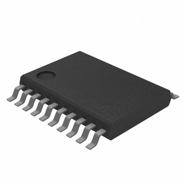
MC100ES6139
SCALE 2 1
DT SUFFIX
20 LEAD TSSOP PACKAGE
CASE 948E-02
DW SUFFIX
20 LEAD SOIC PACKAGE
CASE 751D-06
ORDERING INFORMATION
Device
Package
MC100ES6139DT
TSSOP-20
MC100ES6139DTR2
TSSOP-20
MC100ES6139DW
SO-20
MC100ES6139DWR2
SO-20
© Motorola, Inc. 2004
For More Information On This Product,
Go to: www.freescale.com
�Freescale Semiconductor, Inc.
MC100ES6139
VCC
Q0
Q0
Q1
Q1
Q2
Q2
Q3
Q3
VEE
20
19
18
17
16
15
14
13
12
11
Table 1. Pin Description
Pin
1
CLK , CLK
EN
4
CLK
5
6
CLK
VBB
7
8
MR
9
VCC
10
DIVSELa
3
DIVSELb1
VCC
2
DIVSELb0
1
Figure 1. 20-Lead Pinout (Top View)
Freescale Semiconductor, Inc...
EN1
ECL Sync Enable
MR1
ECL Master Reset
VBB
ECL Reference Output
Q0, Q1, Q0, Q1
ECL Diff ÷2/4 Outputs
Q2, Q3, Q2, Q3
ECL Diff ÷4/5/6 Outputs
DIVSELa
Warning: All VCC and VEE pins must be externally connected to
Power Supply to guarantee proper operation.
Function
ECL Diff Clock Inputs
1
ECL Freq. Select Input ÷2/4
1
DIVSELb01
ECL Freq. Select Input ÷4/5/6
DIVSELb11
ECL Freq. Select Input ÷4/5/6
VCC
ECL Positive Supply
VEE
ECL Negative Supply
1. Pins will default low when left open.
DIVSELa
Q0
CLK
÷2/4
Q0
R
CLK
Q1
Q1
Q2
EN
÷4/5/6
Q2
R
Q3
MR
DIVSELb0
DIVSELb1
Q3
VEE
Figure 2. Logic Diagram
Table 2. Function Tables
CLK
EN
MR
Z
ZZ
X
L
H
X
L
L
H
Function
Divide
Hold Q0:3
Reset Q0:3
X = Don’t Care
Z = Low-to-High Transition
ZZ = High-to-Low Transition
MOTOROLA
DIVSELa
Q0:1 Outputs
L
H
Divide by 2
Divide by 4
DIVSELb0
DIVSELb1
Q2:3 Outputs
L
H
L
H
L
L
H
H
Divide by 4
Divide by 6
Divide by 5
Divide by 5
2
For More Information On This Product,
Go to: www.freescale.com
TIMING SOLUTIONS
�Freescale Semiconductor, Inc.
MC100ES6139
CLK
Q (÷2)
Q (÷4)
Q (÷5)
Q (÷6)
Figure 3. Timing Diagram
CLK
Freescale Semiconductor, Inc...
tRR
RESET
Q (÷n)
Figure 4. Timing Diagram
Table 3. Attributes
Characteristics
Value
Internal Input Pulldown Resistor
75 kΩ
Internal Input Pullup Resistor
75 kΩ
ESD Protection
> 4 kV
> 200 V
> 2 kV
Human Body Model
Machine Model
Charged Device Model
Meets or exceeds JEDEC Spec EIA/JESD78 IC Latchup Test
TIMING SOLUTIONS
3
For More Information On This Product,
Go to: www.freescale.com
MOTOROLA
�Freescale Semiconductor, Inc.
MC100ES6139
Table 4. Maximum Ratings1
Freescale Semiconductor, Inc...
Symbol
Rating
Units
VCC
PECL Mode Power Supply
Parameter
VEE = 0 V
Condition 1
Condition 2
3.9
V
VEE
ECL Mode Power Supply
VCC = 0 V
–3.9
V
VI
PECL Mode Input Voltage
ECL Mode Input Voltage
VEE = 0 V
VCC = 0 V
3.9
–3.9
V
V
Iout
Output Current
Continuous
Surge
50
100
mA
mA
IBB
VBB Sink/Source
± 0.5
mA
TA
Operating Temperature Range
–40 to +85
°C
Tstg
Storage Temperature Range
–65 to +150
°C
θJA
Thermal Resistance (Junction-to-Ambient)
74
64
°C/W
°C/W
TBD
TBD
°C/W
°C/W
VI ≤ VCC
VI ≥ VEE
0 LFPM
500 LFPM
20 TSSOP
20 TSSOP
0 LFPM
500 LFPM
20 SOIC
20 SOIC
1. Maximum Ratings are those values beyond which device damage may occur.
Table 5. DC Characteristics (VCC = 0 V, VEE = –3.8 V to –3.135 V or VCC = 3.135 V to 3.8 V, VEE = 0 V)1
Symbol
Characteristic
–40°C
Min
0°C to 85°C
Typ
Max
35
60
Min
Unit
Typ
Max
35
60
mA
VCC –970
IEE
Power Supply Current
VOH
Output HIGH Voltage2
VCC –1150 VCC –1020
VCC –750
mV
VOL
Output LOW Voltage2
VCC –1950 VCC –1620 VCC –1250 VCC –2000 VCC –1680 VCC –1300
mV
VIH
Input HIGH Voltage (Single-Ended)
VCC –1165
VCC –880
VCC –1165
VCC –880
mV
VIL
Input LOW Voltage (Single-Ended)
VCC –1810
VCC –1475 VCC –1810
VCC –1475
mV
VBB
Output Reference Voltage
VCC –1400
VCC –1200 VCC –1400
VCC –1200
mV
VPP
Voltage3
VCMR
Differential Input
Differential Cross Point
IIH
Input HIGH Current
IIL
Input LOW Current
Voltage4
VCC –800
VCC –1200
0.12
1.3
0.12
1.3
V
VEE +0.2
VCC –1.1
VEE +0.2
VCC –1.1
V
150
µA
150
0.5
0.5
µA
1. MC100ES6139 circuits are designed to meet the DC specifications shown in the above table after thermal equilibrium has been established. The
circuit is in a test socket or mounted on a printed circuit board and transverse airflow greater than 500 lfpm is maintained.
2. All loading with 50 Ω to VCC–2.0 volts.
3. VPP (DC) is the minimum differential input voltage swing required to maintain device functionality.
4. VCMR (DC) is the crosspoint of the differential input signal. Functional operation is obtained when the crosspoint is within the VCMR (DC) range
and the input swing lies within the VPP (DC) specification.
MOTOROLA
4
For More Information On This Product,
Go to: www.freescale.com
TIMING SOLUTIONS
�Freescale Semiconductor, Inc.
MC100ES6139
Table 6. AC Characteristics (VCC = 0 V, VEE = –3.8 V to –3.135 V or VCC = 3.135 V to 3.8 V, VEE = 0 V)1
Symbol
fmax
Maximum Frequency
tPLH,
tPHL
Propagation Delay
tRR
Min
25°C
Typ
Max
Min
Typ
>1
CLK, Q (Diff)
MR, Q
Reset Recovery
85°C
Max
Min
>1
550
400
850
850
Typ
Max
>1
550
400
850
850
550
400
Unit
GHz
850
850
ps
200
100
200
100
200
100
ps
ts
Setup Time
EN, CLK
DIVSEL, CLK
200
400
120
180
200
400
120
180
200
400
120
180
ps
th
Hold Time
CLK, EN
CLK, DIVSEL
100
200
50
140
100
200
50
140
100
200
50
140
ps
MR
550
450
550
450
550
450
ps
tPW
tSKEW
Freescale Semiconductor, Inc...
–40°C
Characteristic
Minimum Pulse Width
Within Device Skew
Q, Q
Q, Q @ Same Frequency
Device-to-Device Skew2
tJITTER
VPP
VCMR
tr
tf
Cycle-to-Cycle Jitter
100
50
300
100
50
300
100
50
300
ps
1
1
1
ps
(RSM 1σ)
Input Voltage Swing (Differential)
Differential Cross Point Voltage
Output Rise/Fall Times
(20% – 80%)
200
1200
VEE+0.2
Q, Q
200
1200
VCC–1.2 VEE+0.2
50
300
200
VCC–1.2 VEE+0.2
50
300
50
1200
mV
VCC–1.2
V
300
ps
1. Measured using a 750 mV source, 50% duty cycle clock source. All loading with 50 Ω to VCC –2.0 V.
2. Skew is measured between outputs under identical transitions. Duty cycle skew is defined only for differential operation when the delays are
measured from the cross point of the inputs to the cross point of the outputs.
Q
D
Receiver
Device
Driver
Device
Q
D
50 Ω
50 Ω
V TT
V TT
=
V CC – 2.0 V
Figure 5. Typical Termination for Output Driver and Device Evaluation
TIMING SOLUTIONS
5
For More Information On This Product,
Go to: www.freescale.com
MOTOROLA
�Freescale Semiconductor, Inc.
MC100ES6139
Marking Notes:
Device Nomenclature
20-Lead TSSOP Marking
MC100ES6139DT
20-Lead SOIC W/B Marking
6139
MC100ES6139DW
MC100ES6139
Trace Code Identification for 20 SOIC: AWLYYWW
“A” - The First character indicates the Assembly location.
“WL” - The Second & Third characters indicate the Source Wafer Lot Tracking Code.
“YY” - The Fourth & Fifth characters indicate the Year device was assembled.
“WW” - The Sixth & Seventh characters indicate the Work Week device was assembled.
Freescale Semiconductor, Inc...
Trace Code Identification for 20 TSSOP: ALYW
“A” - The First character indicates the Assembly location.
“L” - The Second character indicates the Source Wafer Lot Tracking Code.
“Y” - The Third character indicates the “ALPHA CODE” of the year device was assembled.
“W” - The Fourth character indicates the “ALPHA CODE” of the Work Week device was assembled.
The “Y” Year ALPHA CODES
Year
Month
The “W” Work Week ALPHA CODES
Work Week Code
1st 6 Months (WW01 – WW26)
2nd 6 Months (WW27 – WW52)
A = 2003
FIRST 6 MONTHS
WW01 – WW26
A = WW01
A = WW27
B = 2003
SECOND 6 MONTHS
WW27 – WW52
B = WW02
B = WW28
C = 2004
FIRST 6 MONTHS
WW01 – WW26
C = WW03
C = WW29
D = 2004
SECOND 6 MONTHS
WW27 – WW52
D = WW04
D = WW30
E = 2005
FIRST 6 MONTHS
WW01 – WW26
E = WW05
E = WW31
F = 2005
SECOND 6 MONTHS
WW27 – WW52
F = WW06
F = WW32
G = 2006
FIRST 6 MONTHS
WW01 – WW26
G = WW07
G = WW33
H = WW34
H = 2006
SECOND 6 MONTHS
WW27 – WW52
H = WW08
I = 2007
FIRST 6 MONTHS
WW01 – WW26
I = WW09
I = WW35
J = 2007
SECOND 6 MONTHS
WW27 – WW52
J = WW10
J = WW36
K = 2008
FIRST 6 MONTHS
WW01 – WW26
K = WW11
K = WW37
L = 2008
SECOND 6 MONTHS
WW27 – WW52
L = WW12
L = WW38
M = 2009
FIRST 6 MONTHS
WW01 – WW26
M = WW13
M = WW39
N = 2009
SECOND 6 MONTHS
WW27 – WW52
N = WW14
N = WW40
O = 2010
FIRST 6 MONTHS
WW01 – WW26
O = WW15
O = WW41
P = 2010
SECOND 6 MONTHS
WW27 – WW52
P = WW16
P = WW42
Q = 2011
FIRST 6 MONTHS
WW01 – WW26
Q = WW17
Q = WW43
R = 2011
SECOND 6 MONTHS
WW27 – WW52
R = WW18
R = WW44
S = 2012
FIRST 6 MONTHS
WW01 – WW26
S = WW19
S = WW45
T = 2012
SECOND 6 MONTHS
WW27 – WW52
T = WW20
T = WW46
U = 2013
FIRST 6 MONTHS
WW01 – WW26
U = WW21
U = WW47
V = 2013
SECOND 6 MONTHS
WW27 – WW52
V = WW22
V = WW48
W = 2014
FIRST 6 MONTHS
WW01 – WW26
W = WW23
W = WW49
X = 2014
SECOND 6 MONTHS
WW27 – WW52
X = WW24
X = WW50
Y = 2015
FIRST 6 MONTHS
WW01 – WW26
Y = WW25
Y = WW51
Z = 2015
SECOND 6 MONTHS
WW27 – WW52
Z = WW26
Z = WW52
20 TSSOP Tracecode Marking Example:
5ABR
5
= Assembly Location
A
= First Lot Assembled of this device in the designated
Work Week
B = 2003 Second 6 Months, WW27 - WW52
R= WW44 of 2003
MOTOROLA
6
For More Information On This Product,
Go to: www.freescale.com
TIMING SOLUTIONS
�Freescale Semiconductor, Inc.
MC100ES6139
OUTLINE DIMENSIONS
DT SUFFIX
20 LEAD TSSOP PACKAGE
CASE 948E-02
ISSUE A
20X
0.15 (0.006) T U
K REF
0.10 (0.004)
S
M
T U
V
S
S
NOTES:
1. DIMENSIONING AND TOLERANCING PER ANSI
Y14.5M, 1982.
2. CONTROLLING DIMENSION: MILLIMETER.
3. DIMENSION A DOES NOT INCLUDE MOLD
FLASH, PROTRUSIONS OR GATE BURRS. MOLD
FLASH OR GATE BURRS SHALL NOT EXCEED
0.15 (0.006) PER SIDE.
4. DIMENSION B DOES NOT INCLUDE INTERLEAD
FLASH OR PROTRUSION. INTERLEAD FLASH
OR PROTRUSION SHALL NOT EXCEED 0.25
(0.010) PER SIDE.
5. DIMENSION K DOES NOT INCLUDE DAMBAR
PROTRUSION. ALLOWABLE DAMBAR
PROTRUSION SHALL BE 0.08 (0.003) TOTAL IN
EXCESS OF THE K DIMENSION AT MAXIMUM
MATERIAL CONDITION.
6. TERMINAL NUMBERS ARE SHOWN FOR
REFERENCE ONLY.
7. DIMENSION A AND BE ARE TO BE DETERMINED
AT DATUM PLANE -W-.
K
K1
2X
L/2
20
11
PIN 1
IDENT
Freescale Semiconductor, Inc...
J J1
B
-U-
L
SECTION N-N
10
0.25 (0.010)
N
0.15 (0.006) T U
S
M
A
-VN
F
DETAIL E
-W-
C
D
G
H
DETAIL E
0.100 (0.004)
–T–
SEATING
PLANE
DIM
A
B
C
D
F
G
H
J
J1
K
K1
L
M
MILLIMETERS
MIN MAX
6.40
6.60
4.30
4.50
--1.20
0.05
0.15
0.50
0.75
0.65 BSC
0.27
0.37
0.09
0.20
0.09
0.16
0.19
0.30
0.19
0.25
6.40 BSC
0˚
8˚
INCHES
MIN MAX
0.252 0.260
0.169 0.177
0.047
--0.002 0.006
0.020 0.030
0.026 BSC
0.011 0.015
0.004 0.008
0.004 0.006
0.007 0.012
0.007 0.010
0.252 BSC
8˚
0˚
CASE 948E-02
ISSUE A
DATE 12/04/94
TIMING SOLUTIONS
7
For More Information On This Product,
Go to: www.freescale.com
MOTOROLA
�Freescale Semiconductor, Inc.
MC100ES6139
OUTLINE DIMENSIONS
DW SUFFIX
20 LEAD SOIC PACKAGE
CASE 751D-06
ISSUE H
10X
PIN
NUMBER
10.55
10.05
0.25 M B
2.65
2.35
0.25
0.10
A
20X
1
20
Freescale Semiconductor, Inc...
PIN 1 INDEX
0.49
0.35
0.25
6
M
T A B
18X
1.27
A
10
4 12.95
12.65
A
11
T
SEATING PLANE
20X
7.6
7.4
0.1 T
B
5
0.75 X45˚
0.25
0.32
0.23
1.0
0.4
7˚
0˚
NOTES:
1. DIMENSIONS ARE IN MILLIMETERS.
2. DIMENSIONING AND TOLERANCING PER
ASME Y14.5M, 1994.
3. DATUMS A AND B TO BE DETERMINED AT THE
PLANE WHERE THE BOTTOM OF THE LEADS
EXIT THE PLASTIC BODY.
4. THIS DIMENSION DOES NOT INCLUDE MOLD
FLASH, PROTRUSION OR GATE BURRS. MOLD
FLASH, PROTRUSION OR GATE BURRS SHALL
NOT EXCEED 0.15 MM PER SIDE. THIS DIMENSION
IS DETERMINED AT THE PLANE WHERE THE
BOTTOM OF THE LEADS EXIT THE PLASTIC BODY.
5. THIS DIMENSION DOES NOT INCLUDE INTER-LEAD
FLASH OR PROTRUSIONS. INTER-LEAD FLASH
AND PROTRUSIONS SHALL NOT EXCEED 0.25 MM
PER SIDE. THIS DIMENSION IS DETERMINED AT
THE PLANE WHERE THE BOTTOM OF THE LEADS
EXIT THE PLASTIC BODY.
6. THIS DIMENSION DOES NOT INCLUDE DAMBAR
PROTRUSION. ALLOWABLE DAMBAR PROTRUSION
SHALL NOT CAUSE WIDTH TO EXCEED 0.62 MM.
SECTION A-A
CASE 751D-06
ISSUE H
DATE 03/05/02
MOTOROLA
8
For More Information On This Product,
Go to: www.freescale.com
TIMING SOLUTIONS
�Freescale Semiconductor, Inc.
MC100ES6139
Freescale Semiconductor, Inc...
NOTES
TIMING SOLUTIONS
9
For More Information On This Product,
Go to: www.freescale.com
MOTOROLA
�Freescale Semiconductor, Inc.
MC100ES6139
Freescale Semiconductor, Inc...
NOTES
MOTOROLA
10
For More Information On This Product,
Go to: www.freescale.com
TIMING SOLUTIONS
�Freescale Semiconductor, Inc.
MC100ES6139
Freescale Semiconductor, Inc...
NOTES
TIMING SOLUTIONS
11
For More Information On This Product,
Go to: www.freescale.com
MOTOROLA
�Freescale Semiconductor, Inc...
Freescale Semiconductor, Inc.
Information in this document is provided solely to enable system and software implementers to use Motorola products. There are no express or implied
copyright licenses granted hereunder to design or fabricate any integrated circuits or integrated circuits based on the information in this document.
Motorola reserves the right to make changes without further notice to any products herein. Motorola makes no warranty, representation or guarantee
regarding the suitability of its products for any particular purpose, nor does Motorola assume any liability arising out of the application or use of any product
or circuit, and specifically disclaims any and all liability, including without limitation consequential or incidental damages. “Typical” parameters which may be
provided in Motorola data sheets and/or specifications can and do vary in different applications and actual performance may vary over time. All operating
parameters, including “Typicals” must be validated for each customer application by customer’s technical experts. Motorola does not convey any license
under its patent rights nor the rights of others. Motorola products are not designed, intended, or authorized for use as components in systems intended for
surgical implant into the body, or other applications intended to support or sustain life, or for any other application in which the failure of the Motorola product
could create a situation where personal injury or death may occur. Should Buyer purchase or use Motorola products for any such unintended or
unauthorized application, Buyer shall indemnify and hold Motorola and its officers, employees, subsidiaries, affiliates, and distributors harmless against all
claims, costs, damages, and expenses, and reasonable attorney fees arising out of, directly or indirectly, any claim of personal injury or death associated
with such unintended or unauthorized use, even if such claim alleges that Motorola was negligent regarding the design or manufacture of the part.
MOTOROLA and the Stylized M Logo are registered in the US Patent and Trademark Office. All other product or service names are the property of their
respective owners.
© Motorola, Inc. 2004
HOW TO REACH US:
USA/EUROPE/LOCATIONS NOT LISTED:
Motorola Literature Distribution
P.O. Box 5405, Denver, Colorado 80217
1-800-521-6274 or 480-768-2130
JAPAN: Motorola Japan Ltd.; SPS, Technical Information Center
3-20-1 Minami-Azabu. Minato-ku, Tokyo 106-8573, Japan
81-3-3440-3569
ASIA/PACIFIC: Motorola Semiconductors H.K. Ltd.; Silicon Harbour Centre
2 Dai King Street, Tai Po Industrial Estate, Tai Po, N.T., Hong Kong
852-26668334
HOME PAGE: http://motorola.com/semiconductors
MC100ES6139
For More Information On This Product,
Go to: www.freescale.com
�


 工商网监
湘ICP备2023018690号
工商网监
湘ICP备2023018690号
