MC33926
5.0 A throttle control H-bridge
Rev. 16 — 19 February 2020
1
Data sheet: technical data
General description
The 33926 is a SMARTMOS monolithic H-bridge power IC designed primarily for
automotive electronic throttle control, but is applicable to any low-voltage DC servo motor
control application within the current and voltage limits stated in this specification. It
meets the stringent requirements of automotive applications and is fully AEC-Q100 grade
1 qualified.
The 33926 is able to control inductive loads with currents up to 5.0 A peak. RMS current
capability is subject to the degree of heatsinking provided to the device package. Internal
peak-current limiting (regulation) is activated at load currents above 6.5 A ±1.5 A. Output
loads can be pulse width modulated (PWM’ed) at frequencies up to 20 kHz. A load
current feedback feature provides a proportional (0.24 % of the load current) current
output suitable for monitoring by a microcontroller’s A/D input. A status flag output reports
undervoltage, overcurrent, and overtemperature fault conditions.
Two independent inputs provide polarity control of two half-bridge totem-pole outputs.
Two independent disable inputs are provided to force the H-bridge outputs to tri-state
(high-impedance off state). An inverted input changes the IN1 and IN2 inputs to low (true
logic).
2
Simplified application diagram
VDD
VPWR
VPWR
SF
FB
CCP
IN1
OUT1
IN2
MCU
INV
SLEW
D1
D2
EN
33926
motor
OUT2
PGND
AGND
aaa-028113
Figure 1. Simplified application diagram
3
Features and benefits
• 5.0 V to 28 V continuous operation (transient operation from 5.0 V to 40 V)
�MC33926
NXP Semiconductors
5.0 A throttle control H-bridge
•
•
•
•
•
•
•
225 mΩ maximum RDS(on) at 150 °C (each H-bridge MOSFET)
3.0 V and 5.0 V TTL/CMOS logic compatible inputs
Overcurrent limiting (regulation) via an internal constant-off-time PWM
Output short-circuit protection (short to VPWR or ground)
Temperature dependent current limit threshold reduction
All inputs have an internal source/sink to define the default (floating input) states
Sleep mode with current draw < 50 µA (with inputs floating or set to match default logic
states)
• AEC-Q100 grade 1 qualified
4
Applications
•
•
•
•
5
Electronic throttle control (ETC)
Exhaust gas recirculation (EGR)
Turbo flap control
Industrial and medical pumps and motor control
Ordering information
This section describes the part numbers available to be purchased along with their
differences. Valid orderable part numbers are provided on the web. To determine the
orderable part numbers for this device, go to http://www.nxp.com and perform a part
number search.
Table 1. Orderable parts
Part number
[1]
Operating temperature
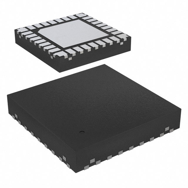
MC33926PNB
MC33926AES
[1]
MC33926
Data sheet: technical data
Package
32-pin PQFN
TA = −40 °C to 125 °C
28-pin HVQFN with inspectable
fillets
To order parts in tape and reel, add the R2 suffix to the part number.
All information provided in this document is subject to legal disclaimers.
Rev. 16 — 19 February 2020
© NXP B.V. 2020. All rights reserved.
2 / 35
�MC33926
NXP Semiconductors
5.0 A throttle control H-bridge
6
Internal block diagram
VPWR
VDD
LOGIC SUPPLY
CCP
VCP
HS1
CHARGE
PUMP
HS2
OUT1
OUT2
EN
IN1
LS1
IN2
D2
D1
INV
SLEW
LS1
HS1
to gates
HS2
GATE DRIVE
AND
PROTECTION
LOGIC
LS2
PGND
LS2
VSENSE
SF
CURRENT MIRROR
AND
CONSTANT OFF-TIME
PWM CURRENT REGULATOR
ILIM PWM
FB
AGND
PGND
aaa-028114
Figure 2. Internal block diagram
7
Pinning information
IN2
1
32 31 30
D1
OUT2
OUT2
OUT2
OUT2
VPWR
CCP
7.1 Pinning
29 28 27 26
25
n.c.
IN1
2
24
PGND
SLEW
3
23
PGND
VPWR
4
22
PGND
AGND
AGND
5
21
SF
VPWR
6
20
PGND
INV
7
19
PGND
FB
8
18
PGND
n.c.
9
17
n.c.
Transparent top view
D2
OUT1
OUT1
13 14 15 16
OUT1
OUT1
VPWR
EN
10 11 12
aaa-028115
Figure 3. Pin configuration for 32-pin PQFN
MC33926
Data sheet: technical data
All information provided in this document is subject to legal disclaimers.
Rev. 16 — 19 February 2020
© NXP B.V. 2020. All rights reserved.
3 / 35
�MC33926
NXP Semiconductors
D1
AGND
AGND
22
OUT2
23
VPWR
OUT2
24
25
VPWR
26
CCP
27
28
AGND
IN2
terminal 1
index area
AGND
5.0 A throttle control H-bridge
n.c.
1
21
n.c.
IN1
2
20
PGND
SLEW
3
19
PGND
18
SF
AGND
Transparent top view
AGND
AGND
14
AGND
AGND
D2
n.c.
13
15
OUT1
7
11
PGND
12
16
OUT1
6
VPWR
FB
n.c.
10
PGND
VPWR
17
9
5
EN
INV
8
4
n.c.
AGND
aaa-028116
Figure 4. Pin configuration for 28-pin HVQFN
7.2 Pin description
For functional description of each pin see Section 9.2 "Functional pin description".
Table 2. Pin description
32-pin PQFN
28-pin QFN
Pin name
Pin function
Formal name
Definition
1
28
IN2
Logic input
Input 2
Logic input control of OUT2; example, when IN2
is logic high, OUT2 is set to VPWR, and when
IN2 is logic low, OUT2 is set to PGND (Schmitt
trigger input with ~ 80 µA source so default
condition = OUT2 high)
2
2
IN1
Logic input
Input 1
Logic input control of OUT1; example, when IN1
is logic high, OUT1 is set to VPWR, and when
IN1 is logic low, OUT1 is set to PGND (Schmitt
trigger input with ~ 80 µA source so default
condition = OUT1 high)
3
3
SLEW
Logic input
Slew rate
Logic input to select fast or slow slew rate
(Schmitt trigger input with ~ 80 µA sink so
default condition = slow)
4, 6, 11, 31
10, 11, 25, 26
VPWR
Power input
Positive power
supply
These pins must be connected together
physically as close as possible and directly
soldered down to a wide, thick, low resistance
supply plane on the PCB.
5, Exposed Pad
4, Exposed pad
AGND
Analog ground
Analog signal
ground
The low current analog signal ground must be
connected to PGND via low-impedance path
(
很抱歉,暂时无法提供与“MC33926PNB”相匹配的价格&库存,您可以联系我们找货
免费人工找货