NXP Semiconductors
Data Sheet: Technical Data
Document Number: IMX7SCEC
Rev. 6, 03/2019
MCIMX7SxDxxxxxD
MCIMX7SxExxxxxD
i.MX 7Solo Family of
Applications Processors
Datasheet
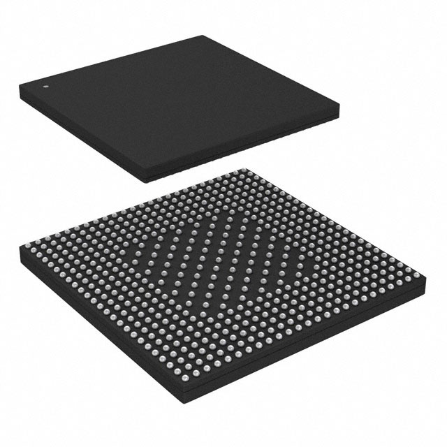
Package Information
Plastic Package
BGA 12 x 12 mm, 0.4 mm pitch
BGA 19 x 19 mm, 0.75 mm pitch
Ordering Information
See Table 1 on page 3
1
i.MX 7Solo introduction
The i.MX 7Solo family of processors represents NXP’s
latest achievement in high-performance processing for
low-power requirements with a high degree of functional
integration. These processors are targeted towards the
growing market of connected and portable devices.
The i.MX 7Solo family of processors features advanced
implementation of the Arm® Cortex®-A7 core, which
operates at speeds of up to 800 MHz. The i.MX 7Solo
family provides up to 32-bit
DDR3/DDR3L/LPDDR2/LPDDR3-1066 memory
interface and a number of other interfaces for connecting
peripherals, such as WLAN, Bluetooth, GPS, displays,
and camera sensors.
1
2
3
4
5
6
7
i.MX 7Solo introduction . . . . . . . . . . . . . . . . . . . . . . . . . . . 1
1.1 Ordering information . . . . . . . . . . . . . . . . . . . . . . . . 3
1.2 Features . . . . . . . . . . . . . . . . . . . . . . . . . . . . . . . . . 4
Architectural overview . . . . . . . . . . . . . . . . . . . . . . . . . . . . 8
2.1 Block diagram . . . . . . . . . . . . . . . . . . . . . . . . . . . . . 8
Modules list . . . . . . . . . . . . . . . . . . . . . . . . . . . . . . . . . . . . 9
3.1 Special signal considerations . . . . . . . . . . . . . . . . 15
3.2 Recommended connections for unused analog
interfaces. . . . . . . . . . . . . . . . . . . . . . . . . . . . . . . . 18
Electrical characteristics . . . . . . . . . . . . . . . . . . . . . . . . . 19
4.1 Chip-level conditions . . . . . . . . . . . . . . . . . . . . . . . 19
4.2 Integrated LDO voltage regulator parameters . . . . 34
4.3 PLL electrical characteristics. . . . . . . . . . . . . . . . . 36
4.4 On-chip oscillators. . . . . . . . . . . . . . . . . . . . . . . . . 36
4.5 I/O DC parameters . . . . . . . . . . . . . . . . . . . . . . . . 37
4.6 I/O AC parameters . . . . . . . . . . . . . . . . . . . . . . . . 41
4.7 Output buffer impedance parameters . . . . . . . . . . 45
4.8 System modules timing . . . . . . . . . . . . . . . . . . . . . 47
4.9 General-purpose media interface (GPMI) timing. . 67
4.10 External peripheral interface parameters . . . . . . . 75
4.11 12-Bit A/D converter (ADC) . . . . . . . . . . . . . . . . . 112
Boot mode configuration . . . . . . . . . . . . . . . . . . . . . . . . 113
5.1 Boot mode configuration pins . . . . . . . . . . . . . . . 113
5.2 Boot device interface allocation. . . . . . . . . . . . . . 114
Package information and contact assignments. . . . . . . 116
6.1 12 x 12 mm package information . . . . . . . . . . . . 116
6.2 19 x 19 mm package information . . . . . . . . . . . . 134
Release notes . . . . . . . . . . . . . . . . . . . . . . . . . . . . . . . . 151
NXP reserves the right to change the detail specifications as may be required to permit improvements in the design of
its products.
© 2016, 2017, 2019 NXP B.V.
�i.MX 7Solo introduction
The i.MX 7Solo family of processors is specifically useful for applications such as:
• Audio
• Connected devices
• Access control panels
• Human-machine interfaces (HMI)
• Portable medical and health care
• IP phones
• Smart appliances
• Point of Sale
• eReaders
• Wearables
• Home energy management systems
The features of the i.MX 7Solo family of processors include the following:
• Arm Cortex-A7 plus Arm Cortex-M4—Heterogeneous Multicore Processing architecture enables
the device to run an open operating system like Linux/Android on the Cortex-A7 core and an RTOS
like FreeRTOS™ on the Cortex-M4 core.
• Arm Cortex-A7 core—The processor enhances the capabilities of portable, connected applications
by fulfilling the ever-increasing MIPS needs of operating systems and applications at lowest power
consumption levels per MHz.
• Multilevel memory system—The multilevel Cortex-A7 memory system is based on the L1
instruction and data caches, L2 cache, and internal and external memory. The processor supports
many types of external memory devices, including DDR3, DDR3L, LPDDR2 and LPDDR3, NOR
Flash, NAND Flash (MLC and SLC), QSPI Flash, and managed NAND, including eMMC rev.
• Power efficiency—Power management implemented throughout the IC enables features and
peripherals to consume minimum power in both active and various low-power modes.
• Multimedia—The multimedia performance is enhanced by a multilevel cache system, NEON™
MPE (Media Processor Engine) coprocessor, a programmable smart DMA (SDMA) controller.
• Gigabit Ethernet with AVB—10/100/1000 Mbps Ethernet controllers supporting IEEE Std 1588
time synchronization.
• Human-machine interface (HMI)—i.MX 7Solo processor provides up to two separate display
interfaces (parallel display and two-lane MIPI-DSI), CMOS sensor interface (two-lane MIPI-CSI
and parallel).
• Interface flexibility—i.MX 7Solo processor supports connections to a variety of interfaces: one
high-speed USB on-the-go module with PHY, High-Speed Inter-Chip USB, multiple expansion
card ports (high-speed MMC/SDIO host and other), a Gigabit Ethernet controller with support for
Ethernet AVB, two 12-bit ADCs with a total of 8 single-ended inputs, two CAN ports, and a variety
of other popular interfaces (such as UART, I2C, and I2S).
• Advanced security—The processors deliver hardware-enabled security features that enable secure
e-commerce, digital rights management (DRM), information encryption, secure boot, and secure
i.MX 7Solo Family of Applications Processors Datasheet, Rev. 6, 02/2019
2
NXP Semiconductors
�i.MX 7Solo introduction
•
software downloads. The security features are discussed in detail in the i.MX 7Dual security
reference manual.
Integrated power management—The processors integrate linear regulators and internally generate
voltage levels for different power domains. This significantly simplifies system power
management structure.
For a comprehensive list of the i.MX 7Solo features, see Section 1.2, “Features.”
1.1
Ordering information
Table 1 provides examples of orderable sample part numbers covered by this data sheet.
Table 1. Orderable parts
1
2
Cortex-A7 CPU
Qualification Tier
Speed Grade
Temperature
(Tj)
Part Number
Options
MCIMX7S5EVM08SD
CAN,
1 x Gb ETH
10 tamper pins
2 x ADC
800 MHz
Industrial1
-20 to +105°C
19x19 mm
0.75mm pitch
BGA
MCIMX7S3DVK08SD
No CAN,
1 x Gb ETH
4 tamper pins
1 x ADC
800 MHz
Consumer2
0 to +95°C
12x12 mm
0.4 mm pitch
BGA
MCIMX7S5EVK08SD
CAN
1 x Gb ETH
4 tamper pins
1 x ADC
800 MHz
Industrial1
–20 to +105°C 12x12 mm
0.4 mm pitch
BGA
MCIMX7S3EVK08SD
No CAN
1 x Gb ETH
4 tamper pins
1 x ADC
800 MHz
Industrial1
–20 to +105°C 12x12 mm
0.4 mm pitch
BGA
Package
Industrial qualification grade assumes 10-year lifetime with 100% duty cycle.
Consumer qualification grade assumes 5-year lifetime with 50% duty cycle.
i.MX 7Solo Family of Applications Processors Datasheet, Rev. 6, 02/2019
NXP Semiconductors
3
�i.MX 7Solo introduction
Figure 1 describes the part number nomenclature so that the users can identify the characteristics of the
specific part number.
Figure 1. Part number nomenclature—i.MX 7Solo family of processors
1.2
Features
The i.MX 7Solo family of processors is based on Arm Cortex-A7 MPCore™ Platform, which has the
following features:
• Arm Cortex-A7 Core (with TrustZone® technology)
• The core includes:
— 32 KByte L1 Instruction Cache
— 32 KByte L1 Data Cache
— Private Timer and Watchdog
— NEON MPE (media processing engine) coprocessor
The Arm Cortex-A7 Core complex shares:
• General interrupt controller (GIC) with 128 interrupt support
• Global timer
• Snoop control unit (SCU)
• 512 KB unified I/D L2 cache
• Two master AXI bus interfaces output of L2 cache
i.MX 7Solo Family of Applications Processors Datasheet, Rev. 6, 02/2019
4
NXP Semiconductors
�i.MX 7Solo introduction
•
•
Frequency of the core (including NEON and L1 cache), as per Table 9.
NEON MPE coprocessor
— SIMD Media Processing Architecture
— NEON register file with 32x64-bit general-purpose registers
— NEON Integer execute pipeline (ALU, Shift, MAC)
— NEON dual, single-precision floating point execute pipeline (FADD, FMUL)
— NEON load/store and permute pipeline
The Arm Cortex-M4 platform:
• Cortex-M4 CPU core
• MPU (memory protection unit)
• FPU (floating-point unit)
• 16 KByte instruction cache
• 16 KByte data cache
• 64 KByte TCM (tightly-coupled memory)
The SoC-level memory system consists of the following additional components:
— Boot ROM, including HAB (96 KB)
— Internal multimedia / shared, fast access RAM (256 KB of total OCRAM)
— Secure/nonsecure RAM (32 KB)
• External memory interfaces: The i.MX 7Solo family of processors supports the latest,
high-volume, cost effective DRAM, NOR, and NAND Flash memory standards.
— Up to 32-bit LP-DDR2-1066, DDR3-1066, DDR3L-1066, and LPDDR3-1066
— 8-bit NAND-Flash, including support for Raw MLC/SLC, 2 KB, 4 KB, and 8 KB page size,
BA-NAND, PBA-NAND, LBA-NAND, OneNAND™ and others. BCH ECC up to 62 bits.
— 16/32-bit NOR Flash. All EIMv2 pins are muxed on other interfaces.
Each i.MX 7Solo processor enables the following interfaces to external devices (some of them are muxed
and not available simultaneously):
• Displays—Available interfaces.
— One parallel 24-bit display port
— One MIPI DSI port
• Camera sensors:
— One parallel Camera port (up to 24 bit and up to 133 MHz peak)
— One MIPI-CSI port
• Expansion cards:
— Three MMC/SD/SDIO card ports all supporting the following. Moreover, the third port can
support HS400.
– 1-bit or 4-bit transfer mode specifications for SD and SDIO cards, up to 208 MHz
i.MX 7Solo Family of Applications Processors Datasheet, Rev. 6, 02/2019
NXP Semiconductors
5
�i.MX 7Solo introduction
•
•
– 1-bit, 4-bit, or 8-bit transfer mode specifications for MMC cards up to 200 MHz in both
SDR and DDR modes, including HS200 and HS400 DDR modes
USB:
— One high-speed (HS) USB 2.0 OTG (Up to 480 Mbps), with integrated HS USB PHY
— One high-speed USB 2.0 (480 Mbps) host with integrated HSIC USB (high-speed inter-chip
USB) PHY
Miscellaneous IPs and interfaces:
— Three instances of SAI supporting up to three I2S and AC97 ports
— Seven UARTs, up to 4.0 Mbps:
– Providing RS232 interface
– Supporting 9-bit RS485 Multidrop mode
— Four eCSPI (Enhanced CSPI)
— Four I2C, supporting 400 kbps
— 1-gigabit Ethernet controller (designed to be compatible with IEEE Std 1588), 10/100/1000
Mbps with AVB support
— Four pulse width modulators (PWM)
— System JTAG controller (SJC)
— GPIO with interrupt capabilities
— 8x8 key pad port (KPP)
— One quad SPI
— Four watchdog timers (WDOG)
— One (12 x 12 mm) or two (19 x 19 mm) 2-channel, 12-bit analog-to-digital converters
(ADC)—effective number of bits (ENOB) can vary (typically 9–10 bits) depending on the
system implementation and the condition of the power/ground noise condition
The i.MX 7Solo family of processors integrates advanced power management unit and controllers:
• PMU (power-management unit), multiple LDO supplies, for on-chip resources
• Temperature sensor for monitoring the die temperature
• Software state retention and power gating for Arm and NEON
• Support for various levels of system power modes
• Flexible clock gating control scheme
The i.MX 7Solo family of processors uses dedicated hardware accelerators to meet the targeted
multimedia performance. The use of hardware accelerators is a key factor in obtaining high performance
at low power consumption numbers, while having the CPU core relatively free for performing other tasks.
The i.MX 7Solo family of processors incorporates the following hardware accelerators:
• PXP—PiXel processing pipeline for imagine resize, rotation, overlay and CSC. Off loading key
pixel processing operations are required to support the LCD.
Security functions are implemented by the following hardware:
• Arm TrustZone technology including separation of interrupts and memory mapping
i.MX 7Solo Family of Applications Processors Datasheet, Rev. 6, 02/2019
6
NXP Semiconductors
�i.MX 7Solo introduction
•
•
•
•
•
SJC—System JTAG Controller. Protecting JTAG from debug port attacks by regulating or
blocking the access to the system debug features.
CAAM—Cryptographic Acceleration and Assurance Module, containing cryptographic and hash
engines, 32 KB secure RAM, and true and pseudo random number generator.
SNVS—Secure Non-Volatile Storage, including secure real time clock
CSU—Central Security Unit. Responsible for setting comprehensive security policy of the device.
Configured during boot and by eFuses and determines the security-level operation mode as well as
the TrustZone policy.
HAB—High Assurance Boot—HABv4 with the new embedded enhancements: SHA-256,
2048-bit RSA key, SRK revocation mechanism, warm boot, CSU, and TrustZone initialization.
NOTE
The actual feature set depends on the part numbers as described in Table 1.
Functions, such as display and camera interfaces, connectivity interfaces,
may not be enabled for specific part numbers.
i.MX 7Solo Family of Applications Processors Datasheet, Rev. 6, 02/2019
NXP Semiconductors
7
�Architectural overview
2
Architectural overview
The following subsections provide an architectural overview of the i.MX 7Solo processor system.
2.1
Block diagram
Figure 2 shows the functional modules in the i.MX 7Solo processor system.
Figure 2. i.MX 7Solo System block diagram
i.MX 7Solo Family of Applications Processors Datasheet, Rev. 6, 02/2019
8
NXP Semiconductors
�Modules list
3
Modules list
The i.MX 7Solo family of processors contains a variety of digital and analog modules. Table 2 describes
these modules in alphabetical order.
Table 2. i.MX 7Solo modules list
Block Mnemonic
Block Name
Subsystem
Brief Description
ADC1
ADC2
Analog to Digital
Converter
Arm
Arm Platform
Arm
BCH
Binary-BCH ECC
Processor
System control
peripherals
CAAM
Cryptographic
accelerator and
assurance module
Security
CCM
GPC
SRC
Clock Control Module,
General Power
Controller, System Reset
Controller
Clocks, resets, and
power control
CSI
Parallel CSI
Multimedia
peripherals
The CSI IP provides parallel CSI standard camera
interface port. The CSI parallel data ports are up to 24
bits. It is designed to support 24-bit RGB888/YUV444,
CCIR656 video interface, 8-bit YCbCr, YUV or RGB,
and 8-bit/10-bit/16-bit Bayer data input.
CSU
Central Security Unit
security
The Central Security Unit (CSU) is responsible for
setting comprehensive security policy within the i.MX
7Solo platform.
DAP
Debug Access Port
System control
peripherals
The ADC is a 12-bit general purpose analog to digital
converter (ADC2 is not available in the 12x12 package).
The Arm Core Platform includes a Cortex-A7 core and
1x Cortex-M4. It also includes associated sub-blocks,
such as the Level 2 Cache Controller, SCU (Snoop
Control Unit), GIC (General Interrupt Controller),
private timers, watchdog, and CoreSight debug
modules.
The BCH module provides up to 62-bit ECC
encryption/decryption for NAND Flash controller
(GPMI)
CAAM is a cryptographic accelerator and assurance
module. CAAM implements several encryption and
hashing functions, a run-time integrity checker, entropy
source generator, and a Pseudo Random Number
Generator (PRNG). The pseudo random number
generator is certifiable by Cryptographic Algorithm
Validation Program (CAVP) of National Institute of
Standards and Technology (NIST).
CAAM also implements a Secure Memory mechanism.
In i.MX 7Solo processors, the security memory
provided is 32 KB.
These modules are responsible for clock and reset
distribution in the system, and also for the system
power management.
The DAP provides real-time access for the debugger
without halting the core to access:
• System memory and peripheral registers
• All debug configuration registers
The DAP also provides debugger access to JTAG scan
chains.
i.MX 7Solo Family of Applications Processors Datasheet, Rev. 6, 02/2019
NXP Semiconductors
9
�Modules list
Table 2. i.MX 7Solo modules list(continued)
Block Mnemonic
Block Name
Subsystem
Brief Description
eCSPI1
eCSPI2
eCSPI3
eCSPI4
Configurable SPI
Connectivity
Peripherals
Full-duplex enhanced Synchronous Serial Interface,
with data rate up to 52 Mbit/s. It is configurable to
support Master/Slave modes, four chip selects to
support multiple peripherals.
EIM
NOR-Flash /PSRAM
interface
Connectivity
Peripherals
The EIM NOR-FLASH / PSRAM provides:
• Support for 16-bit (in Muxed I/O mode only) PSRAM
memories (sync and async operating modes), at
slow frequency
• Support for 16-bit (in muxed and non-muxed I/O
modes) NOR-Flash memories, at slow frequency
• Multiple chip selects
ENET1
Ethernet Controller
Connectivity
peripherals
The Ethernet Media Access Controller (MAC) is
designed to support 10/100/1000 Mbps Ethernet/IEEE
802.3 networks. An external transceiver interface and
transceiver function are required to complete the
interface to the media. The module has dedicated
hardware to support the IEEE 1588 standard. See the
ENET chapter of the i.MX 7Solo Application Processor
Reference Manual (IMX7SRM) for details.
FLEXCAN1
FLEXCAN2
Flexible Controller Area
Network
Connectivity
peripherals
The CAN protocol was primarily, but not only, designed
to be used as a vehicle serial data bus, meeting the
specific requirements of this field: real-time processing,
reliable operation in the Electromagnetic interference
(EMI) environment of a vehicle, cost-effectiveness and
required bandwidth. The FlexCAN module is a full
implementation of the CAN protocol specification,
Version 2.0 B, which supports both standard and
extended message frames.
FLEXTIMER1
FLEXTIMER2
Flexible Timer Module
Timer Peripherals
GPIO1
GPIO2
GPIO3
GPIO4
GPIO5
GPIO6
GPIO7
General Purpose I/O
Modules
System control
peripherals
Used for general purpose input/output to external ICs.
Each GPIO module supports up to 32 bits of I/O.
GPMI
General Purpose Memory
Interface
Connectivity
peripherals
The GPMI module supports up to 8x NAND devices and
62-bit ECC encryption/decryption for NAND Flash
Controller (GPMI2). GPMI supports separate DMA
channels for each NAND device.
Provide input signal capture and PWM support
i.MX 7Solo Family of Applications Processors Datasheet, Rev. 6, 02/2019
10
NXP Semiconductors
�Modules list
Table 2. i.MX 7Solo modules list(continued)
Block Mnemonic
Block Name
Subsystem
Brief Description
GPT
General Purpose Timer
Timer peripherals
Each GPT is a 32-bit “free-running” or “set and forget”
mode timer with programmable prescaler and compare
and capture register. A timer counter value can be
captured using an external event and can be configured
to trigger a capture event on either the leading or trailing
edges of an input pulse. When the timer is configured to
operate in “set and forget” mode, it is capable of
providing precise interrupts at regular intervals with
minimal processor intervention. The counter has output
compare logic to provide the status and interrupt at
comparison. This timer can be configured to run either
on an external clock or on an internal clock.
I2C1
I2C2
I2C3
I2C4
I2C Interface
Connectivity
peripherals
I2C provide serial interface for external devices. Data
rates of up to 320 kbps are supported.
IOMUXC
IOMUX Control
System control
peripherals
This module enables flexible IO multiplexing. Each IO
pad has default and several alternate functions. The
alternate functions are software configurable.
KPP
Key Pad Port
Connectivity
peripherals
KPP Supports 8x8 external key pad matrix. KPP
features are:
• Open drain design
• Glitch suppression circuit design
• Multiple keys detection
• Standby key press detection
LCDIF
LCD interface
Multimedia
peripherals
The LCDIF is a general purpose display controller used
to drive a wide range of display devices varying in size
and capability. The LCDIF is designed to support dumb
(synchronous 24-bit Parallel RGB interface).
MIPI-CSI
(two-lane)
MIPI Camera Interface
Multimedia
peripherals
This module provides a two-lane MIPI camera interface
operating up to a maximum bit rate of 1.5 Gbps.
MIPI DSI
(two-lane)
MIPI Display Interface
Connectivity
peripherals
This module provides a two-lane MIPI display interface
operating up to a maximum bit rate of 1.5 Gbps.
DDRC
DDR Controller
Connectivity
peripherals
The DDR Controller has the following features:
• Supports 16/32-bit DDR3/DDR3L, LPDDR3, and
LPDDR2-1066
• Supports up to 2 Gbyte DDR memory space
MQS
Medium-quality sound
module
Multimedia
peripherals
MQS is used to generate 2-channel, medium-quality,
PWM-like audio, via two standard digital GPIO pins.
The electronic specification is the same as the GPIO
digital output.
i.MX 7Solo Family of Applications Processors Datasheet, Rev. 6, 02/2019
NXP Semiconductors
11
�Modules list
Table 2. i.MX 7Solo modules list(continued)
Block Mnemonic
Block Name
Subsystem
Brief Description
OCOTP_CTRL
OTP Controller
Security
The On-Chip OTP controller (OCOTP_CTRL) provides
an interface for reading, programming, and/or
overriding identification and control information stored
in on-chip fuse elements. The module supports
electrically-programmable poly fuses (eFUSEs). The
OCOTP_CTRL also provides a set of volatile
software-accessible signals that can be used for
software control of hardware elements, not requiring
non-volatility. The OCOTP_CTRL provides the primary
user-visible mechanism for interfacing with on-chip fuse
elements. Among the uses for the fuses are unique chip
identifiers, mask revision numbers, cryptographic keys,
JTAG secure mode, boot characteristics, and various
control signals, requiring permanent non-volatility.
OCRAM
On-Chip Memory
controller
Data path
The On-Chip Memory controller (OCRAM) module is
designed as an interface between system’s AXI bus
and internal (on-chip) SRAM memory module.
In i.MX 7Solo processors, the OCRAM is used for
controlling the 128 KB multimedia RAM through a 64-bit
AXI bus.
PMU
Power Management Unit
Data path
Integrated power management unit. Used to provide
power to various SoC domains.
PWM1
PWM2
PWM3
PWM4
Pulse Width Modulation
Connectivity
peripherals
The pulse-width modulator (PWM) has a 16-bit counter
and is optimized to generate sound from stored sample
audio images and it can also generate tones. It uses
16-bit resolution and a 4x16 data FIFO to generate
sound.
PXP
PiXel Processing Pipeline
Display peripherals
A high-performance pixel processor capable of 1
pixel/clock performance for combined operations, such
as color-space conversion, alpha blending,
gamma-mapping, and rotation. The PXP is enhanced
with features specifically for gray scale applications. In
addition, the PXP supports traditional pixel/frame
processing paths for still-image and video processing
applications.
QSPI
Quad SPI
Connectivity
peripherals
Quad SPI module act as an interface to external serial
flash devices. This module contains the following
features:
• Flexible sequence engine to support various flash
vendor devices
• Single pad/Dual pad/Quad pad mode of operation
• Single Data Rate/Double Data Rate mode of
operation
• Parallel Flash mode
• DMA support
• Memory mapped read access to connected flash
devices
• Multi-master access with priority and flexible and
configurable buffer for each master
i.MX 7Solo Family of Applications Processors Datasheet, Rev. 6, 02/2019
12
NXP Semiconductors
�Modules list
Table 2. i.MX 7Solo modules list(continued)
Block Mnemonic
Block Name
Subsystem
Brief Description
SAI1
SAI2
SAI3
Synchronous Audio
Interface
Connectivity
peripherals
The SAI module provides a synchronous audio
interface (SAI) that supports full duplex serial interfaces
with frame synchronization, such as I2S, AC97, TDM,
and codec/DSP interfaces.
SDMA
Smart Direct Memory
Access
System control
peripherals
The SDMA is a multichannel flexible DMA engine. It
helps in maximizing system performance by offloading
the various cores in dynamic data routing. It has the
following features:
• Powered by a 16-bit Instruction-Set micro-RISC
engine
• Multi-channel DMA supporting up to 32 time-division
multiplexed DMA channels
• 48 events with total flexibility to trigger any
combination of channels
• Memory accesses including linear, FIFO, and 2D
addressing
• Shared peripherals between Arm and SDMA
• Very fast Context-Switching with 2-level priority
based preemptive multi-tasking
• DMA units with auto-flush and prefetch capability
• Flexible address management for DMA transfers
(increment, decrement, and no address changes on
source and destination address)
• DMA ports can handle unidirectional and
bidirectional flows (Copy mode)
• Up to 8-word buffer for configurable burst transfers
for EMIv2.5
• Support of byte-swapping and CRC calculations
• Library of Scripts and API is available
SIMv2-1
SIMv2-2
Smart Card
Connectivity
peripherals
SJC
System JTAG Controller
System control
peripherals
The SJC provides JTAG interface (designed to be
compatible with JTAG TAP standards) to internal logic.
The i.MX 7Solo family of processors uses JTAG port for
production, testing, and system debugging.
Additionally, the SJC provides BSR (Boundary Scan
Register) standard support, designed to be compatible
with IEEE 1149.1 and IEEE1149.6 standards.
The JTAG port must be accessible during platform
initial laboratory bring-up, for manufacturing tests and
troubleshooting, as well as for software debugging by
authorized entities. The i.MX 7Solo SJC incorporates
three security modes for protecting against
unauthorized accesses. Modes are selected through
eFUSE configuration.
SNVS
Secure Non-Volatile
Storage
Security
Secure Non-Volatile Storage, including Secure Real
Time Clock, Security State Machine, Master Key
Control, and Violation/Tamper Detection and reporting.
TEMPSENSOR
Temperature Sensor
System control
peripherals
Smart card interface designed to be compatible with
ISO7816.
Temperature sensor
i.MX 7Solo Family of Applications Processors Datasheet, Rev. 6, 02/2019
NXP Semiconductors
13
�Modules list
Table 2. i.MX 7Solo modules list(continued)
Block Mnemonic
Block Name
Subsystem
Brief Description
TZASC
Trust-Zone Address
Space Controller
Security
The TZASC (TZC-380 by Arm) provides security
address region control functions required for intended
application. It is used on the path to the DRAM
controller.
UART1
UART2
UART3
UART4
UART5
UART6
UART7
UART Interface
Connectivity
peripherals
Each of the UARTv2 modules support the following
serial data transmit/receive protocols and
configurations:
• 7- or 8-bit data words, 1 or 2 stop bits, programmable
parity (even, odd or none)
• Programmable baud rates up to 4 Mbps. This is a
higher max baud rate relative to the 1.875 MHz,
which is stated by the TIA/EIA-232-F standard.
• 32-byte FIFO on Tx and 32 half-word FIFO on Rx
supporting auto-baud
uSDHC1
uSDHC2
uSDHC3
SD/MMC and SDXC
Enhanced Multi-Media
Card / Secure Digital Host
Controller
Connectivity
peripherals
i.MX 7Solo SoC characteristics:
All the MMC/SD/SDIO controller IPs are based on the
uSDHC IP. They are designed to be:
• Fully compatible with MMC command/response sets
and Physical Layer as defined in the Multimedia
Card System Specification,
v5.0/v4.4/v4.41/v4.4/v4.3/v4.2.
• Fully compatible with SD command/response sets
and Physical Layer as defined in the SD Memory
Card Specifications v 3.0 including high-capacity
SDXC cards up to 2 TB.
• Fully compatible with SDIO command/response sets
and interrupt/Read-Wait mode as defined in the
SDIO Card Specification, Part E1, v. 3.0
All the ports support:
• 1-bit or 4-bit transfer mode specifications for SD and
SDIO cards up to UHS-I SDR104 mode (104 MB/s
max)
• 1-bit, 4-bit, or 8-bit transfer mode specifications for
MMC cards up to 200 MHz in both SDR and DDR
modes, including HS200 and HS400.
However, the SoC level integration and I/O muxing logic
restrict the functionality to the following:
• uSDHC1 and uSDHC2 are primarily intended to
serve as external slots or interfaces to on-board
SDIO devices. These ports are equipped with “Card
detection” and “Write Protection” pads and do not
support hardware reset.
• uSDHC3 is primarily intended to serve interfaces to
embedded MMC memory or interfaces to on-board
SDIO devices. These ports do not have “Card
detection” and “Write Protection” pads and do
support hardware reset.
• All ports can work with 1.8 V and 3.3 V cards. There
are two completely independent I/O power domains
for uSDHC1 and uSDHC2 in 4-bit configuration (SD
interface). uSDHC3 is placed in his own independent
power domain.
i.MX 7Solo Family of Applications Processors Datasheet, Rev. 6, 02/2019
14
NXP Semiconductors
�Modules list
Table 2. i.MX 7Solo modules list(continued)
Block Mnemonic
Block Name
Subsystem
USBOTG2
USB 2.0 High Speed OTG
and HSIC USB
Connectivity
peripherals
WDOG1
WDOG3
WDOG4
Watchdog
Timer peripherals
The Watch dog timer supports two comparison points
during each counting period. Each of the comparison
points is configurable to evoke an interrupt to the Arm
core, and a second point evokes an external event on
the WDOG line.
WDOG2
(TrustZone)
Watchdog (TrustZone
technology)
Timer peripherals
The TrustZone Watchdog (TZ WDOG) timer module
protects against TrustZone starvation by providing a
method of escaping Normal mode and forcing a switch
to the TZ mode. TZ starvation is a situation where the
normal OS prevents switching to the TZ mode. Such
situation is undesirable as it can compromise the
system’s security. Once the TZ WDOG module is
activated, it must be serviced by TZ software on a
periodic basis. If servicing does not take place, the
timer times out. Upon a time-out, the TZ WDOG asserts
a TZ mapped interrupt that forces switching to the TZ
mode. If it is still not served, the TZ WDOG asserts a
security violation signal to the CSU. The TZ WDOG
module cannot be programmed or deactivated by a
normal mode SW.
3.1
Brief Description
USBOTG2 contains:
• One high-speed OTG module with integrated HS
USB PHYs
• One high-speed Host module connected to HSIC
USB port.
Special signal considerations
Table 3 lists special signal considerations for the i.MX 7Solo family of processors. The signal names are
listed in alphabetical order.
i.MX 7Solo Family of Applications Processors Datasheet, Rev. 6, 02/2019
NXP Semiconductors
15
�Modules list
The package contact assignments can be found in Section 6, “Package information and contact
assignments.” Signal descriptions are provided in the i.MX 7Solo Application Processor Reference
Manual (IMX7SRM).
Table 3. Special signal considerations
Signal Name
Remarks
CCM_CLK1_P/
CCM_CLK1_N
CCM_CLK2
One general purpose differential high speed clock input/output and one single-ended clock input
are provided.
Either or both of them can be used:
• To feed an external reference clock to the PLLs and to the modules inside the SoC, for
example, as an alternate reference clock for Video/Audio interfaces and so forth.
• To output the internal SoC clock to be used outside the SoC as either a reference clock or as
a functional clock for peripherals; for example, it can be used as an output of the PCIe master
clock (root complex use)
See the i.MX 7Solo Application Processor Reference Manual (IMX7SRM) for details on the
respective clock trees.
The CCM_CLK1_* inputs/outputs are an LVDS differential pair.
Alternatively, a single-ended signal may be used to drive CCM_CLK1_P input. In this case
corresponding CCM_CLK1_N input should be tied to the constant voltage level equal to 1/2 of the
input signal swing.
Termination should be provided in case of high frequency signals.
See the LVDS pad electrical specification for further details. CCM_CLK2 is a single-ended input
referenced to ground.
After initialization:
• The CCM_CLK1_* inputs/outputs can be disabled if not used. Any of the unused CCM_CLK1_*
pins may be left floating.
• The CCM_CLK2 input should be grounded if not used.
RTC_XTALI/RTC_XTALO
If the user wishes to configure RTC_XTALI and RTC_XTALO as an RTC oscillator, a 32.768 kHz
crystal, (100 k ESR, 10 pF load) should be connected between RTC_XTALI and RTC_XTALO. It
is recommended to use the configurable load capacitors provided in the IP instead of adding them
externally. To hit the exact oscillation frequency, the configurable capacitors need to be reduced
to account for board and chip parasitics.
The integrated oscillation amplifier is self biasing, but relatively weak. Care must be taken to limit
parasitic leakage from RTC_XTALI and RTC_XTALO to either power or ground (>100 M). This will
debias the amplifier and cause a reduction of startup margin. Typically RTC_XTALI and
RTC_XTALO should bias to approximately 0.5 V.
If it is desired to feed an external low frequency clock into RTC_XTALI, the RTC_XTALO pin
should be left floating or driven with a complimentary signal. The logic level of this forcing clock
should not exceed VDD_SNVS_CAP level.
In the case when a high-accuracy realtime clock is not required, the system may use internal low
frequency oscillator. It is recommended to connect RTC_XTALI to ground and keep RTC_XTALO
floating. This will however result in increased power consumption, because the internal oscillator
uses higher power than the RTC oscillator. Thus for lowest power configuration it is recommended
to always install a crystal.
XTALI/XTALO
A 24.0 MHz crystal should be connected between XTALI and XTALO.
i.MX 7Solo Family of Applications Processors Datasheet, Rev. 6, 02/2019
16
NXP Semiconductors
�Modules list
Table 3. Special signal considerations(continued)
Signal Name
Remarks
DRAM_VREF
When using DDR_VREF with DDR I/O, the nominal reference voltage must be half of the
NVCC_DRAM supply. The user must tie DDR_VREF to a precision external resistor divider. Use
a 1 kΩ 0.5% resistor to GND and a 1 kΩ 0.5% resistor to NVCC_DRAM. Shunt each resistor with
a closely-mounted 0.1 µF capacitor.
To reduce supply current, a pair of 1.5 kΩ 0.1% resistors can be used. Using resistors with
recommended tolerances ensures the ± 2% DDR_VREF tolerance (per the DDR3 specification)
is maintained when four DDR3 ICs plus the i.MX 7Solo are drawing current on the resistor divider.
It is recommended to use regulated power supply for “big” memory configurations (more than
eight devices)
ZQPAD
DRAM calibration resistor 240 Ω 1% used as reference during DRAM output buffer driver
calibration should be connected between this pad and GND.
VDDA_MIPI_1P8
Short these pins to VDDA_PHY_1P8 if using MIPI. User can leave these pins floating or grounded
if not using MIPI.
VDD_MIPI_1P0
Short these pins to VDDD_1P0_CAP if using MIPI. User can leave these pins floating or grounded
if not using MIPI.
GPANAIO
JTAG_nnnn
This signal is reserved for manufacturing use only. User must leave this connection floating.
The JTAG interface is summarized in Table 4. Use of external resistors is unnecessary. However,
if external resistors are used, the user must ensure that the on-chip pull-up/down configuration is
followed. For example, do not use an external pull down on an input that has on-chip pull-up.
JTAG_TDO is configured with a keeper circuit such that the floating condition is eliminated if an
external pull resistor is not present. An external pull resistor on JTAG_TDO is detrimental and
should be avoided.
JTAG_MOD is referenced as SJC_MOD in the i.MX 7Solo Application Processor Reference
Manual (IMX7SRM). Both names refer to the same signal. JTAG_MOD must be externally
connected to GND for normal operation. Termination to GND through an external pull-down
resistor (such as 1 kΩ) is allowed. JTAG_MOD set to high configures the JTAG interface to a
mode compatible with the IEEE 1149.1 standard. JTAG_MOD set to low configures the JTAG
interface for common SW debug adding all the system TAPs to the chain.
NC
Do not connect. These signals are reserved and should be floated by the user.
POR_B
This cold reset negative logic input resets all modules and logic in the IC.
May be used in addition to internally generated power on reset signal (logical AND, both internal
and external signals are considered active low).
ONOFF
In Normal mode, may be connected to ON/OFF button (De-bouncing provided at this input).
Internally this pad is pulled up. Short connection to GND in OFF mode causes internal power
management state machine to change state to ON. In ON mode short connection to GND
generates interrupt (intended to SW controllable power down). Long above ~5s connection to
GND causes “forced” OFF.
TEST_MODE
TEST_MODE is for factory use. This signal is internally connected to an on-chip pull-down device.
The user must tie this signal to GND.
USB_OTG1_REXT/USB_O The bias generation and impedance calibration process for the USB OTG PHYs requires
TG2_REXT
connection of 200 Ω (1% precision) reference resistors on each of the USB_OTG1_REXT and
USB_OTG2_REXT pads to ground.
i.MX 7Solo Family of Applications Processors Datasheet, Rev. 6, 02/2019
NXP Semiconductors
17
�Modules list
Table 3. Special signal considerations(continued)
Signal Name
Remarks
USB_OTG1_CHD_B
An external pullup resistor with value in range from 10 kΩ to 100 kΩ should be connected
between open-drain output USB_OTG1_CHD_B and supply VDD_USB_OTG1_3P3_IN for 3.3 V
signaling. Optionally, a similarly valued pullup resistor could be connected instead between
USB_OTG1_CHD_B and an unrelated supply up to 1.8 V, but in that case the output is only valid
when both that supply and VDD_USB_OTG1_3P3_IN are powered.
TEMPSENSOR_REXT
External 100 KΩ (1% precision) resistor connection pin
Table 4. JTAG controller interface summary
3.2
JTAG
I/O Type
On-chip Termination
JTAG_TCK
Input
47 kΩ pull-up
JTAG_TMS
Input
47 kΩ pull-up
JTAG_TDI
Input
47 kΩ pull-up
JTAG_TDO
3-state output
100 kΩ pull-up
JTAG_TRSTB
Input
47 kΩ pull-up
JTAG_MOD
Input
100 kΩ pull-up
Recommended connections for unused analog interfaces
Table 5 shows the recommended connections for unused analog interfaces.
Table 5. Recommended connections for unused analog interfaces
Module
ADC
Recommendation
if Unused
Package Net Name
VDDA_ADC2_1P8, VDDA_ADC2_1P8, VDDA_ADC1_1P8,
VDDA_ADC1_1P8
1.8 V
ADC2_IN3, ADC2_IN2, ADC2_IN1, ADC2_IN0, ADC1_IN0,
ADC1_IN1, ADC1_IN2, ADC1_IN3
Tie to ground
LDO
VDD_1P2_CAP
Floating if USB_HSIC is not used
MIPI
VDD_MIPI_1P0, VDDA_MIPI_1P8
Floating or tie to ground
MIPI_DSI_D0_N, MIPI_DSI_D0_P, MIPI_VREG_0P4V,
MIPI_DSI_CLK_N, MIPI_DSI_CLK_P, MIPI_DSI_D1_N,
MIPI_DSI_D1_P, MIPI_CSI_D0_N, MIPI_CSI_D0_P,
MIPI_CSI_CLK_N, MIPI_CSI_CLK_P, MIPI_CSI_D1_N,
MIPI_CSI_D1_P
No connect
PCIE_REFCLKIN_N, PCIE_REFCLKIN_P,
PCIE_REFCLKOUT_N, PCIE_REFCLKOUT_P,
PCIE_RX_N, PCIE_RX_P, PCIE_TX_N, PCIE_TX_P
Floating
PCIE_VP,PCIE_VP_RX,PCIE_VP_TX,
PCIE_VPH,PCIE_VPH_RX,PCIE_VPH_TX, PCIE_REXT
Tie to ground
PCIe
i.MX 7Solo Family of Applications Processors Datasheet, Rev. 6, 02/2019
18
NXP Semiconductors
�Electrical characteristics
Table 5. Recommended connections for unused analog interfaces(continued)
Module
Recommendation
if Unused
Package Net Name
SNVS
SNVS_TAMPER00, SNVS_TAMPER01, SNVS_TAMPER02, Float—configure with software
SNVS_TAMPER03, SNVS_TAMPER04, SNVS_TAMPER05,
SNVS_TAMPER06, SNVS_TAMPER07, SNVS_TAMPER08,
SNVS_TAMPER09
Temperature sensor
TEMPSENSOR_REXT
Tie to ground or pulldown with 100 KΩ
resistor
TEMPSENSOR_RESERVE
Floating
VDD_TEMPSENSOR_1P8
1.8 V
VDD_USB_H_1P2
Tie to ground
USB_H_DATA, USB_H_STROBE
Floating
VDD_USB_OTG1_3P3_IN, VDD_USB_OTG1_1P0_CAP
Tie to ground
USB_OTG1_VBUS, USB_OTG1_DP, USB_OTG1_DN,
USB_OTG1_ID, USB_OTG1_REXT, USB_OTG1_CHD_B
Floating
VDD_USB_OTG2_3P3_IN, VDD_USB_OTG2_1P0_CAP
Tie to ground
USB_OTG2_VBUS, USB_OTG2_DP, USB_OTG2_DN,
USB_OTG2_ID, USB_OTG2_REXT
Floating
USB HSIC
USB OTG1
USB OTG2
4
Electrical characteristics
This section provides the device and module-level electrical characteristics for the i.MX 7Solo family of
processors.
4.1
Chip-level conditions
This section provides the device-level electrical characteristics for the IC. See Table 6 for a quick reference
to the individual tables and sections.
Table 6. i.MX 7Solo Chip-level conditions
For these characteristics, …
Topic appears …
Absolute maximum ratings
on page 20
FPBGA case “X” and case “Y” package thermal resistance
on page 21
Operating ranges
on page 22
External clock sources
on page 24
Maximum supply currents
on page 25
Power modes
on page 28
USB PHY Suspend current consumption
on page 31
i.MX 7Solo Family of Applications Processors Datasheet, Rev. 6, 02/2019
NXP Semiconductors
19
�Electrical characteristics
4.1.1
Absolute maximum ratings
CAUTION
Stresses beyond those listed under Table 7 may affect reliability or cause
permanent damage to the device. These are stress ratings only. Functional
operation of the device at these or any other conditions beyond those
indicated in the operating ranges or parameters tables is not implied.
Table 7. Absolute maximum ratings
Parameter Description
Symbol
Min
Max
Unit
Core supply voltages
VDD_ARM
VDD_SOC
–0.5
1.5
V
GPIO supply voltage
NVCC_ENET1
NVCC_EPDC1
NVCC_EPDC2
NVCC_I2C
NVCC_LCD
NVCC_SAI
NVCC_SD1
NVCC_SD2
NVArmCC_SD3
NVCC_SPI
NVCC_UART
–0.3
3.6
V
DDR I/O supply voltage
NVCC_DRAM
–0.3
1.975
V
Clock I/O supply voltage
NVCC_DRAM_CKE
–0.3
1.98
V
VDD_SNVS_IN supply voltage
VDD_SNVS_IN
–0.3
3.6
V
USB OTG PHY supply voltage
VDD_USB_OTG1_3P3_IN
VDD_USB_OTG2_3P3_IN
–0.3
3.6
V
USB_OTG1_VBUS
USB_OTG2_VBUS
–0.3
5.25
V
USB_OTG1_DP/USB_OTG1_DN
USB_OTG2_DP/USB_OTG2_DN
–0.3
3.63
V
USB_OTG1_CHD_B open-drain pullup voltage
when external pullup resistor is connected to
VDD_USB_OTG1_3P3_IN supply only
USB_OTG1_CHD_B
—
3.6
V
USB_OTG1_CHD_B open-drain pullup voltage
when external pullup resistor is connected to any
supply other than VDD_USB_OTG1_3P3_IN
USB_OTG2_CHD_B
—
1.975
V
Vin/Vout
–0.3
OVDD1+0.3
V
—
—
2000
500
V
–40
150
USB_VBUS input detected
Input voltage on USB_OTG*_DP, USB_OTG*_DN
pins
Input/output voltage range
ESD damage immunity:
Vesd
• Human Body Model (HBM)
• Charge Device Model (CDM)
Storage temperature range
TSTORAGE
o
C
i.MX 7Solo Family of Applications Processors Datasheet, Rev. 6, 02/2019
20
NXP Semiconductors
�Electrical characteristics
1
OVDD is the I/O supply voltage.
4.1.2
4.1.2.1
Thermal resistance
FPBGA case “X” and case “Y” package thermal resistance
Table 8 displays the thermal resistance data.
Per JEDEC JESD51-2, the intent of thermal resistance measurements is solely for a thermal performance
comparison of one package to another in a standardized environment. This methodology is not meant to
and does not predict the performance of a package in an application-specific environment.
Table 8. Thermal Resistance Data
Rating
Test conditions
Junction to Ambient1
Junction to Ambient1
Symbol
12x12
19x19
Unit
pkg value pkg value
Single-layer board (1s); natural convection2
Four-layer board (2s2p); natural convection2
RθJA
RθJA
55.4
32.6
44.4
30.2
oC/W
Single-layer board (1s); airflow 200 ft/min2,3
Four-layer board (2s2p); airflow 200 ft/min2,3
RθJA
RθJA
41.8
28.0
34.3
25.8
oC/W
oC/W
oC/W
Junction to Board1,4
—
RθJB
16.0
17.4
oC/W
Junction to Case1,5
—
RθJC
10.5
10.4
oC/W
Junction to Package Top1,6
Natural Convection
ΨJT
0.2
0.2
oC/W
Junction to Package Bottom
Natural Convection
RθB_CSB
15.3
17.3
oC/W
1
2
3
4
5
6
Junction temperature is a function of die size, on-chip power dissipation, package thermal resistance, mounting site (board)
temperature, ambient temperature, air flow, power dissipation of other components on the board, and board thermal
resistance.
Per JEDEC JESD51-2 with the single layer board horizontal. Thermal test board meets JEDEC specification for the specified
package.
Per JEDEC JESD51-6 with the board horizontal.
Thermal resistance between the die and the printed circuit board per JEDEC JESD51-8. Board temperature is measured on
the top surface of the board near the package.
Thermal resistance between the die and the case top surface as measured by the cold plate method (MIL SPEC-883 Method
1012.1).
Thermal characterization parameter indicating the temperature difference between package top and the junction temperature
per JEDEC JESD51-2. When Greek letters are not available, the thermal characterization parameter is written as Psi-JT.
4.1.3
Operating ranges
Table 9 provides the operating ranges of the i.MX 7Solo family of processors. For details on the chip's
power structure, see the “Power Management Unit (PMU)” chapter of the i.MX 7Solo Application
Processor Reference Manual (IMX7SRM).
i.MX 7Solo Family of Applications Processors Datasheet, Rev. 6, 02/2019
NXP Semiconductors
21
�Electrical characteristics
Table 9. Operating ranges
Parameter
Description
Symbol
Min
Typ
Max1
Unit
VDD_ARM
0.95
1.0
1.155
V
VDD_SOC
0.95
1.0
1.25
V
—
Standby/
Deep Sleep
mode
VDD_ARM
0
1.0
1.25
V
VDD_SOC
0.95
1.0
1.155
V
See Table 14, “Power modes,”
on page 28.
Power
Supply
Analog
Domain and
LDOs
VDDA_1P8
1.71
1.8
1.89
V
Backup
battery
supply range
VDD_SNVS_IN
2.4
3.0
3.6
V
—
VDD_LPSR
1.71
1.8
1.89
V
Power rail for Low Power State
Retention mode
Supply for 24
MHz crystal
VDD_XTAL_1P8
1.650
1.8
1.950
V
—
Temperature
sensor
VDD_TEMPSENSOR
1.710
1.8
1.890
V
—
USB supply
voltages
VDD_USB_OTG1_3
P3_IN
3.0
3.3
3.6
V
This rail is for USB
VDD_USB_OTG2_3
P3_IN
3.0
3.3
3.6
V
This rail is for USB
NVCC_DRAM,
NVCC_DRAM_CKE
1.14
1.2
1.3
V
LPDDR2, LPDDR3
1.425
1.5
1.575
V
DDR3
1.283
1.35
1.45
V
DDR3L
V
Set to one-half NVCC_DRAM
Run Mode
LDO for
Low-Power
State
Retention
mode
DDR I/O
supply
voltage
DRAM_VREF
0.49 ×
0.5 ×
0.51 ×
NVCC_DRAM) NVCC_DRAM NVCC_DRAM
Comment
Operation at 800 MHz and
below
Power for analog LDO and
internal analog blocks. Must
match the range of voltages
that the rechargeable backup
battery supports.
i.MX 7Solo Family of Applications Processors Datasheet, Rev. 6, 02/2019
22
NXP Semiconductors
�Electrical characteristics
Table 9. Operating ranges(continued)
Parameter
Description
Symbol
Min
Typ
Max1
Unit
Comment
NVCC_ENET1
NVCC_EPDC1
NVCC_EPDC2
NVCC_I2C
NVCC_LCD
NVCC_SAI
NVCC_SD1
NVCC_SD2
NVCC_SD3
NVCC_SPI
NVCC_UART
1.65,
3.0
1.8,
3.3
1.95,
3.6
V
—
NVCC_GPIO1
1.65
3.0
1.8,
3.3
1.95,
3.6
V
Power for GPIO1_DATA00 ~
GPIO1_DATA07
NVCC_GPIO2
1.65
3.0
1.8,
3.3
1.95,
3.6
V
Power for GPIO1_DATA08 ~
GPIO1_DATA15 and JTAG
port
VDDA_MIPI_1P8
1.71
1.8
1.89
V
Supplied from
VDDA_PHY_1P8
VDD_MIPI_1P0
0.95
1.0
1.050
V
Supplied from
VDDD_CAP_1P0
VDD_USB_H_1P2
1.150
1.2
1.250
V
Supplied from VDD_1P2_CAP
Temperature
sensor
accuracy
Tdelta
—
±3
—
°C
Typical accuracy over the
range –40°C to 125°C
A/D converter
VDDA_ADC1_1P8
1.71
1.8
1.89
V
—
VDDA_ADC2_1P8
1.71
1.8
1.89
V
—
Fuse power
FUSE_FSOURCE
1.710
1.8
1.890
V
Junction
temperature,
industrial
T
-20
—
105
oC
GPIO supply
voltages
Voltage rails
supplied from
internal LDO
1
J
Power supply for internal use
See Table 1 for complete list of
junction temperature
capabilities.
Applying the maximum voltage results in maximum power consumption and heat generation. A voltage set point = (Vmin + the
supply tolerance) is recommended. This results in an optimized power/speed ratio. Operating a voltage of 1.2V and above will
reduce the overall lifetime of the part. For details, see i.MX 7Dual/Solo Product Lifetime Usage (AN5334).
Table 10 shows on-chip LDO regulators that can supply on-chip loads.
Table 10. On-chip LDOs1 and their on-chip loads
Voltage Source
Load
Comment
VDDD_1P0_CAP
VDD_MIPI_1P0
Connect directly (short) via board level
VDD_USB_H_1P2
VDD_USB_H_1P2
Connect directly (short) via board level
i.MX 7Solo Family of Applications Processors Datasheet, Rev. 6, 02/2019
NXP Semiconductors
23
�Electrical characteristics
Table 10. On-chip LDOs1 and their on-chip loads(continued)
1
Voltage Source
Load
Comment
VDDA_PHY_1P8
VDDA_MIPI_1P8
Connect directly (short) via board level
On-chip LDOs are designed to supply i.MX 7Solo loads and must not be used to supply external loads.
4.1.4
External clock sources
Each i.MX 7Solo processor has two external input system clocks: a low frequency (RTC_XTALI) and a
high frequency (XTALI).
The RTC_XTALI is used for low-frequency functions. It supplies the clock for wake-up circuit,
power-down real time clock operation, and slow system and watch-dog counters. The clock input can be
connected to either external oscillator or a crystal using internal oscillator amplifier. Additionally, there is
an internal resistor-capacitor (RC) oscillator, which can be used instead of the RTC_XTALI if accuracy is
not important.
The system clock input XTALI is used to generate the main system clock. It supplies the PLLs and other
peripherals. The system clock input can be connected to either an external oscillator or a crystal using
internal oscillator amplifier.
Table 11 shows the interface frequency requirements.
Table 11. External input clock frequency
Parameter Description
RTC_XTALI Oscillator1,2
XTALI Oscillator
2,4
Symbol
Min
Typ
Max
Unit
fckil
—
32.7683
—
kHz
fxtal
24
MHz
1
External oscillator or a crystal with internal oscillator amplifier.
The required frequency stability of this clock source is application dependent. See Hardware Development Guide for
i.MX7Dual and 7Solo Applications Processors.
3 Recommended nominal frequency 32.768 kHz.
4
External oscillator or a fundamental frequency crystal appropriately coupled to the internal oscillator amplifier.
2
The typical values shown in Table 11 are required for use with NXP BSPs to ensure precise time keeping
and USB operation. For RTC_XTALI operation, two clock sources are available. If there is not an
externally applied oscillator to RTC_XTALI, the internal oscillator takes over.
• On-chip 32 kHz RC oscillator—this clock source has the following characteristics:
— Approximately 25 µA more IDD than crystal oscillator
— Approximately ±10% tolerance
— No external component required
— Starts up faster than 32 kHz crystal oscillator
— Three configurations for this input:
– External oscillator
– External crystal coupled to RTC_XTALI and RTC_XTALO
i.MX 7Solo Family of Applications Processors Datasheet, Rev. 6, 02/2019
24
NXP Semiconductors
�Electrical characteristics
– Internal oscillator
External crystal oscillator with on-chip support circuit:
— At power up, RC oscillator is utilized. After crystal oscillator is stable, the clock circuit
switches over to the crystal oscillator automatically.
— Higher accuracy than RC oscillator
— If no external crystal is present, then the RC oscillator is utilized
The decision of choosing a clock source should be taken based on real-time clock use and precision
timeout.
4.1.5
Maximum supply currents
The Power Virus numbers shown in Table 12 represent a use case designed specifically to show the
maximum current consumption possible. All cores are running at the defined maximum frequency and are
limited to L1 cache accesses only to ensure no pipeline stalls. Although a valid condition, it would have a
very limited practical use case, if at all, and be limited to an extremely low duty cycle unless the intention
was to specifically show the worst case power consumption.
The MC3xPF3000xxxx, NXP’s power management IC targeted for the i.MX 7Solo family of processors,
supports the Power Virus mode operating at 1% duty cycle. Higher duty cycles are allowed, but a robust
thermal design is required for the increased system power dissipation.
Table 12 represents the maximum momentary current transients on power lines, and should be used for
power supply selection. Maximum currents are higher by far than the average power consumption of
typical use cases. For typical power consumption information, see the application note, i.MX 7DS Power
Consumption Measurement (AN5383).
Table 12. Maximum supply currents
Power Rail
Source
Conditions
Max Current
Unit
VDD_ARM
From PMIC
—
500
mA
VDD_SOC
From PMIC
—
1000
mA
1
mA
VDDA_1P8_IN
From PMIC
—
150
VDD_SNVS_IN
From PMIC or Coin cell
—
1
mA
VDD_XTAL_1P8
From PMIC
—
5
mA
VDD_LPSR_IN
From PMIC
—
5
mA
VDD_TEMPSENSOR_1P8
From PMIC
—
1
mA
VDDA_ADC1_1P8
From PMIC
—
5
mA
VDDA_ADC2_1P8
From PMIC
—
5
mA
FUSE_FSOURCE
From PMIC
—
150
mA
VDD_MIPI_1P0
From i.MX 7 internal LDO
—
80
mA
i.MX 7Solo Family of Applications Processors Datasheet, Rev. 6, 02/2019
NXP Semiconductors
25
�Electrical characteristics
Table 12. Maximum supply currents(continued)
Power Rail
Source
Conditions
Max Current
Unit
Use max IO
equation2
mA
NVCC_GPIO1
From PMIC
N=12
NVCC_GPIO2
From PMIC
N=14
NVCC_SD2
From PMIC
N=9
mA
NVCC_SD3
From PMIC
N=12
mA
NVCC_SD1
From PMIC
N=9
mA
NVCC_ENET1
From PMIC
N=16
mA
NVCC_EPDC1
From PMIC
N=16
mA
NVCC_EPDC2
From PMIC
N=17
mA
NVCC_SAI
From PMIC
N=11
mA
NVCC_LCD
From PMIC
N=29
mA
NVCC_SPI
From PMIC
N=8
mA
NVCC_ECSPI
From PMIC
N=8
mA
NVCC_I2C
From PMIC
N=8
mA
NVCC_UART
From PMIC
N=8
mA
VDD_USB_OTG1_3P3_IN
From PMIC
—
50
mA
VDD_USB_OTG2_3P3_IN
From PMIC
—
50
mA
VDD_USB_H_1P2
From i.MX 7 internal LDO
—
20
mA
VDDA_MIPI_1P8
From i.MX 7 internal LDO
—
5
mA
DRAM_VREF
From PMIC
—
1
mA
NVCC_DRAM_CKE
From PMIC
—
30
mA
—
3
mA
NVCC_DRAM
From PMIC
—
mA
1
The actual maximum current drawn from VDDA_1P8_IN is as shown plus any additional current drawn from the
VDDD_1P0_CAP, VDD_1P2_CAP, VDDA_PHY_1P8 outputs, depending on actual application configuration (for example,
VDD_MIPI_1P0, VDD_USB_H_1P2 and supplies).
2 General equation for estimated, maximal power consumption of an I/O power supply:
Imax = N × C × V × (0.5 × F)
where:
N = Number of I/O pins supplied by the power line
C = Equivalent external capacitive load
V = IO voltage
(0.5 × F) = Data change rate, up to 0.5 of the clock rate (F)
In this equation, Imax is in amps, C in farads, V in volts, and F in hertz.
3 The DRAM power consumption is dependent on several factors, such as external signal termination. DRAM power calculators
are typically available from the memory vendors. They take into account factors such as signal termination. See the application
note, i.MX 7DS Power Consumption Measurement (AN5383) for examples of DRAM power consumption during specific use
case scenarios.
i.MX 7Solo Family of Applications Processors Datasheet, Rev. 6, 02/2019
26
NXP Semiconductors
�Electrical characteristics
4.1.6
Power modes
The i.MX 7Solo has the following power modes:
• OFF mode: all power rails are off
• SNVS mode: only RTC and tamper detection logic is active
• LPSR mode: an extension of SNVS mode, with 16 GPIOs in low power state retention mode
• RUN Mode: all external power rails are on, CPU is active and running, other internal module can
be on/off based on application;
• Low Power mode (System Idle, Low Power Idle, and Deep Sleep): most external power rails are
still on, CPU is in WFI state or power gated, most of the internal modules are clock gated or power
gated
The valid power mode transition is shown in this diagram.
7
1
OFF
Low
Power
RUN
8
3
2
5
4
6
SNVS
LPSR
Figure 3. i.MX 7Solo Power Modes
The power mode transition condition is defined in the following table.
Table 13. Power Mode Transition
Transition
From
To
Condition
1
OFF
RUN
VDD_SVNS_IN supply present.
2
SNVS
OFF
VDD_SNVS_IN supply removal.
3
RUN
SNVS
ONOFF long press, or SW.
4
SNVS
RUN
ONOFF press, or RTC, or tamper event.
5
RUN
LPSR
SW.
6
LPSR
RUN
ONOFF press, or RTC, or tamper event, or GPIO event.
7
RUN
8
Low Power
Low Power SW (CPU execute WFI)
RUN
RTC, tamper event, IRQ.
i.MX 7Solo Family of Applications Processors Datasheet, Rev. 6, 02/2019
NXP Semiconductors
27
�Electrical characteristics
The following table summarizes the external power supply state in all the power modes.
Table 14. Power modes
Power rail
OFF
SVNS
LPSR
RUN
Low Power
VDD_ARM
OFF
OFF
OFF
ON
ON/ OFF
VDD_SOC
OFF
OFF
OFF
ON
ON
VDDA_1P8_IN
OFF
OFF
OFF
ON
ON
VDD_SNVS_IN
OFF
ON
ON
ON
ON
VDD_LPSR_IN
OFF
OFF
ON
ON
ON
NVCC_GPIO1/2
OFF
OFF
ON
ON
ON
NVCC_DRAM
OFF
OFF
OFF
ON
ON
NVCC_DRAM_CKE
OFF
OFF / ON
OFF / ON
ON
ON
NVCC_XXX
OFF
OFF
OFF
ON / OFF
ON / OFF
OFF / ON
OFF / ON
OFF / ON
ON / OFF
ON / OFF
VDD_USB_OTG1_3P3_IN
VDD_USB_OTG2_3P3_IN
The NVCC_DRAM_CKE can be still ON during SNVS/LPSR mode to keep the CKE/RESET pad in
correct state to hold DRAM device in self-refresh mode.
The NVCC_XXX can be off in RUN mode / Low Power mode if all the pads in that IO bank is not used
in the application, the NVCC_XXX supply could be tied to GND.
The VDD_USB_OTG1_3P3_IN and VDD_USB_OTG2_3P3_IN are fully asynchronous to other power
rails, so it can be either ON/OFF in any of the power modes.
4.1.6.1
OFF Mode
In OFF mode, all the power rails are shut off.
4.1.6.2
SNVS Mode
SNVS mode is also called RTC mode, where only the power for the SNVS domain remain on. In this
mode, only the RTC and tamper detection logic is still active.
The power consumption in SNVS model with all the tamper detection logic enabled will be less than
5 uA @ 3.0 V on VDD_SNVS_IN for typical silicon at 25°C.
The external DRAM device can keep in self-refresh when the chip stays in SNVS mode with
NVCC_DRAM_CKE still powered. During the state transition between SNVS mode to/from ON mode,
the DRAM_CKE pad and DRAM_RESET pad has to always stay in correct state to keep DRAM in
self-refresh mode. No glitch / floating is allowed.
i.MX 7Solo Family of Applications Processors Datasheet, Rev. 6, 02/2019
28
NXP Semiconductors
�Electrical characteristics
4.1.6.3
LPSR Mode
LPSR is considered as an extension of the SNVS mode. All the features supported in SNVS mode is also
supported in LPSR mode, including the capability of keeping DRAM device in self-refresh.
In LPSR mode, three additional power rails will remain on: VDD_LPSR_IN, NVCC_GPIO1, and
NVCC_GPIO2. These three power rails are used to supply the logic and IO pads in the LPSR domain. The
purpose of this mode is to retain the state of 16 GPIO pads, so the other components in the whole system
will have their control signal in correct state.
Among all the 16 GPIO pads, the NVCC_GPIO1 supply the power for 8 GPIO pads, and the
NVCC_GPIO2 supply the power for the other 8 GPIO pads. This allows the SoC to have some of its GPIO
working at 1.8 V while others working at 3.3 V in the LPSR mode.
When LPSR mode is not needed for the application, the VDD_LPSR can be connected to VDDA_1P8 and
NVCC_GPIO1/2 can be connected to the same power supply as NVCC_XXX for other GPIO banks.
In LPSR mode, the supported wakeup source are RTC alarm, ONOFF event, security/tamper and also the
16 GPIO pads.
4.1.6.4
RUN Mode
In RUN mode, the CPU is active and running, and the analog / digital peripheral modules inside the
processor will be enabled. In this mode, all the external power rails to the processor have to be ON and the
SoC will be able to draw as many current as listed in the Table 5 Maximum Power Requirement.
In this mode, the PMIC should allow SoC to change the voltage of power rails through I2C/SPI interface.
Typically, when the CPU is doing DVFS, it switches the VDD_ARM voltage according to Table 9.
4.1.6.5
Low Power Mode
When the CPU is not running, the processor can enter low power mode. i.MX 7Dual processor supports a
very flexible set of power mode configurations in low power mode.
Typically there are 3 low power modes used, System IDLE, Low Power IDLE and SUSPEND:
• System IDLE—This is a mode that the CPU can automatically enter when there is no thread
running. All the peripherals can keep working and the CPU’s state is retained so the interrupt
response can be very short. The cores are able to individually enter the WAIT state.
• Low Power IDLE—This mode is for the case when the system needs to have lower power but still
keep some of the peripherals alive. Most of the peripherals, analog modules, and PHYs are shut
off; see Table 5-5, “Low Power Mode Definition,” in the i.MX 7Solo Application Processor
Reference Manual (IMX7SRM) for details. The interrupt response in this mode is expected to be
longer than the System IDLE, but its power is much lower.
• Suspend—This mode has the greatest power savings; all clocks, unused analog/PHYs, and
peripherals are off. The external DRAM stays in Self-Refresh mode. The exit time from this mode
is much longer.
In System IDLE and Low Power IDLE mode, the voltage on external power supplies remains the same as
in RUN mode, so the external PMIC is not aware of the state of the processor. If any low-power setting
i.MX 7Solo Family of Applications Processors Datasheet, Rev. 6, 02/2019
NXP Semiconductors
29
�Electrical characteristics
needs to be applied to PMIC, it is done through the I2C/SPI interface before the processor enters a
low-power mode.
When the processor enters SUSPEND mode, it will assert the PMIC_STBY_REQ signal to PMIC. When
this signal is asserted, the processor allows the PMIC to shut off VDD_ARM externally. However, in some
application scenario, SW want to keep the data in L2 Cache to avoid performance impact on cache miss.
In this case, the VDD_ARM cannot be shut off. To support both scenarios, the PMIC should have an option
to shut off or keep VDD_ARM when it receives the PMIC_STBY_REQ. This should be configured
through I2C/SPI interface before the processor enters SUSPEND mode.
Except the VDD_ARM, the other power rails have to keep active in SUSPEND mode. Since the current
on each power rail is greatly reduced in this mode, PMIC can enter its own low power mode to get extra
power saving. For example, the PMIC can change the DCDC rails to PFM mode to reduce the power
consumption.
The power consumption in low power modes is defined in Table 15.
Table 15. Low Power Measurements
System IDLE
Power rail
Low Power IDLE
SUSPEND
LPSR
Voltage Current Power Voltage Current Power Voltage Current Power Voltage Current Power
(V)
(mA)
(mW)
(V)
(mA)
(mW)
(V)
(mA)
(mW)
(V)
(mA)
(mW)
VDD_ARM
1.0
2.7
2.70
1.0
0.428
0.43
1.0
0.3
0.30
0.0
—
0.00
VDD_SOC
1.0
19.38
19.38
1.0
1.423
1.42
1.0
0.6
0.60
0.0
—
0.00
VDDA_1P8_IN
1.8
3.46
6.23
1.8
0.206
0.37
1.8
0.4
0.72
0.0
—
0.00
VDD_SNVS_IN
3.0
0.006
0.018
3.0
0.005
0.015
3.0
0.006
0.018
3.0
0.003
0.009
VDD_LPSR_IN
1.8
0.04
0.07
1.8
0.041
0.07
1.8
0.039
0.0702
1.8
0.04
0.07
NVCC_GPIO1/2
1.8
0.072
0.13
1.8
0.073
0.13
1.8
0.072
0.13
1.8
0.072
0.13
Total
—
—
28.53
—
—
2.45
—
—
1.84
—
—
0.21
All the power numbers defined in Table 15 are based on typical silicon at 25°C.
i.MX 7Solo Family of Applications Processors Datasheet, Rev. 6, 02/2019
30
NXP Semiconductors
�Electrical characteristics
4.1.7
USB PHY Suspend current consumption
4.1.7.1
Low Power Suspend Mode
The VBUS Valid comparators and their associated bandgap circuits are enabled by default. Table 16
shows the USB interface current consumption in Suspend mode with default settings.
Table 16. USB PHY current consumption with default settings1
Current
1
VDD_USB_OTG1_3P3_IN
VDD_USB_OTG2_3P3_IN
790 uA
790 uA
Low Power Suspend is enabled by setting USBx_PORTSC1 [PHCD]=1 [Clock Disable (PLPSCD)].
4.1.7.2
4.1.7.2 Power-Down modes
Table 17 shows the USB interface current consumption with only the OTG block powered down.
Table 17. USB PHY current consumption with VBUS Valid Comparators disabled1
Current
1
VDD_USB_OTG1_3P3_IN
VDD_USB_OTG2_3P3_IN
730 uA
730 uA
VBUS Valid comparators can be disabled through software by setting USBNC_OTG*_PHY_CFG2[OTGDISABLE0] to 1. This
signal powers down only the VBUS Valid comparator, and does not control power to the Session Valid Comparator, ADP Probe
and Sense comparators, or the ID detection circuitry.
In Power-Down mode, everything is powered down, including the USB_VBUS valid comparators and
their associated bandgap circuity in typical condition. Table 18 shows the USB interface current
consumption in Power-Down mode.
Table 18. USB PHY current consumption in Power-Down mode1
Current
1
VDD_USB_OTG1_3P3_IN
VDD_USB_OTG2_3P3_IN
200 uA
200 uA
The VBUS Valid Comparators and their associated bandgap circuits can be disabled through software by setting
USBNC_OTG*_PHY_CFG2[OTGDISABLE0] to 1 and USBNC_OTG*_PHY_CFG2[DRVVBUS0] to 0, respectively.
The system design must comply with power-up sequence, power-down sequence, and steady state
guidelines as described in this section to guarantee the reliable operation of the device. Any deviation
from these sequences may result in the following situations:
• Excessive current during power-up phase
• Prevention of the device from booting
• Irreversible damage to the processor (worst-case scenario)
i.MX 7Solo Family of Applications Processors Datasheet, Rev. 6, 02/2019
NXP Semiconductors
31
�Electrical characteristics
4.1.8
Power-up sequence
The i.MX7 processor has the following power-up sequence requirements:
• VDD_SNVS_IN to be turned on before any other power supply. If a coin cell is used to power
VDD_SNVS_IN, then ensure that it is connected before any other supply is switched on.
• VDD_SOC to be turned on before NVCC_DRAM and NVCC_DRAM_CKE.
• VDD_ARM, VDD_SOC, VDDA_1P8_IN, VDD_LPSR_IN and all I/O power (NVCC_*) should
be turned on after VDD_SVNS_IN is active. But there is no sequence requirement among these
power rails other than the sequence requirement between VDD_SOC and
NVCC_DRAM/NVCC_DRAM_CKE.
• There are no special timing requirements for VDD_USB_OTG1_3P3_IN and
VDD_USB_OTG2_3P3_IN.
The POR_B input (if used) must be immediately asserted at power-up and remain asserted until the last
power rail reaches its working voltage. In the absence of an external reset feeding the POR_B input, the
internal POR module takes control.
The power-up sequence is shown in Figure 4 with the following timing parameters:
T1
Time from SVNS power stable to other power rails start to ramp, minimal delay is 2ms,
no max delay requirement.
T2
Time from first power rails (except SNVS) ramp up to all the power rails get stable,
minimal delay is 0ms, no max delay requirement.
T3
Time from all power rails get stable to power-on reset, minimal delay is 0ms, no max
delay requirement.
T6
Time from VDD_SOC get stable to NVCC_DRAM/NVCC_DRAM_CKE start to
ramp, minimal delay is 0ms, no max delay requirement.
i.MX 7Solo Family of Applications Processors Datasheet, Rev. 6, 02/2019
32
NXP Semiconductors
�Electrical characteristics
Figure 4. i.MX 7Solo power-up sequence
4.1.9
Power-down sequence
The i.MX7 processors have the following power-down sequence requirements:
• VDD_SNVS _IN to be turned off last after any other power supply.
• NVCC_DRAM/NVCC_DRAM_CKE to be turned off before VDD_SOC.
• There are no special timing requirements forVDD_USB_OTG1_3P3_IN
andVDD_USB_OTG2_3P3_IN.
The power-down sequence is shown in Figure 5 with the following timing parameters:
T4
Time from first power rails (except SNVS) to ramp down to all the power rails (except
SNVS) get to ground, minimal delay is 0ms, no max delay requirement.
T5
Time from all the power rails power down (except SNVS) to SVNS power down,
minimal delay is 0ms, no max delay requirement.
T7
Time from NVCC_DRAM/NVCC_DRAM_CKE power down to VDD_SOC power
down, minimal delay is 0ms, no max delay requirement.
i.MX 7Solo Family of Applications Processors Datasheet, Rev. 6, 02/2019
NXP Semiconductors
33
�Electrical characteristics
Figure 5. i.MX 7Solo power-down sequence
4.1.10
Power supplies usage
I/O pins should not be externally driven while the I/O power supply for the pin (NVCC_xxx) is OFF. This
can cause internal latch-up and malfunctions due to reverse current flows. For information about I/O power
supply of each pin, see “Power Rail” columns in pin list tables of Section 6, “Package information and
contact assignments.”
4.2
Integrated LDO voltage regulator parameters
Various internal supplies can be powered from internal LDO voltage regulators. All the supply pins named
*_CAP must be connected to external capacitors. The onboard LDOs are intended for internal use only
and should not be used to power any external circuitry. See the i.MX 7Solo Application Processor
Reference Manual (IMX7SRM) for details on the power tree scheme.
NOTE
The *_CAP signals must not be powered externally. The *_CAP pins are for
the bypass capacitor connection only.
i.MX 7Solo Family of Applications Processors Datasheet, Rev. 6, 02/2019
34
NXP Semiconductors
�Electrical characteristics
4.2.1
Internal regulators
Table 19. LDO parameters
Parameter
Min
Max
Units
PVCC_GPIO_AT3P3_1P8
1.6
1.98
V
VDD_1P2
1.1
1.32
V
LPSR_1P0
0.95
1.155
V
VDDA_PHY_1P8
1.6
1.98
V
USB_OTG1_1P0
0.95
1.155
V
4.2.1.1
LDO_1P2
The LDO_1P2 regulator implements a programmable linear-regulator function from VDDA_1P8_IN (see
Table 9 for minimum and maximum input requirements). The typical output of the LDO, VDD_1P2_CAP,
is 1.2 V. It is intended for use with the USB HSIC PHY, which uses this voltage level for its output driver.
For additional information, see the “Power Management Unit (PMU)” chapter of the i.MX 7Solo
Application Processor Reference Manual (IMX7SRM).
4.2.1.2
LDO_1P0D
The LDO_1P0D regulator implements a programmable linear-regulator function from VDDA_1P8_IN
(see Table 9 for minimum and maximum input requirements). The typical output of the LDO,
VDD_1P0D_CAP, is 1.0 V. It is intended for use with the internal physical interfaces, including MIPI. For
additional information, see the i.MX 7Solo Application Processor Reference Manual (IMX7SRM).
4.2.1.3
LDO_1P0A
The LDO_1P0A regulator implements a programmable linear-regulator function from VDDA_1P8_IN
(see Table 9 for minimum and maximum input requirements). The typical output of the LDO,
VDD_1P0A_CAP, is 1.0 V. It is intended for use with the internal analog modules, including the XTAL,
ADC, PLL, and Temperature Sensor. For additional information, see the i.MX 7Solo Application Processor
Reference Manual (IMX7SRM).
4.2.1.4
LDO_USB1_1PO/LDO_USB2_1P0
The LDO_USB1_1P0/LDO_USB2_1P0 regulators implement a fixed linear-regulator function from
VDD_USB_OTG1_3P3_IN and VDD_USB_OTG2_3P3_IN power inputs respectively (see Table 9 for
minimum and maximum input requirements). The typical output voltage is 1.0 V. It is intended for use
with the internal USB physical interfaces (USB PHY1 and USB PHY2). For additional information, see
the i.MX 7Solo Application Processor Reference Manual (IMX7SRM).
i.MX 7Solo Family of Applications Processors Datasheet, Rev. 6, 02/2019
NXP Semiconductors
35
�Electrical characteristics
4.2.1.5
LDO_SVNS_1P8
1.8 V LDO from coin cell to generate 1.8 V power for SNVS and 32 K RTC. The LDO_SNVS_1P8
regulator implements a fixed linear-regulator function from VDD_SNVS_IN (see Table 9 for minimum
and maximum input requirements). The typical output is 1.7 V. It is intended for use with the internal
SNVS circuitry and 32 K RTC. For additional information, see the i.MX 7Solo Application Processor
Reference Manual (IMX7SRM).
4.3
PLL electrical characteristics
Table 20. PLL Electrical Parameters
PLL type
Parameter
Value
AUDIO_PLL
Clock output range
650 MHz–1.3 GHz
Reference clock
24 MHz
Lock time