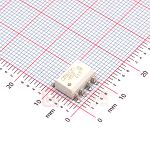
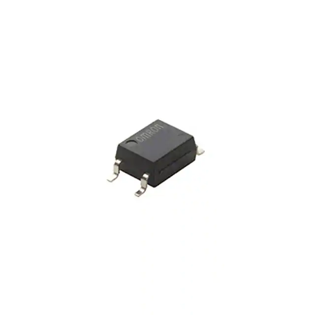
MOS FET Relays
G3VM-41GR8
Low 100-mΩ ON Resistance. High-power, 1-A Switching with SOP Package.
• Continuous load current of 1 A. • ON resistance of 0.1 Ω (typical) suppresses output signal attenuation. • Dielectric strength of 1,500 Vrms between I/O. • RoHS compliant
■ Application Examples
• Broadband systems • Measurement devices and Data loggers • Amusement machines
Note: The actual product is marked differently from the image shown here.
■ List of Models
Contact form SPST-NO Terminals Surface-mounting terminals Load voltage (peak value) 40 VAC Model G3VM-41GR8 Number per stick 100 Number per tape --2,500
G3VM-41GR8(TR) ---
■ Dimensions
Note: All units are in millimeters unless otherwise indicated. G3VM-41GR8
4.4±0.25
3.9±0.2
2.1 max. 0.15
Note: The actual product is marked differently from the image shown here.
0.4±0.1 2.54±0.25
0.1±0.1
0.6±0.3 7.0±0.4
Weight: 0.1 g
■ Terminal Arrangement/Internal Connections (Top View)
G3VM-41GR8
4 3
1
2
■ Actual Mounting Pad Dimensions (Recommended Value, Top View)
G3VM-41GR8
6 to 6.3 1.2
0.8 2.54
MOS FET Relays
G3VM-41GR8
117
�■ Absolute Maximum Ratings (Ta = 25°C)
Item Input LED forward current LED forward current reduction rate LED reverse voltage Connection temperature Output Load voltage (AC peak/DC) Continuous load current ON current reduction rate Connection temperature Symbol IF Δ IF/°C VR Tj VOFF IO Δ IO/°C Tj 30 −0.3 5 125 40 1,000 −13.3 125 1,500 −40 to +85 Rating Unit mA mA/°C V °C V mA mA/°C °C Vrms °C AC for 1 min With no icing or condensation With no icing or condensation 10 s Ta ≥ 50°C Ta ≥ 25°C Measurement Conditions Note: 1. The dielectric strength between the input and output was checked by applying voltage between all pins as a group on the LED side and all pins as a group on the light-receiving side.
Dielectric strength between input and VI-O output (See note 1.) Operating temperature Storage temperature Soldering temperature (10 s) Ta Tstg ---
−55 to +125 °C 260 °C
■ Electrical Characteristics (Ta = 25°C)
Item Input LED forward voltage Reverse current Capacity between terminals Trigger LED forward current Output Maximum resistance with output ON Symbol VF IR CT IFT RON Minimum 1.18 --------------1,000 ----Typical 1.33 --70 1.0 0.1 0.2 300 0.8 --1.2 0.2 Maximum 1.48 10 --3 0.13 1 500 ----3.0 0.5 Unit V μA pF mA Ω nA pF pF MΩ ms ms Measurement conditions IF = 10 mA VR = 5 V V = 0, f = 1 MHz IO = 100 mA IF = 5 mA, IO = 1 A VOFF = 30 V V = 0, f = 1MHz f = 1 MHz, Vs = 0 V VI-O = 500 VDC, RoH ≤ 60% IF = 5 mA, RL = 200 Ω, VDD = 20 V (See note 2.)
IF
Note:
2. Turn-ON and Turn-OFF Times
IF 1 2 4 3 RL VDD VOUT
Current leakage when the relay is open ILEAK Capacity between terminals Capacity between I/O terminals Insulation resistance between I/O terminals Turn-ON time Turn-OFF time COFF CI-O RI-O tON tOFF
VOUT
10% t ON
90% t OFF
■ Recommended Operating Conditions
Use the G3VM under the following conditions so that the Relay will operate properly.
Item Load voltage (AC peak/DC) Operating LED forward current Symbol VDD IF Minimum --5 --25 --10 ----Typical Maximum 32 20 1,000 60 V mA mA °C Unit
Continuous load current (AC peak/DC) IO Operating temperature Ta
118
MOS FET Relays
G3VM-41GR8
�■ Engineering Data
LED forward current vs. Ambient temperature
IF - Ta
LED forward current IF (mA) Continuous load current I O (A)
50
1.2
Continuous load current vs. Ambient temperature
IO - Ta
LED forward current I F (mA)
100 50 30
LED forward current vs. LED forward voltage
IF - VF
Ta=25
40
1
0.8
30
0.6
10 5 3
20
0.4
10
0.2
0 -20
0
20
40
60
80
100
120
0 -20
0
20
40
60
80
100
120
1
1
1.1
1.2
1.3
1.4
1.5
1.6
Ambient temperature Ta (
)
Ambient temperature Ta
LED forward voltage VF (V)
Continuous load current vs. On-state voltage
IO - VON
Continuous load current IO (A)
Ta = 25 I F = 5 mA 1
On-state resistance vs. Ambient temperature
RON - Ta
Trigger LED forward current I F T (mA) On-state resistance RON (Ω)
0.2 I O == 1A 1A I F = 5 mA, tt < 1s mA, < 1s
2
Trigger LED forward current vs. Ambient temperature
IFT - Ta
IO == 100 mA 100 mA t
很抱歉,暂时无法提供与“G3VM-41GR8TR”相匹配的价格&库存,您可以联系我们找货
免费人工找货- 国内价格
- 1+4.41931
- 30+4.26692
- 100+3.96214
- 500+3.65736
- 1000+3.50497
- 国内价格
- 1+7.0785
- 10+5.94
- 600+3.8808
- 国内价格
- 1+7.81001
- 30+7.53501
- 100+6.98501
- 500+6.435
- 1000+6.16
- 国内价格
- 1+5.78
- 10+4.99
- 50+4.36
- 100+4.01
- 500+3.61
- 1000+3.33