ON Semiconductort NPN
Complementary Silicon Plastic Power Darlingtons
. . . for use as output devices in complementary general purpose amplifier applications.
BDV65B
PNP
BDV64B
DARLINGTONS 10 AMPERES COMPLEMENTARY SILICON POWER TRANSISTORS 60 − 80 − 100 − 120 VOLTS 125 WATTS
• High DC Current Gain • w
HFE = 1000 (min.) @ 5 Adc Monolithic Construction with Built−in Base Emitter Shunt Resistors
These devices are available in Pb−free package(s). Specifications herein apply to both standard and Pb−free devices. Please see our website at www.onsemi.com for specific Pb−free orderable part numbers, or contact your local ON Semiconductor sales office or representative.
DERATING FACTOR
ÎÎÎ Î Î Î ÎÎÎÎÎÎÎÎÎÎÎÎÎÎÎÎÎÎÎÎÎÎÎ ÎÎÎÎÎÎÎÎÎÎÎÎÎÎÎÎÎÎÎÎÎ Î Î ÎÎÎÎÎÎÎÎÎÎÎÎÎÎÎÎÎÎÎÎÎÎÎ Î Î Î Î Î Î Î Î Î Î Î Î Î Î Î ÎÎÎÎÎÎÎÎÎÎÎ Î ÎÎÎÎÎÎÎÎÎÎÎÎÎÎÎÎÎÎÎÎÎÎÎ Î Î ÎÎÎ Î Î Î ÎÎÎÎÎÎÎÎÎÎÎÎÎÎÎÎÎÎÎÎÎÎÎ Î Î Î ÎÎÎÎÎÎÎÎÎÎÎÎÎÎÎÎÎÎÎÎÎÎÎ Î Î Î ÎÎÎÎÎÎÎÎÎÎÎÎÎÎÎÎÎÎÎÎÎÎÎ ÎÎÎÎÎÎÎÎÎÎÎÎÎÎÎÎÎÎÎÎÎ Î ÎÎÎÎÎÎÎÎ Î Î Î ÎÎÎÎÎÎÎÎÎÎÎÎÎÎÎÎ ÎÎÎ Î Î Î ÎÎÎÎÎÎÎÎÎÎÎÎÎÎÎÎÎÎÎÎÎÎÎ Î Î Î ÎÎÎÎÎÎÎÎÎÎÎÎÎÎÎÎÎÎÎÎÎÎÎ ÎÎÎÎÎÎÎÎÎÎÎÎÎÎÎÎÎÎÎÎ ÎÎÎÎÎÎÎÎÎÎÎÎÎÎÎÎÎÎÎÎÎÎÎ Î Î ÎÎÎÎÎÎÎÎ Î Î Î Î Î Î ÎÎÎÎÎÎÎÎÎÎÎÎÎÎÎÎ ÎÎÎ Î Î Î ÎÎÎÎÎÎÎÎÎÎÎÎÎÎÎÎÎÎÎÎÎÎÎ ÎÎÎÎÎÎÎÎÎÎÎÎÎÎÎÎÎÎÎÎ Î Î ÎÎÎÎÎÎÎÎÎÎÎÎÎÎÎÎÎÎÎÎÎÎÎ Î ÎÎÎÎÎÎÎÎÎÎÎÎÎÎÎÎÎÎÎÎÎÎÎ Î Î Î ÎÎÎÎÎÎÎÎÎÎÎÎÎÎÎÎÎÎÎÎÎÎÎ Î Î Î ÎÎÎÎÎÎÎÎÎÎÎÎÎÎÎÎÎÎÎÎÎÎÎ Î Î Î ÎÎÎÎÎÎÎÎÎÎÎÎÎÎÎÎÎÎÎÎÎÎÎ Î Î Î ÎÎÎÎÎÎÎÎÎÎÎÎÎÎÎÎÎÎÎÎÎÎÎ Î Î Î ÎÎÎÎÎÎÎÎÎÎÎÎÎÎÎÎÎÎÎÎÎÎÎ Î Î Î Î Î Î Î Î Î Î Î Î Î Î Î ÎÎÎÎÎÎÎÎÎÎÎ Î ÎÎÎÎÎÎÎÎÎÎÎÎÎÎÎÎÎÎÎÎÎÎÎ Î Î ÎÎÎÎÎÎÎÎÎÎÎÎÎÎÎÎÎÎÎÎÎÎÎ
MAXIMUM RATINGS
Rating Symbol VCEO VCB VEB IC IB Value 100 100 5.0 10 20 Unit Vdc Vdc Vdc Adc Adc Collector−Emitter Voltage Collector−Base Voltage Emitter−Base Voltage Collector Current — Continuous — Peak Base Current 0.5 Total Device Dissipation @ TC = 25_C Derate above 25_C PD 125 1.0 Watts W/_C _C Operating and Storage Junction Temperature Range TJ, Tstg – 65 to + 150
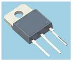
CASE 340D−02 SOT 93, TO−218 TYPE
THERMAL CHARACTERISTICS
Characteristic
Symbol θJC
Max 1.0
Unit
Thermal Resistance, Junction to Case
_C/W
1.0
0.8
0.6
0.4 0.2
0
0
25
50 100 75 TC, CASE TEMPERATURE (°C)
125
150
Figure 1. Power Derating
© Semiconductor Components Industries, LLC, 2006
March, 2006 − Rev. 12
1
Publication Order Number: BDV65B/D
�ÎÎÎÎÎÎÎÎÎÎÎÎÎÎÎÎÎÎÎÎÎÎÎÎÎÎÎÎÎÎÎÎÎ Î ÎÎ Î ÎÎÎÎÎÎÎÎÎÎÎÎÎÎÎÎÎÎÎÎÎÎÎÎÎÎÎÎÎÎÎÎÎ Î ÎÎ Î ÎÎÎÎÎÎÎÎÎÎÎÎÎÎÎÎÎÎÎÎÎÎÎÎÎÎÎÎÎÎÎÎÎ Î ÎÎ Î ÎÎÎÎÎÎÎÎÎÎÎÎÎÎÎÎÎÎÎÎÎÎÎÎÎÎÎÎÎÎÎÎÎ Î ÎÎ Î ÎÎÎÎÎÎÎÎÎÎÎÎÎÎÎÎÎÎÎÎÎÎÎÎÎÎÎÎÎÎÎÎÎ Î ÎÎ Î ÎÎÎÎÎÎÎÎÎÎÎÎÎÎÎÎÎÎÎÎÎÎÎÎÎÎÎÎÎÎÎÎÎ Î ÎÎ Î Î ÎÎÎÎÎÎÎÎÎÎÎÎ Î ÎÎ Î ÎÎÎÎÎÎÎÎÎÎÎÎÎÎÎÎÎÎÎÎÎÎÎÎÎÎÎÎÎÎÎÎÎ Î ÎÎÎÎÎÎÎÎÎÎÎÎÎÎÎÎÎÎÎÎ ÎÎÎ Î Î Î ÎÎ ÎÎÎÎÎÎÎÎÎÎÎÎÎÎÎÎÎÎÎÎÎÎÎÎÎÎÎÎÎÎÎÎÎ Î Î Î Î Î Î Î Î Î Î ÎÎÎÎÎÎÎÎÎÎÎÎÎÎÎÎÎÎÎÎÎ ÎÎÎÎÎÎÎÎÎÎÎÎÎÎÎÎÎÎÎÎÎÎÎÎÎÎÎÎÎÎÎÎÎ Î ÎÎÎÎÎÎÎÎÎÎÎÎÎÎÎÎÎÎÎÎÎÎÎÎÎÎÎÎÎÎÎÎÎ Î ÎÎ Î ÎÎÎ Î Î Î Î ÎÎÎÎÎÎÎÎÎÎÎÎÎÎÎÎÎÎÎÎÎÎÎÎÎÎÎÎÎÎÎÎÎ ÎÎÎÎÎÎÎÎÎÎÎÎÎÎÎÎÎÎÎÎÎÎÎÎÎÎÎÎÎÎÎ ÎÎ Î ÎÎÎÎÎÎÎÎÎÎÎÎÎÎÎÎÎÎÎÎÎÎÎÎÎÎÎÎÎÎÎÎÎ Î ÎÎ Î ÎÎÎÎÎÎÎÎÎÎÎÎÎÎÎÎÎÎÎÎÎÎÎÎÎÎÎÎÎÎÎÎÎ Î ÎÎ Î ÎÎÎ Î Î Î Î ÎÎÎÎÎÎÎÎÎÎÎÎÎÎÎÎÎÎÎÎÎÎÎÎÎÎÎÎÎÎÎÎÎ Î ÎÎ Î ÎÎÎÎÎÎÎÎÎÎÎÎÎÎÎÎÎÎÎÎÎÎÎÎÎÎÎÎÎÎÎÎÎ Î ÎÎ Î ÎÎÎÎÎÎÎÎÎÎÎÎÎÎÎÎÎÎÎÎÎÎÎÎÎÎÎÎÎÎÎÎÎ ÎÎÎÎÎÎÎÎÎÎÎÎÎÎÎÎÎÎÎÎÎÎÎÎÎÎÎÎÎÎÎ Î ÎÎÎÎÎÎÎÎÎÎÎÎ Î ÎÎ ÎÎ Î Î ÎÎÎÎÎÎÎÎÎÎÎÎÎÎÎÎÎÎÎÎÎÎ ÎÎ ÎÎ Î ÎÎÎÎÎÎÎÎÎÎÎÎÎÎÎÎÎÎÎÎÎÎÎÎÎÎÎÎÎÎÎÎÎ ÎÎÎÎÎÎÎÎÎÎÎÎÎÎÎÎÎÎÎÎÎÎÎÎÎÎÎÎÎÎÎÎÎ ÎÎÎÎÎÎÎÎÎÎÎÎÎÎÎÎÎÎÎÎÎÎÎÎÎÎÎÎÎÎÎ Î ÎÎ ÎÎÎÎÎÎÎÎÎÎÎÎÎÎÎÎÎÎÎÎÎÎÎÎÎÎÎÎÎÎÎÎÎ Î ÎÎ ÎÎÎÎÎÎÎÎÎÎÎÎÎÎÎÎÎÎÎÎÎÎÎÎÎÎÎÎÎÎÎÎÎ Î ÎÎÎÎÎÎÎÎÎÎÎÎÎÎÎÎÎÎÎÎÎÎÎÎÎÎÎÎÎÎÎÎÎ Î ÎÎÎÎÎÎÎÎÎÎÎÎÎÎÎÎÎÎÎÎÎÎÎÎÎÎÎÎÎÎÎÎÎ Î ÎÎ ÎÎÎÎÎÎÎÎÎÎÎÎÎÎÎÎÎÎÎÎÎÎÎÎÎÎÎÎÎÎÎÎÎ
ELECTRICAL CHARACTERISTICS
ON CHARACTERISTICS OFF CHARACTERISTICS Base−Emitter Saturation Voltage (IC = 5.0 Adc, VCE = 4.0 Vdc) Collector−Emitter Saturation Voltage (IC = 5.0 Adc, IB = 0.02 Adc) DC Current Gain (IC = 5.0 Adc, VCE = 4.0 Vdc) Emitter Cutoff Current (VBE = 5.0 Vdc, IC = 0) Collector Cutoff Current (VCB = 50 Vdc, IE = 0, TC = 150_C) Collector Cutoff Current (VCB = 100 Vdc, IE = 0) Collector Cutoff Current (VCE = 50 Vdc, IB = 0) Collector−Emitter Sustaining Voltage (1) (IC = 30 mAdc, IB = 0) Characteristic
NPN
VCE = 4 V
hFE , DC CURRENT GAIN
hFE , DC CURRENT GAIN
10K
1K
4
0.1
Figure 2. DC Current Gain
1 IC, COLLECTOR CURRENT (A)
BDV65B BDV64B
http://onsemi.com
10 10K 1K 1 0.1
2
PNP
Figure 3. DC Current Gain
VCEO(sus) Symbol VCE(sat) 1 IC, COLLECTOR CURRENT (A) VBE(on) ICBO ICBO ICEO IEBO hFE 1000 Min 100 — — — — — — Max 2.5 2.0 5.0 2.0 0.4 1.0 — — — mAdc mAdc mAdc mAdc Unit Vdc Vdc Vdc 10
�BDV65B BDV64B
10 10
V, VOLTAGE (V)
1
VBE(sat) @ IC/IB = 250
V, VOLTAGE (V)
1
VBE(sat) @ IC/IB = 250
0.1
0.1
1 IC, COLLECTOR CURRENT (A)
10
0.1
0.1
1 IC, COLLECTOR CURRENT (A)
10
Figure 4. “On” Voltages
Figure 5. “On” Voltages
100 50 IC, COLLECTOR CURRENT (A) 20 dc SECONDARY BREAKDOWN LIMITED @ TJ v 150°C THERMAL LIMIT @ TC = 25°C BONDING WIRE LIMIT BDV65B, BDV64B 1 10 50 30 VCE, COLLECTOR−EMITTER VOLTAGE (V) 100 100 μs 5.0 ms 1.0 ms
10 5
1
There are two limitations on the power handling ability of a transistor: average junction temperature and second breakdown. Safe operating area curves indicate IC − VCE limits of the transistor that must be observed for reliable operation i.e., the transistor must not be subjected to greater dissipation than the curves indicate. The data of Figure 6 is based on TJ(pk) = 150_C, TC is variable depending on conditions. Second breakdown pulse limits are valid for duty cycles to 10% provided TJ(pk) v 150_C. TJ(pk) may be calculated from the data in Figure 7. At high case temperatures, thermal limitations will reduce the power that can be handled to values less than the limitations imposed by second breakdown.
Figure 6. Active Region Safe Operating Area
r(t), TRANSIENT THERMAL RESISTANCE (NORMALIZED)
1.0 0.5 0.2 0.1 D = 0.5 0.2 0.1 0.05 0.02 0.01 t1 (SINGLE PULSE) 0.05 0.1 0.5 1.0 5 t, TIME (ms) P(pk) ZθJC(t) = r(t) RθJC RθJC = 1.0°C/W MAX D CURVES APPLY FOR POWER PULSE TRAIN SHOWN READ TIME AT t1 TJ(pk) − TC = P(pk) ZθJC(t) 50 100 500 1000
0.05 0.03
t2
DUTY CYCLE, D = t1/t2 10
0.01 0.01
Figure 7. Thermal Response
http://onsemi.com
3
�BDV65B BDV64B
PACKAGE DIMENSIONS CASE 340D−02 ISSUE E
C B Q E
NOTES: 1. DIMENSIONING AND TOLERANCING PER ANSI Y14.5M, 1982. 2. CONTROLLING DIMENSION: MILLIMETER. DIM A B C D E G H J K L Q S U V MILLIMETERS MIN MAX −−− 20.35 14.70 15.20 4.70 4.90 1.10 1.30 1.17 1.37 5.40 5.55 2.00 3.00 0.50 0.78 31.00 REF −−− 16.20 4.00 4.10 17.80 18.20 4.00 REF 1.75 REF BASE COLLECTOR EMITTER COLLECTOR INCHES MIN MAX −−− 0.801 0.579 0.598 0.185 0.193 0.043 0.051 0.046 0.054 0.213 0.219 0.079 0.118 0.020 0.031 1.220 REF −−− 0.638 0.158 0.161 0.701 0.717 0.157 REF 0.069
U S K L
1 2
4
A
3
D V G
J H
STYLE 1: PIN 1. 2. 3. 4.
ON Semiconductor and are registered trademarks of Semiconductor Components Industries, LLC (SCILLC). SCILLC reserves the right to make changes without further notice to any products herein. SCILLC makes no warranty, representation or guarantee regarding the suitability of its products for any particular purpose, nor does SCILLC assume any liability arising out of the application or use of any product or circuit, and specifically disclaims any and all liability, including without limitation special, consequential or incidental damages. “Typical” parameters which may be provided in SCILLC data sheets and/or specifications can and do vary in different applications and actual performance may vary over time. All operating parameters, including “Typicals” must be validated for each customer application by customer’s technical experts. SCILLC does not convey any license under its patent rights nor the rights of others. SCILLC products are not designed, intended, or authorized for use as components in systems intended for surgical implant into the body, or other applications intended to support or sustain life, or for any other application in which the failure of the SCILLC product could create a situation where personal injury or death may occur. Should Buyer purchase or use SCILLC products for any such unintended or unauthorized application, Buyer shall indemnify and hold SCILLC and its officers, employees, subsidiaries, affiliates, and distributors harmless against all claims, costs, damages, and expenses, and reasonable attorney fees arising out of, directly or indirectly, any claim of personal injury or death associated with such unintended or unauthorized use, even if such claim alleges that SCILLC was negligent regarding the design or manufacture of the part. SCILLC is an Equal Opportunity/Affirmative Action Employer. This literature is subject to all applicable copyright laws and is not for resale in any manner.
PUBLICATION ORDERING INFORMATION
LITERATURE FULFILLMENT: Literature Distribution Center for ON Semiconductor P.O. Box 61312, Phoenix, Arizona 85082−1312 USA Phone: 480−829−7710 or 800−344−3860 Toll Free USA/Canada Fax: 480−829−7709 or 800−344−3867 Toll Free USA/Canada Email: orderlit@onsemi.com N. American Technical Support: 800−282−9855 Toll Free USA/Canada Japan: ON Semiconductor, Japan Customer Focus Center 2−9−1 Kamimeguro, Meguro−ku, Tokyo, Japan 153−0051 Phone: 81−3−5773−3850 ON Semiconductor Website: http://onsemi.com Order Literature: http://www.onsemi.com/litorder For additional information, please contact your local Sales Representative.
http://onsemi.com
4
BDV65B/D
�