Is Now Part of
To learn more about ON Semiconductor, please visit our website at
www.onsemi.com
Please note: As part of the Fairchild Semiconductor integration, some of the Fairchild orderable part numbers
will need to change in order to meet ON Semiconductor’s system requirements. Since the ON Semiconductor
product management systems do not have the ability to manage part nomenclature that utilizes an underscore
(_), the underscore (_) in the Fairchild part numbers will be changed to a dash (-). This document may contain
device numbers with an underscore (_). Please check the ON Semiconductor website to verify the updated
device numbers. The most current and up-to-date ordering information can be found at www.onsemi.com. Please
email any questions regarding the system integration to Fairchild_questions@onsemi.com.
ON Semiconductor and the ON Semiconductor logo are trademarks of Semiconductor Components Industries, LLC dba ON Semiconductor or its subsidiaries in the United States and/or other countries. ON Semiconductor owns the rights to a number
of patents, trademarks, copyrights, trade secrets, and other intellectual property. A listing of ON Semiconductor’s product/patent coverage may be accessed at www.onsemi.com/site/pdf/Patent-Marking.pdf. ON Semiconductor reserves the right
to make changes without further notice to any products herein. ON Semiconductor makes no warranty, representation or guarantee regarding the suitability of its products for any particular purpose, nor does ON Semiconductor assume any liability
arising out of the application or use of any product or circuit, and specifically disclaims any and all liability, including without limitation special, consequential or incidental damages. Buyer is responsible for its products and applications using ON
Semiconductor products, including compliance with all laws, regulations and safety requirements or standards, regardless of any support or applications information provided by ON Semiconductor. “Typical” parameters which may be provided in ON
Semiconductor data sheets and/or specifications can and do vary in different applications and actual performance may vary over time. All operating parameters, including “Typicals” must be validated for each customer application by customer’s
technical experts. ON Semiconductor does not convey any license under its patent rights nor the rights of others. ON Semiconductor products are not designed, intended, or authorized for use as a critical component in life support systems or any FDA
Class 3 medical devices or medical devices with a same or similar classification in a foreign jurisdiction or any devices intended for implantation in the human body. Should Buyer purchase or use ON Semiconductor products for any such unintended
or unauthorized application, Buyer shall indemnify and hold ON Semiconductor and its officers, employees, subsidiaries, affiliates, and distributors harmless against all claims, costs, damages, and expenses, and reasonable attorney fees arising out
of, directly or indirectly, any claim of personal injury or death associated with such unintended or unauthorized use, even if such claim alleges that ON Semiconductor was negligent regarding the design or manufacture of the part. ON Semiconductor
is an Equal Opportunity/Affirmative Action Employer. This literature is subject to all applicable copyright laws and is not for resale in any manner.
�FAN23SV10MAMPX
10 A Synchronous Buck Regulator
Features
Description
VIN Range: 7 V to 18 V Using Internal Linear
Regulator for Bias
VIN Range: 4.5 V to 5.5 V with VIN/PVIN/PVCC
Connected to Bypass Internal Regulator
High Efficiency: Over 96% Peak
The FAN23SV10MA is a highly efficient synchronous
buck regulator. The regulator is capable of operating
with an input range from 7 V to 18 V and supporting up
to 10 A load currents. The device can operate from a
5 V rail (±10%) if VIN, PVIN, and PVCC are connected
together to bypass the internal linear regulator.
Continuous Output Current: 10 A
Internal Linear Bias Regulator
Accurate Enable facilitates VIN UVLO Functionality
PFM Mode for Light-Load Efficiency
Excellent Line and Load Transient Response
Precision Reference: ±1% Over Temperature
Output Voltage Range: 0.6 to 5.5 V
Programmable Frequency: 200 kHz to 1.5 MHz
Programmable Soft-Start
Low Shutdown Current
Adjustable Sourcing Current Limit
This FAN23SV10MA utilizes Fairchild’s constant ontime control architecture to provide excellent transient
response and to maintain a relatively constant switching
frequency. The device utilizes Pulse Frequency
Modulation (PFM) mode to maximize light-load
efficiency by reducing switching frequency when the
inductor is operating in discontinuous conduction mode
at light loads.
Switching frequency and over-current protection can
be programmed to provide a flexible solution for
various applications. Output over-voltage, undervoltage, over-current, and thermal shutdown protections
help prevent damage to the device during fault
conditions. After thermal shutdown is activated, a
hysteresis feature restarts the device when normal
operating temperature is reached.
Internal Boot Diode
Thermal Shutdown
Halogen and Lead Free, RoHS Compliant
Applications
Servers and Desktop Computers
NVDC Notebooks, Netbooks
Game Consoles
Telecommunications
Storage
Ordering Information
Part Number
Configuration
Operating
Temperature Range
Output
Current (A)
Package
FAN23SV10MAMPX
PFM, No Ultrasonic Mode
-40 to 125°C
10
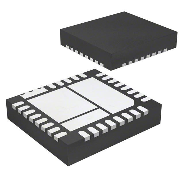
34-Lead, PQFN,
5.5 mm x 5.0 mm
© 2015 Fairchild Semiconductor Corporation
FAN23SV10MA . • Rev. 1.0
www.fairchildsemi.com
FAN23SV10MAMPX — 10 A Synchronous Buck Regulator
September 2015
�VIN = 12V
VIN = 12V
R11
10Ω
C9
0.1µF
C10
2.2µF
CIN
0.1µF
R7
64.9kΩ
PVCC
VCC
Ext
EN
VIN
PVIN
C3
0.1µF
EN
R7, R8 used for Accurate EN
R7, R8 open for Ext EN
CIN
3x10µF
R8
10kΩ
L1
0.72µH
SW
PGOOD
ILIM
SOFT START
R2
1.5kΩ
R5 1.58kΩ
C7
15nF
VOUT = 1.2V
IOUT=0-10A
BOOT
FAN23SV10MA
C4
0.1µF
C5
100pF
FREQ
R3
10kΩ
COUT
6x47µF
FB
R9
54.9kΩ
AGND
R6
4.99kΩ
PGND
R4
10kΩ
Figure 1. Typical Application with VIN=12 V
VIN = 5V
R11
10Ω
C9
0.1µF
PVCC
VCC
Ext
EN
C10
2.2µF
CIN
0.1µF
VIN
CIN
3x10µF
PVIN
C3
0.1µF
EN
FAN23SV10MA
L1
0.72µH
ILIM
SOFT START
R5 1.58kΩ
R2
1.5kΩ
C4
0.1µF
C5
100pF
FREQ
R9
54.9kΩ
VOUT = 1.2V
IOUT=0-10A
BOOT
SW
PGOOD
C7
15nF
FAN23SV10MAMPX — 10 A Synchronous Buck Regulator
Typical Application Diagram
R3
10kΩ
COUT
6x47µF
FB
AGND
R6
4.99kΩ
PGND
R4
10kΩ
Figure 2. Typical Application with VIN=5 V
© 2015 Fairchild Semiconductor Corporation
FAN23SV10M • Rev. 1.12
www.fairchildsemi.com
2
�FAN23SV10MAMPX — 10 A Synchronous Buck Regulator
Functional Block Diagram
VIN
BOOT
PVIN
PVCC
Linear
Regulator
PVCC
VCC
VCC
VCC UVLO
1.26V/1.14V
PVCC
EN
ENABLE
VCC
VCC
10µA
Modulator
HS Gate
Driver
SS
FB
VREF
FB
Comparator
SW
FREQ
PFM
Comparator
Control
Logic
x1.2
2nd Level OVP
Comparator
x1.1
1st Level OVP
Comparator
x0.9
Under-Voltage
Comparator
PVCC
LS Gate
Driver
VCC
PGOOD
Thermal
Shutdown
10µA
Current Limit
Comparator
AGND
ILIM
PGND
Figure 3. Block Diagram
© 2015 Fairchild Semiconductor Corporation
FAN23SV10MA • Rev. 1.0
www.fairchildsemi.com
3
�9
VIN
PVIN
9
SW
PVIN
8
BOOT
PVIN
7
AGND
PVIN
6
PVIN
PVIN
5
PVIN
AGND
4
PVIN
BOOT
3
PVIN
SW
2
PVIN
VIN
1
8
7
6
5
4
3
2
1
10
PVIN
PVIN 10
34
NC
11
PVIN
PVIN 11
33
NC
12
SW
SW
12
32
FREQ
13
SW
SW 13
31
SS
14
SW
SW
30 PGOOD
29
15
SW
SW 15
29
EN
NC
28
16
SW
SW 16
28
NC
FB
27
17
SW
SW 17
27
FB
24
23
22
21
20
PVCC
ILIM
AGND
SW
PGND
PGND
19
18
Figure 4. Pin Assignments, Bottom View
18
19
20
21
22
23
24
25
26
VCC
26
25
VCC
EN
14
PVCC
SW
(P3)
PGOOD 30
ILIM
AGND
(P1)
AGND
31
SW
SS
PGND
32
PGND
FREQ
PGND
33
PGND
NC
PVIN
(P2)
PGND
34
PGND
NC
Figure 5. Pin Assignments, Top View
Pin Definitions
Name
Pad / Pin
PVIN
P2, 5-11
VIN
1
Power input to the linear regulator; used in the modulator for input voltage feed-forward
PVCC
25
Power output of the linear regulator; directly supplies power for the low-side gate driver
and boot diode. Can be connected to VIN and PVIN for operation from 5 V rail.
VCC
26
Power supply input for the controller
PGND
18-21
AGND
P1, 4, 23
SW
Description
Power input for the power stage
Power ground for the low-side power MOSFET and for the low-side gate driver
Analog ground for the analog portions of the IC and for substrate
P3, 2, 12-17, 22 Switching node; junction between high-and low-side MOSFETs
BOOT
3
Supply for high-side MOSFET gate driver. A capacitor from BOOT to SW supplies the
charge to turn on the N-channel high-side MOSFET. During the freewheeling interval
(low-side MOSFET on), the high-side capacitor is recharged by an internal diode
connected to PVCC.
ILIM
24
Current limit. A resistor between ILIM and SW sets the current limit threshold.
FB
27
Output voltage feedback to the modulator
EN
29
Enable input to the IC. Pin must be driven logic high to enable, or logic low to disable.
SS
31
Soft-start input to the modulator
FREQ
32
On-time and frequency programming pin. Connect a resistor between FREQ and
AGND to program on-time and switching frequency.
PGOOD
30
Power good; open-drain output indicating VOUT is within set limits.
NC
28, 33-34
Leave pin open or connect to AGND.
© 2015 Fairchild Semiconductor Corporation
FAN23SV10MA • Rev. 1.0
www.fairchildsemi.com
4
FAN23SV10MAMPX — 10 A Synchronous Buck Regulator
Pin Configuration
�Stresses exceeding the absolute maximum ratings may damage the device. The device may not function or be
operable above the recommended operating conditions and stressing the parts to these levels is not recommended.
In addition, extended exposure to stresses above the recommended operating conditions may affect device reliability.
The absolute maximum ratings are stress ratings only.
Symbol
VPVIN
VIN
VBOOT
VSW
Parameter
Conditions
Min. Max. Unit
Power Input
Referenced to PGND
-0.3
25.0
V
Modulator Input
Referenced to AGND
-0.3
25.0
V
Referenced to PVCC
-0.3
26.0
V
Referenced to PVCC, +11% of VREF (666 mV), both HS and LS
turn off. By turning off the LS during an OV event, V OUT
overshoot can be reduced when there is positive
inductor current by increasing the rate of discharge.
Once the VFB voltage falls below VREF, the latched OV
signal is cleared and operation returns to normal.
�The inductor is typically selected based on the ripple
current (IL), which is approximately 25% to 45% of the
maximum DC load. The inductor current rating should
be selected such that the saturation and heating current
ratings exceed the intended currents encountered in the
application over the expected temperature range of
operation. Regulators that require fast transient
response use smaller inductance and higher current
ripple; while regulators that require higher efficiency
keep ripple current on the low side.
The inductor value is given by:
(21)
where IMAX and IMIN are maximum and minimum
load steps, respectively and VOUT is the voltage
overshoot, usually specified from 3 to 5%.
For example: for VI=12 V, VOUT=1.2 V, 6 A IMAX, 2 A IMIN,
fSW=500 kHz, LOUT=720 nH, and 3% VOUT deviation of
36 mV; the COUT value is calculated to be 263 µF. This
capacitor requirement can be satisfied using six 47 µF,
6.3 V-rated X5R ceramic capacitors. This calculation
applies for load current slew rates that are faster than
the inductor current slew rate, which can be defined as
VOUT/L during the load current removal. For reducedload-current slew rates and/or reduced transient
requirements, the output capacitor value may be
reduced and comprised of low-cost 22 µF capacitors.
(18)
For example: for 12 V VIN, 1.2 V VOUT, 10 A load, 30%
IL, and 500 kHz fSW; L is 720 nH, and a standard value
of 680 nH is selected.
Input Capacitor Selection
Input capacitor CIN is selected based on voltage rating,
RMS current ICIN(RMS) rating, and capacitance. For
capacitors having DC voltage bias derating, such as
ceramic capacitors, higher rating is strongly
recommended. RMS current rating is given by:
Setting the Current Limit
Current limit is implemented by sensing the inductor
valley current across the LS MOSFET VDS during the LS
on-time. The current limit comparator prevents a new
on-time from being started until the valley current is less
than the current limit.
(19)
where ILOAD-MAX is the maximum load current and D is
the duty cycle VOUT/VIN. The maximum ICIN(RMS) occurs
at 50% duty cycle.
The capacitance is given by:
The set point is configured by connecting a resistor from
the ILIM pin to the SW pin. A trimmed current is output
onto the ILIM pin, which creates a voltage across the
resistor. When the voltage on ILIM goes negative, an
over-current condition is detected.
(20)
RILIM is calculated by:
where VIN is the input voltage ripple, normally 1% of
VIN.
(22)
where KILIM is the current source scale factor, and
IVALLEY is the inductor valley current when the current
limit threshold is reached. The factor 1.04 accounts
for the temperature offset of the LS MOSFET
compared to the control circuit.
With the constant on-time architecture, HS is always
turned on for a fixed on-time; this determines the peakto-peak inductor current.
For example; for VIN=12 V, VIN=120 mV, VOUT=1.2 V,
10 A load, and fSW=500 kHz; CIN is 15 µF and ICIN(RMS) is
3 ARMS. Select two 10 µF 25 V-rated ceramic capacitors
with X7R or similar dielectric, recognizing that the
capacitor DC bias characteristic indicates that the
capacitance value falls approximately 40% at V IN=12 V,
with a resultant small increase in VIN ripple voltage
above 120 mV used in the calculation. Also, each 10 µF
can carry over 3 ARMS in the frequency range from
100 kHz to 1 MHz, exceeding the input capacitor current
rating requirements. An additional 1 µF capacitor may
be needed to suppress noise generated by high
frequency switching transitions.
Current ripple I is given by:
(23)
From the equation above, the worst-case ripple occurs
during an output short circuit (where VOUT is 0 V). This
should be taken into account when selecting the current
limit set point.
Output Capacitor Selection
Output capacitor COUT is also selected based on voltage
rating, RMS current ICIN (RMS) rating, and
capacitance. For capacitors having DC voltage bias
derating, such as ceramic capacitors, higher rating is
highly recommended.
When calculating COUT, usually the dominant
requirement is the current load step transient. If the
unloading transient requirement (IOUT transitioning from
HIGH to LOW), is satisfied, then the load transient (IOUT
transitioning LOW to HIGH), is also usually satisfied.
© 2015 Fairchild Semiconductor Corporation
FAN23SV10MA • Rev. 1.0
www.fairchildsemi.com
14
FAN23SV10MAMPX — 10 A Synchronous Buck Regulator
The unloading COUT calculation, assuming COUT has
negligible parasitic resistance and inductance in the
circuit path, is given by:
Inductor Selection
�Power circuit loops that carry high currents should be
arranged to minimize the loop area. Primary focus
should be directed to minimize the loop for current flow
from the input capacitor to PVIN, through the internal
MOSFETs, and returning to the input capacitor. The
input capacitor should be placed as close to the PVIN
terminals as possible.
The valley current level for calculating RILIM is given by:
(24)
where ILOAD(CL) is the DC load current when the
current limit threshold is reached.
The current return path from PGND at the low-side
MOSFET source to the negative terminal of the input
capacitor can be routed under the inductor and also
through vias that connect the input capacitor and lowside MOSFET source to the PGND region under the
power portion of the IC.
For example: In a converter designed for 10 A steadystate operation and 3 A current ripple, the current-limit
threshold could be selected at 120% of ILOAD,(SS) to
accommodate transient operation and inductor value
decrease under loading. As a result, ILOAD,(CL) is 12 A,
IVALLEY=10.5 A, and RILIM is selected as the standard
value of 1.58kΩ.
The SW node trace which connects the source of the
high-side MOSFET and the drain of the low-side
MOSFET to the inductor should be short and wide.
Boot Resistor
To control the voltage across the output capacitor, the
output voltage divider should be located close to the FB
pin, with the upper FB voltage divider resistor connected
to the positive side of the output capacitor, and the
bottom resistor should be connected to the AGND
portion of the FAN23SV10MA device.
In some applications, especially with higher input voltage,
the VSW ring voltage may exceed derating guidelines of
80% to 90% of absolute rating for VSW. In this situation a
resistor can be connected in series with boot capacitor
(C3 in Figure 1) to reduce the turn-on speed of the high
side MOSFET to reduce the amplitude of the VSW ring
voltage.
When using ceramic capacitor solutions with external
ramp injection circuitry (R2, C4, C5 in Figure 1), R2 and
C4 should be connected near the inductor, and coupling
capacitor C5 should be placed near FB pin to minimize
FB pin trace length.
Printed Circuit Board (PCB) Layout
Guidelines
The following points should be considered before
beginning a PCB layout using the FAN23SV10MA. A
sample PCB layout from the evaluation board is shown
in Figure 24-Figure 27 following the layout guidelines.
Decoupling capacitors for PVCC and VCC should be
located close to their respective device pins.
SW node connections to BOOT, ILIM, and ripple injection
resistor R2 should be made through separate traces.
Power components consisting of the input capacitors,
output capacitors, inductor, and FAN23SV10MA device
should be placed on a common side of the pcb in close
proximity to each other and connected using surface
copper.
Sensitive analog components including SS, FB, ILIM,
FREQ, and EN should be placed away from the highvoltage switching circuits such as SW and BOOT, and
connected to their respective pins with short traces.
The inner PCB layer closest to the FAN23SV10MA
device should have Power Ground (PGND) under the
power processing portion of the device (PVIN, SW, and
PGND). This inner PCB layer should have a separate
Analog Ground (AGND) under the P1 pad and the
associated analog components. AGND and PGND
should be connected together near the IC between
PGND pins 18-21 and AGND pin 23 which connects to
P1 thermal pad.
The AGND thermal pad (P1) should be connected to
AGND plane on inner layer using four 0.25 mm vias
spread under the pad. No vias are included under PVIN
(P2) and SW (P3) to maintain the PGND plane under
the power circuitry intact.
© 2015 Fairchild Semiconductor Corporation
FAN23SV10MA • Rev. 1.0
www.fairchildsemi.com
15
FAN23SV10MAMPX — 10 A Synchronous Buck Regulator
The FAN23SV10MA uses valley-current sensing; the
current limit (IILIM) set point is the valley (IVALLEY).
�FAN23SV10MAMPX — 10 A Synchronous Buck Regulator
Figure 24. Evaluation Board Top Layer Copper
Figure 25. Evaluation Board Inner Layer 1 Copper
© 2015 Fairchild Semiconductor Corporation
FAN23SV10MA • Rev. 1.0
www.fairchildsemi.com
16
�FAN23SV10MAMPX — 10 A Synchronous Buck Regulator
Figure 26. Evaluation Board Inner Layer 2 Copper
Figure 27. Evaluation Board Bottom Layer Copper
© 2015 Fairchild Semiconductor Corporation
FAN23SV10MA • Rev. 1.0
www.fairchildsemi.com
17
�5.50±0.10
26
18
1.05±0.10
17
27
0.25±0.05 (30X)
5.00±0.10
34
0.25±0.05
0.025±0.025
10
1
9
SEATING
PLANE
PIN#1
INDICATOR
SEE
DETAIL 'A'
1.58±0.01
(0.35)
SCALE: 2:1
2.18±0.01
(0.43)
0.50±0.01
9
1
(0.25)
0.40±0.01 (30X)
(0.35) 34
10
0.68±0.01
(0.35)
3.50±0.01
2.58±0.01
(1.75)
17
(0.75)
(0.33)
(0.35)
27
0.43±0.01
18
26
(0.35)
NOTES: UNLESS OTHERWISE SPECIFIED
A) NO INDUSTRY REGISTRATION APPLIES.
B) ALL DIMENSIONS ARE IN MILLIMETERS.
C) DIMENSIONS DO NOT INCLUDE BURRS
OR MOLD FLASH. MOLD FLASH OR
BURRS DOES NOT EXCEED 0.10MM.
D) DIMENSIONING AND TOLERANCING PER
ASME Y14.5M-2009.
E) DRAWING FILE NAME: MKT-PQFN34AREV2
F) FAIRCHILD SEMICONDUCTOR
(0.25)
(0.28) (3X)
(0.24)
1.75±0.01
�5.70
2.18
1.58
0.55 (30X)
2.10
(0.35)
1.80
26
18
0.55
17
27
(1.75)
2.58
4.10
3.50
3.60
(1.85)
0.68
34
10
0.75
1
(0.30)
9
(0.35)
0.50±0.05
0.43
(0.08)
4.10
LAND PATTERN
RECOMMENDATION
0.20
0.30 (30X)
5.20
�ON Semiconductor and
are trademarks of Semiconductor Components Industries, LLC dba ON Semiconductor or its subsidiaries in the United States and/or other countries.
ON Semiconductor owns the rights to a number of patents, trademarks, copyrights, trade secrets, and other intellectual property. A listing of ON Semiconductor’s product/patent
coverage may be accessed at www.onsemi.com/site/pdf/Patent−Marking.pdf. ON Semiconductor reserves the right to make changes without further notice to any products herein.
ON Semiconductor makes no warranty, representation or guarantee regarding the suitability of its products for any particular purpose, nor does ON Semiconductor assume any liability
arising out of the application or use of any product or circuit, and specifically disclaims any and all liability, including without limitation special, consequential or incidental damages.
Buyer is responsible for its products and applications using ON Semiconductor products, including compliance with all laws, regulations and safety requirements or standards,
regardless of any support or applications information provided by ON Semiconductor. “Typical” parameters which may be provided in ON Semiconductor data sheets and/or
specifications can and do vary in different applications and actual performance may vary over time. All operating parameters, including “Typicals” must be validated for each customer
application by customer’s technical experts. ON Semiconductor does not convey any license under its patent rights nor the rights of others. ON Semiconductor products are not
designed, intended, or authorized for use as a critical component in life support systems or any FDA Class 3 medical devices or medical devices with a same or similar classification
in a foreign jurisdiction or any devices intended for implantation in the human body. Should Buyer purchase or use ON Semiconductor products for any such unintended or unauthorized
application, Buyer shall indemnify and hold ON Semiconductor and its officers, employees, subsidiaries, affiliates, and distributors harmless against all claims, costs, damages, and
expenses, and reasonable attorney fees arising out of, directly or indirectly, any claim of personal injury or death associated with such unintended or unauthorized use, even if such
claim alleges that ON Semiconductor was negligent regarding the design or manufacture of the part. ON Semiconductor is an Equal Opportunity/Affirmative Action Employer. This
literature is subject to all applicable copyright laws and is not for resale in any manner.
PUBLICATION ORDERING INFORMATION
LITERATURE FULFILLMENT:
Literature Distribution Center for ON Semiconductor
19521 E. 32nd Pkwy, Aurora, Colorado 80011 USA
Phone: 303−675−2175 or 800−344−3860 Toll Free USA/Canada
Fax: 303−675−2176 or 800−344−3867 Toll Free USA/Canada
Email: orderlit@onsemi.com
© Semiconductor Components Industries, LLC
N. American Technical Support: 800−282−9855 Toll Free
USA/Canada
Europe, Middle East and Africa Technical Support:
Phone: 421 33 790 2910
Japan Customer Focus Center
Phone: 81−3−5817−1050
www.onsemi.com
1
ON Semiconductor Website: www.onsemi.com
Order Literature: http://www.onsemi.com/orderlit
For additional information, please contact your local
Sales Representative
www.onsemi.com
�