FAN48610
Fixed-Output Synchronous
Regulator, TINYBOOST),
2.5 MHz
Description
www.onsemi.com
The FAN48610 is a low-power boost regulator designed to provide
a minimum voltage-regulated rail from a standard single-cell Li-Ion
battery and advanced battery chemistries. Even below the minimum
system battery voltage, the device maintains the output voltage
regulation for a minimum output load current of 1.0 A. The
combination of built-in power transistors, synchronous rectification,
and low supply current suit the FAN48610 for battery-powered
applications.
The FAN48610 is available in a 9-bump, 0.4 mm pitch, Wafer-Level
Chip-Scale Package (WLCSP).
WLCSP9
CASE 567QW
MARKING DIAGRAM
Features
•
•
•
•
•
•
•
•
•
•
•
XX&K
&.&2&Z
Input Voltage Range: 2.5 V to 4.8 V
Output Voltages Range: 3.0 V to 5.0 V
IOUT ≥ 1 A at VOUT = 5.0 V, VIN ≥ 2.5 V
IOUT ≥ 1.5 A at VOUT = 5.0 V, VIN ≥ 3.0 V
Up to 94% Efficient
Internal Synchronous Rectification
Soft-Start with True Load Disconnect
Short-Circuit Protection
9-Bump, 1.215 mm × 1.215 mm, 0.4 mm Pitch WLCSP
Three External Components: 2016 0.47 mH Inductor,
0603 Case Size Input / Output Capacitors
Total Application Board Solution Size: < 11 mm2
XX
&K
&.
&2
&Z
= KA / KF / KN
= Lot Code
= Alphabetical Year Code
= Numeric Date Code
= Assembly Plant Code
PIN ASSIGNMENT
VOUT
A1
VIN
A2
SW
Applications
• Class-D Audio Amplifier and USB OTG Supply
• Boost for Low-Voltage Li-Ion Batteries
• Smart Phones, Tablets, Portable Devices, Wearables
B1
EN
B2
PGND
C1
A3
B3
AGND
C2
C3
(Top View)
VIN
+
CIN
COUT
10 mF
L1
Battery
VOUT
FAN48610
0.47 mH
22 mF
SW
PGND
EN
AGND
SYSTEM
LOAD
ORDERING INFORMATION
See detailed ordering and shipping information on page 2 of
this data sheet.
Figure 1. Typical Application
© Semiconductor Components Industries, LLC, 2013
July, 2018 − Rev. 2
1
Publication Order Number:
FAN48610/D
�FAN48610
Table 1. ORDERING INFORMATION
Part Number
FAN48610UC50X
VOUT
Operating
Temperature
Package
Packing†
Device Marking
5.0 V
−40°C to 85°C
WLCSP, 0.4 mm Pitch
Tape and Reel
KF
FAN48610BUC50X (Note 1)
FAN48610BUC45X (Note 1)
4.5 V
KA
FAN48610BUC33X (Note 1)
3.3 V
KN
†For information on tape and reel specifications, including part orientation and tape sizes, please refer to our Tape and Reel Packaging
Specifications Brochure, BRD8011/D.
1. Includes backside lamination.
BLOCK DIAGRAM
SW
Q2A
L1
Q2B
VOUT
VIN
CIN
PGND
EN
Q1
Q2
COUT
Synchronous
Rectifier
Control
Modulator
Logic & Control
AGND
Figure 2. IC Block Diagram
Table 2. RECOMMENDED COMPONENTS
Component
L1
Description
0.47 mH, 30%, 2016
Ventor
Toko: DFE201612C DFR201612C
Cyntec: PIFE20161B
Parameter
Typ.
Unit
L
0.47
mH
DCR (Series R)
40
mW
CIN
10 mF, 10%, 6.3 V, X5R, 0603
Murata: GRM188R60J106K
TDK: C1608X5R0J106K
C
10
mF
COUT
22 mF, 20%, 6.3 V, X5R, 0603
TDK: C1608X5R0J226M
C
22
mF
www.onsemi.com
2
�FAN48610
PIN CONFIGURATION
VOUT
A1
A2
SW
VIN
A3
A2
A1
B3
B3
B2
B1
AGND
C3
C3
C2
C1
A3
EN
B1
B2
C1
PGND
C2
Figure 3. Top View
Figure 4. Bottom View
Table 3. PIN DEFINITIONS
Pin #
Name
A1, A2
VOUT
Description
A3
VIN
Input Voltage. Connect to Li-Ion battery input power source and the bias supply for the gate drivers.
B1, B2
SW
Switching Node. Connect to inductor.
Enable. When this pin is HIGH, the circuit is enabled.
Output Voltage. This pin is the output voltage terminal; connect directly to COUT.
B3
EN
C1, C2
PGND
Power Ground. This is the power return for the IC. COUT capacitor should be returned with the shortest
path possible to these pins.
C3
AGND
Analog Ground. This is the signal ground reference for the IC. All voltage levels are measured with
respect to this pin – connect to PGND at a single point.
Table 4. ABSOLUTE MAXIMUM RATINGS
Symbol
VIN
VOUT
SW
Parameter
Voltage on VIN Pin
Min.
Max.
Unit
−0.3
6.0
V
6.0
V
V
Voltage on VOUT Pin
SW Node
VCC
Voltage on Other Pins
ESD
Electrostatic Discharge Protection Level
DC
−0.3
6.0
Transient: 10 ns, 3 MHz
−1.0
8.0
−0.3
6.0
(Note 2)
Human Body Model per JESD22−A114
2
Charged Device Model per JESD22−C101
1
V
kV
TJ
Junction Temperature
−40
+150
°C
TSTG
Storage Temperature
−65
+150
°C
+260
°C
TL
Lead Soldering Temperature, 10 Seconds
Stresses exceeding those listed in the Maximum Ratings table may damage the device. If any of these limits are exceeded, device functionality
should not be assumed, damage may occur and reliability may be affected.
2. Lesser of 6.0 V or VIN + 0.3 V.
www.onsemi.com
3
�FAN48610
Table 5. RECOMMENDED OPERATING CONDITIONS
Symbol
Parameter
Min.
Max.
Unit
2.5
4.8
V
VIN
Supply Voltage
IOUT
Maximum Output Current
1000
TA
Ambient Temperature
–40
+85
°C
TJ
Junction Temperature
–40
+125
°C
mA
Functional operation above the stresses listed in the Recommended Operating Ranges is not implied. Extended exposure to stresses beyond
the Recommended Operating Ranges limits may affect device reliability.
Table 6. THERMAL PROPERTIES
Symbol
qJA
Parameter
Typical
Unit
50
°C/W
Junction-to-Ambient Thermal Resistance
Junction-to-ambient thermal resistance is a function of application and board layout. This data is measured with four-layer 2s2p boards in
accordance to JEDEC standard JESD51. Special attention must be paid not to exceed junction temperature TJ(max) at a given ambient temperate
TA.
Table 7. ELECTRICAL CHARACTERISTICS
(Recommended operating conditions, unless otherwise noted, circuit per Figure 1, VOUT= 3.0 V to 5.0 V, VIN = 2.5 V to 4.5 V, TA = −40°C
to 85°C. Typical values are given VIN = 3.6 V and TA = 25°C)
Parameter
Symbol
Conditions
Min.
Typ.
Max.
Unit
VIN = 3.6 V, IOUT = 0 A, EN = VIN
85
125
mA
Shutdown: EN = 0, VIN = 3.6 V
3
10
2.2
2.3
POWER SUPPLY
IQ
VIN Quiescent Current
VUVLO
Under-Voltage Lockout
VUVLO_HYS
Under-Voltage Lockout
Hysteresis
VIN Rising
150
V
mV
INPUTS
VIH
Enable HIGH Voltage
VIL
Enable LOW Voltage
IPD
Current Sink Pull-Down
EN Pin, Logic HIGH
Low-State Active Pull-Down
EN Pin, Logic LOW
200
Output Voltage Accuracy DC (Note 3)
Referred to VOUT,
�2.5 V ≤ VIN ≤ VOUT −150 mV
−2
ILK_OUT
VIN-to-VOUT Leakage Current
VOUT = 0, EN = 0, VIN = 4.2 V
ILK
VOUT-to-VIN Reverse Leakage
Current
VOUT = 5.0 V, EN = 0, VIN = 2.5 V
Output Voltage Accuracy Transient
(Note 4)
Referred to VOUT, 50−500 mA Load Step
−5
fSW
Switching Frequency
VIN = 3.6 V, VOUT = 5.0 V, Load = 1000 mA
2.0
tSS
Soft-Start EN HIGH to Regulation
(Note 4)
50 W Load, VOUT = 5.0 V
tRST
FAULT Restart Timer (Note 4)
RLOW
1.05
V
0.4
100
300
V
nA
400
kW
4
%
1
mA
3.5
mA
5
%
3.0
MHz
OUTPUTS
VREG
VTRSP
TIMING
www.onsemi.com
4
2.5
600
mA
20
ms
�FAN48610
Table 7. ELECTRICAL CHARACTERISTICS (continued)
(Recommended operating conditions, unless otherwise noted, circuit per Figure 1, VOUT= 3.0 V to 5.0 V, VIN = 2.5 V to 4.5 V, TA = −40°C
to 85°C. Typical values are given VIN = 3.6 V and TA = 25°C)
Symbol
Parameter
Conditions
Min.
Typ.
Max.
Unit
POWER STAGE
RDS(ON)N
N-Channel Boost Switch RDS(ON)
VIN = 3.6 V, VOUT = 5.0 V
80
130
mW
RDS(ON)P
P-Channel Sync. Rectifier RDS(ON)
VIN = 3.6 V, VOUT = 5.0 V
65
115
mW
Boost Valley Current Limit
VOUT = 5.0 V
3.0
A
IV_LIM_SS
Boost Soft-Start Valley Current Limit
VIN < VOUT < VOUT_TARGET, SS Mode
1.7
A
VMIN_1.0A
Minimum VIN for 1000 mA Load
(Note 4)
VOUT = 5.0 V
2.5
V
VMIN_1.5A
Minimum VIN for 1500 mA Load
(Note 4)
VOUT = 5.0 V
3.0
V
IV_LIM
T150T
Over-Temperature Protection (OTP)
150
°C
T150H
OTP Hysteresis
20
°C
Product parametric performance is indicated in the Electrical Characteristics for the listed test conditions, unless otherwise noted. Product
performance may not be indicated by the Electrical Characteristics if operated under different conditions.
3. DC ILOAD from 0 to 1 A. VOUT measured from mid-point of output voltage ripple. Effective capacitance of COUT > 3 mF.
4. Guaranteed by design and characterization; not tested in production.
www.onsemi.com
5
�FAN48610
TYPICAL CHARACTERISTICS
96%
96%
92%
92%
88%
88%
Efficiency
Efficiency
(Unless otherwise specified; VIN = 3.6 V, VOUT = 5.0 V, TA = 25°C, and circuit and components according to Figure 1)
84%
84%
2.6 VIN
80%
3.0 VIN
−40C
80%
3.6 VIN
+25C
4.2 VIN
76%
1
10
100
+85C
76%
1000
1
10
Load Current (mA)
100
1000
Load Current (mA)
Figure 5. Efficiency vs. Load Current
and Input Voltage
Figure 6. Efficiency vs. Load Current
and Temperature
98%
96%
94%
Efficiency
Efficiency
92%
88%
90%
86%
84%
−40C
82%
2.5 VIN
+25C
2.7 VIN
+85C
3.0 VIN
78%
80%
10
100
10
1000
1000
Load Current (mA)
Load Current (mA)
Figure 7. Efficiency vs. Load Current
and Input Voltage, VOUT = 3.3 V
Figure 8. Efficiency vs. Load Current and
Temperature, VIN = 3.0 V, VOUT = 3.3 V
2
3
Output Regulation (%)
2
Output Regulation (%)
100
1
0
2.6 VIN
3.0 VIN
−1
1
0
−1
−40C
3.6 VIN
+25C
4.2 VIN
−2
0
250
500
750
+85C
−2
1000
0
Load Current (mA)
250
500
750
1000
Load Current (mA)
Figure 9. Output Regulation vs. Load
Current and Input Voltage (Normalized
to 3.6 VIN, 500 mA Load)
Figure 10. Output Regulation vs. Load
Current and Temperature (Normalized to
3.6 VIN, 500 mA Load, TA = 255C)
www.onsemi.com
6
�FAN48610
TYPICAL CHARACTERISTICS
120
60
100
50
Output Ripple (mVpp)
Input Current ( A)
(Unless otherwise specified; VIN = 3.6 V, VOUT = 5.0 V, TA = 25°C, and circuit and components according to Figure 1)
80
60
40
−40C Auto
20
2.5
3.0
3.5
4.0
20
2.6 VIN
3.0 VIN
3.6 VIN
4.2 VIN
+85C Auto
2.0
30
10
+25C Auto
0
40
0
0
4.5
250
500
750
1000
Input Voltage (V)
Load Current (mA)
Figure 11. Quiescent Current vs. Input
Voltage, Temperature
Figure 12. Output Ripple vs. Load Current and
Input Voltage
3,000
Switching Frequency (KHz)
2,500
2,000
1,500
1,000
2.6 VIN
3.0 VIN
500
3.6 VIN
4.2 VIN
0
0
250
500
750
1000
Load Current (mA)
Figure 13. Frequency vs. Load Current
and Input Voltage
Figure 14. Startup, 50 W Load
Figure 15. Overload Protection
Figure 16. Load Transient, 100−500 mA,
100 ns Edge
www.onsemi.com
7
�FAN48610
TYPICAL CHARACTERISTICS
(Unless otherwise specified; VIN = 3.6 V, VOUT = 5.0 V, TA = 25°C, and circuit and components according to Figure 1)
Figure 17. Load Transient, 500−1000 mA,
100 ns Edge
Figure 18. Simultaneous Line / Load
Transient, 3.3 −3.9 VIN, 10 ms Edge,
500−1000 mA Load, 100 ns Edge
Maximum Output Current (A)
2.60
2.20
1.80
1.40
1.00
+25C
+85C
0.60
2.5
3.0
3.5
4.0
4.5
Input Voltage (V)
Figure 19. Line Transient, 3.3−3.9 VIN,
10 ms Edge, 500 mA Load
Figure 20. Typical Maximum Output Current
vs. Input Voltage
www.onsemi.com
8
�FAN48610
CIRCUIT DESCRIPTION
Boost Mode Regulation
FAN48610 is a synchronous boost regulator, typically
operating at 2.5 MHz in Continuous Conduction Mode
(CCM), which occurs at moderate to heavy load current and
low VIN voltages. The regulator’s Pass-Through Mode
automatically activates when VIN is above the boost
regulator’s set point.
The FAN48610 uses a current-mode modulator to achieve
excellent transient response and smooth transitions between
CCM and DCM operation. During CCM operation, the
device maintains a switching frequency of about 2.5 MHz.
In lightload operation (DCM), frequency is naturally
reduced to maintain high efficiency.
Table 8. OPERATING MODES
LIN
Linear Startup
SS
Boost Soft-Start
BST
PT
Shutdown and Startup
Description
Mode
When EN is LOW, all bias circuits are off and the regulator
is in Shutdown Mode. During shutdown, current flow is
prevented from VIN to VOUT, as well as reverse flow from
VOUT to VIN. It is recommended to keep load current draw
below 500 mA until the devices successfully executes
startup. The following table describes the startup sequence.
Invoked When:
VIN > VOUT
VIN < VOUT < VOUT(TARGET)
Boost Operating Mode
Pass-Through Mode
VOUT= VOUT(TARGET)
VIN > VOUT(TARGET)
Table 9. BOOST STARTUP SEQUENCE
Start Mode
Entry
Exit
End Mode
LIN1
VIN > VUVLO, EN = 1
VOUT > VIN − 300 mV
SS
TIMEOUT
LIN2
VOUT > VIN − 300 mV
SS
TIMEOUT
FAULT
VOUT = VOUT(TARGET)
BST
OVERLOAD TIMEOUT
FAULT
LIN2
SS
LIN1 Exit
LIN1 or LIN2 Exit
Timeout (ms)
512
1024
64
LIN Mode
Pass-Through (PT) Mode
When EN is HIGH and VIN > VUVLO, the regulator first
attempts to bring VOUT within 300 mV of VIN by using the
internal fixed-current source from VIN (Q2). The current is
limited to the LIN1 set point.
If VOUT reaches VIN − 300 mV during LIN1 Mode, the SS
Mode is initiated. Otherwise, LIN1 times out after 512 ms
and LIN2 Mode is entered.
In LIN2 Mode, the current source is incremented to 1.6 A.
If VOUT fails to reach VIN − 300 mV after 1024 ms, a fault
condition is declared and the device waits 20 ms to attempt
an automatic restart.
In normal operation, the device automatically transitions
from Boost Mode to Pass-Through Mode if VIN goes above
the target VOUT. In Pass-Through Mode, the device fully
enhances Q2 to provide a very low impedance path from
VIN to VOUT. Entry to the Pass-Through Mode is triggered
by condition where VIN > VOUT and no switching has
occurred during the past 5 ms. To soften the entry into
Pass-Through Mode, Q2 is driven as a linear current source
for the first 5 ms. Pass-Through Mode exit is triggered when
VOUT reaches the target VOUT voltage. During Automatic
Pass-Through Mode, the device is short-circuit protected by
a voltage comparator tracking the voltage drop from VIN to
VOUT; if the drop exceeds 300 mV, a fault is declared.
Soft−Start (SS) Mode
Upon the successful completion of LIN Mode
(VOUT ≥ VIN − 300 mV), the regulator begins switching
with boost pulses current limited to 50% of nominal level.
During SS Mode, if VOUT fails to reach regulation during
the SS ramp sequence for more than 64 ms, a fault is
declared. If large COUT is used, the reference is
automatically stepped slower to avoid excessive input
current draw.
Fault State
The regulator enters Fault State under any of the following
conditions:
• VOUT fails to achieve the voltage required to advance
from LIN Mode to SS Mode.
• VOUT fails to achieve the voltage required to advance
from SS Mode to BST Mode.
• Boost current limit triggers for 2 ms during BST Mode.
Boost (BST) Mode
This is a normal operating mode of the regulator.
www.onsemi.com
9
�FAN48610
• VIN – VOUT > 300 mV; this fault can occur only after
•
Over-Temperature
The regulator shuts down if the die temperature exceeds
150°C. Restart occurs when the IC has cooled by
approximately 20°C.
successful completion of the soft-start sequence.
VIN < VUVLO.
Once a fault is triggered, the regulator stops switching and
presents a high-impedance path between VIN and VOUT.
After waiting 20 ms, an automatic restart is attempted.
APPLICATION INFORMATION
Output Capacitance (COUT)
additional capacitance on the VOUT line. If the output fails
to achieve regulation within the limits described in the
Soft-Start section above, a fault occurs, causing the circuit
to shut down. It waits about 20 ms before attempting
a restart. If the total combined output capacitance is very
high, the circuit may not start on the first attempt, but
eventually achieves regulation if no load is present. If a high
current load and high capacitance are both present during
soft-start, the circuit may fail to achieve regulation and
continually attempt soft-start, only to have the output
capacitance discharged by the load when in Fault State.
The effective capacitance (CEFF (Note 5)) of small,
high-value ceramic capacitors decreases as their bias
voltage increases, as illustrated in the graph below:
25
Capacitance ( F)
20
15
10
Output Voltage Ripple
Output voltage ripple is inversely proportional to COUT.
During tON, when the boost switch is on, all load current is
supplied by COUT.
5
0
0
1
2
3
4
5
6
V RIPPLE(P*P) + t ON @
DC Bias Voltage (V)
Figure 21. CEFF for 22 mF, 0603, X5R, 6.3 V-Rated
Capacitor (TDK C1608X5R0J226M)
And
VIN (V)
ILOAD (mA)
CEFF(MIN)
(mF)
5.0
2.5 to 4.5
0 to 1000
3.0
ǒ
V RIPPLE(P*P) + t SW @ 1 *
Table 10. MINIMUM CEFF REQUIRED FOR STABILITY
VOUT (V)
ǒ
therefore:
t SW +
1
f SW
(eq. 1)
C OUT
t ON + t SW @ D + t SW @ 1 *
FAN48610 is guaranteed for stable operation with the
minimum value of CEFF (CEFF(MIN)) outlined in Table 10.
Operating Conditions
I LOAD
V IN
V OUT
V IN
V OUT
Ǔ
@
Ǔ
I LOAD
C OUT
(eq. 2)
(eq. 3)
(eq. 4)
The maximum VRIPPLE occurs when VIN is minimum and
ILOAD is maximum. For better ripple performance, more
output capacitance can be added.
5. CEFF varies by manufacturer, capacitor material, and case size.
6. CEFF����、��
��
����。
Introduction Selection
Layout Recommendations
Recommended nominal inductance value is 0.47 mH. The
FAN48610 employs valley-current limiting, so peak
inductor current can reach 3.8 A for a short duration during
overload conditions. Saturation effects cause the inductor
current ripple to become higher under high loading, as only
the valley of the inductor current ripple is controlled.
The layout recommendations below highlight various
topcopper pours by using different colors.
To minimize spikes at VOUT, COUT must be placed as
close as possible to PGND and VOUT, as shown below.
For thermal reasons, it is suggested to maximize the pour
area for all planes other than SW. Especially the ground pour
should be set to fill all available PCB surface area and tied
to internal layers with a cluster of thermal vias.
Startup
Input current limiting is in effect during soft-start, which
limits the current available to charge COUT and any
www.onsemi.com
10
�FAN48610
Figure 22. Layout Recommendation
PRODUCT-SPECIFIC DIMENSIONS (This table pertains to the package information on the following page.)
D
E
X
Y
1.215 ±0.030 mm
1.215 ±0.030 mm
0.2075 mm
0.2075 mm
TINYBOOST is a registered trademark of Semiconductor Components Industries, LLC (SCILLC) or its subsidiaries in the United States
and/or other countries.
www.onsemi.com
11
�MECHANICAL CASE OUTLINE
PACKAGE DIMENSIONS
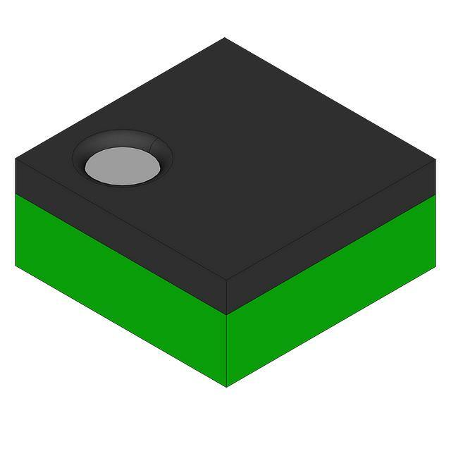
WLCSP9 1.215x1.215x0.581
CASE 567QW
ISSUE O
DATE 31 OCT 2016
DOCUMENT NUMBER:
STATUS:
98AON13355G
ON SEMICONDUCTOR STANDARD
NEW STANDARD:
© Semiconductor Components Industries, LLC, 2002
October, DESCRIPTION:
2002 − Rev. 0
http://onsemi.com
WLCSP9 1.215x1.215x0.581 1
Electronic versions are uncontrolled except when
accessed directly from the Document Repository. Printed
versions are uncontrolled except when stamped
“CONTROLLED COPY” in red.
Case Outline Number:
PAGE 1 OFXXX
2
�DOCUMENT NUMBER:
98AON13355G
PAGE 2 OF 2
ISSUE
O
REVISION
RELEASED FOR PRODUCTION FROM FAIRCHILD UC009AK TO ON SEMICONDUCTOR. REQ. BY F. ESTRADA.
DATE
31 OCT 2016
ON Semiconductor and
are registered trademarks of Semiconductor Components Industries, LLC (SCILLC). SCILLC reserves the right to make changes without further notice
to any products herein. SCILLC makes no warranty, representation or guarantee regarding the suitability of its products for any particular purpose, nor does SCILLC assume any liability
arising out of the application or use of any product or circuit, and specifically disclaims any and all liability, including without limitation special, consequential or incidental damages.
“Typical” parameters which may be provided in SCILLC data sheets and/or specifications can and do vary in different applications and actual performance may vary over time. All
operating parameters, including “Typicals” must be validated for each customer application by customer’s technical experts. SCILLC does not convey any license under its patent rights
nor the rights of others. SCILLC products are not designed, intended, or authorized for use as components in systems intended for surgical implant into the body, or other applications
intended to support or sustain life, or for any other application in which the failure of the SCILLC product could create a situation where personal injury or death may occur. Should
Buyer purchase or use SCILLC products for any such unintended or unauthorized application, Buyer shall indemnify and hold SCILLC and its officers, employees, subsidiaries, affiliates,
and distributors harmless against all claims, costs, damages, and expenses, and reasonable attorney fees arising out of, directly or indirectly, any claim of personal injury or death
associated with such unintended or unauthorized use, even if such claim alleges that SCILLC was negligent regarding the design or manufacture of the part. SCILLC is an Equal
Opportunity/Affirmative Action Employer. This literature is subject to all applicable copyright laws and is not for resale in any manner.
© Semiconductor Components Industries, LLC, 2016
October, 2016 − Rev. O
Case Outline Number:
567QW
�ON Semiconductor and
are trademarks of Semiconductor Components Industries, LLC dba ON Semiconductor or its subsidiaries in the United States and/or other countries.
ON Semiconductor owns the rights to a number of patents, trademarks, copyrights, trade secrets, and other intellectual property. A listing of ON Semiconductor’s product/patent
coverage may be accessed at www.onsemi.com/site/pdf/Patent−Marking.pdf. ON Semiconductor reserves the right to make changes without further notice to any products herein.
ON Semiconductor makes no warranty, representation or guarantee regarding the suitability of its products for any particular purpose, nor does ON Semiconductor assume any liability
arising out of the application or use of any product or circuit, and specifically disclaims any and all liability, including without limitation special, consequential or incidental damages.
Buyer is responsible for its products and applications using ON Semiconductor products, including compliance with all laws, regulations and safety requirements or standards,
regardless of any support or applications information provided by ON Semiconductor. “Typical” parameters which may be provided in ON Semiconductor data sheets and/or
specifications can and do vary in different applications and actual performance may vary over time. All operating parameters, including “Typicals” must be validated for each customer
application by customer’s technical experts. ON Semiconductor does not convey any license under its patent rights nor the rights of others. ON Semiconductor products are not
designed, intended, or authorized for use as a critical component in life support systems or any FDA Class 3 medical devices or medical devices with a same or similar classification
in a foreign jurisdiction or any devices intended for implantation in the human body. Should Buyer purchase or use ON Semiconductor products for any such unintended or unauthorized
application, Buyer shall indemnify and hold ON Semiconductor and its officers, employees, subsidiaries, affiliates, and distributors harmless against all claims, costs, damages, and
expenses, and reasonable attorney fees arising out of, directly or indirectly, any claim of personal injury or death associated with such unintended or unauthorized use, even if such
claim alleges that ON Semiconductor was negligent regarding the design or manufacture of the part. ON Semiconductor is an Equal Opportunity/Affirmative Action Employer. This
literature is subject to all applicable copyright laws and is not for resale in any manner.
PUBLICATION ORDERING INFORMATION
LITERATURE FULFILLMENT:
Literature Distribution Center for ON Semiconductor
19521 E. 32nd Pkwy, Aurora, Colorado 80011 USA
Phone: 303−675−2175 or 800−344−3860 Toll Free USA/Canada
Fax: 303−675−2176 or 800−344−3867 Toll Free USA/Canada
Email: orderlit@onsemi.com
◊
N. American Technical Support: 800−282−9855 Toll Free
USA/Canada
Europe, Middle East and Africa Technical Support:
Phone: 421 33 790 2910
ON Semiconductor Website: www.onsemi.com
Order Literature: http://www.onsemi.com/orderlit
For additional information, please contact your local
Sales Representative
�