High-Current, High & Low-Side,
Gate-Driver IC
FAN73912A
Description
The FAN73912A is a monolithic high and low−side gate−drive IC
designed for high−voltage and high−speed driving for MOSFETs
and IGBTs that operate up to +1200 V.
The advanced input filter of HIN provides protection against
short−pulsed input signals caused by noise.
An advanced level−shift circuit offers high−side gate driver
operation up to VS = −9.8 V (typical) for VBS = 15 V. The UVLO
circuit prevents malfunction when VCC and VBS are lower than
the specified threshold voltage.
Output drivers typically source and sink 2 A and 3 A, respectively.
www.onsemi.com
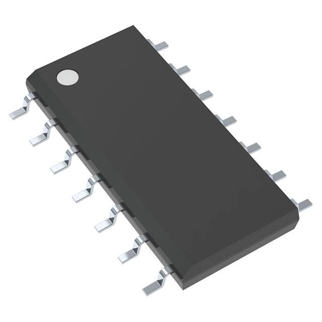
SOIC−16
CASE 751BH
Features
• Floating Channel for Bootstrap Operation to +1200 V
• Typically 2 A/ 3 A Sourcing/Sinking Current Driving Capability for
•
•
•
•
•
•
•
•
•
•
Both Channels
Gate Driver Supply (VCC) Range from 12 V to 20 V
Separate Logic Supply (VDD) Range from 3 V to 20 V
Extended Allowable Negative VS Swing to −9.8 V for Signal
Propagation at VCC = VBS = 15 V
Built−in Cycle−by−Cycle Edge−Triggered Shutdown Logic
Common−Mode dv/dt Noise Canceling Circuit
UVLO Functions for Both Channels
Built−in Advanced Input Filter
Matched Propagation Delay Below 60 ns
Outputs in−Phase with Input Signal
Logic and Power Ground ±10 V Offset
Electrical Contactor
Industrial Motor Driver
UPS
Solar Inverter
Ballast
General−Purpose Half−Bridge Topology
© Semiconductor Components Industries, LLC, 2020
February, 2021 − Rev. 1
FAN73912A
ON
LOT No.
ORDERING INFORMATION
Device
FAN73912AMX
(Note 1)
Package
Shipping†
Wide−16
SOIC
1,000/
Tape & Reel
†For information on tape and reel specifications,
including part orientation and tape sizes, please
refer to our Tape and Reel Packaging Specification
Brochure, BRD8011/D.
1. This device passed wave−soldering test by
JESD22A−111
Typical Application
•
•
•
•
•
•
MARKING DIAGRAM
1
Publication Order Number:
FAN73912A/D
�FAN73912A
Up to 1200 V
Q1
Typically
3.3~15 V
Controller
R1
9 NC
HO 8
10 NC
VB
7
11 VDD
VS
6
HIN
12 HIN
NC
5
DBOOT
SD
13 SD
NC
4
RBOOT
LIN
14 LIN
VCC
3
15 VSS
COM
2
CBOOT
Load
15 V
C1
Q2
R2
16 NC
1
LO
Figure 1. Application Schematic − Adjustable Option
7 VB
UVLO
LIN 14
SCHMITT
TRIGGER
INPUT
VSS/COM
LEVEL
SHIFT
CYCLE−By−
CYCLE EDGE
TRIGGERED
SHUTDOWN
NOISE
CANCELLER
8 HO
6 VS
3 VCC
UVLO
DELAY
LS(ON/OFF)
DRIVER
SD 13
VSS 15
R R
S
Q
DRIVER
HIN 12
PULSE
GENERATOR
HS(ON/OFF)
VDD 11
1 LO
2 COM
Pin 4,5,9,10 and 16 are no connection
Figure 2. Simplified Block Diagram
www.onsemi.com
2
�FAN73912A
LO
1
16 NC
COM
2
15 VSS
FAN73912A
VCC 3
14 LIN
NC
4
13 SD
NC
5
12 HIN
VS
6
11 V
DD
VB
7
10 NC
HO
8
9
NC
Figure 3. Pin Connections − Wide 16−SOIC
(Top View)
Table 1. PIN FUNCTION DESCRIPTION (Note 2)
ÁÁÁÁÁÁÁÁÁÁÁÁÁÁÁÁÁÁÁÁÁÁÁÁÁÁÁÁÁÁÁÁÁÁÁ
ÁÁÁÁÁÁÁÁÁÁÁÁÁÁÁÁÁÁÁÁÁÁÁÁÁÁÁÁÁÁÁÁÁÁÁ
ÁÁÁÁÁÁÁÁÁÁÁÁÁÁÁÁÁÁÁÁÁÁÁÁÁÁÁÁÁÁÁÁÁÁÁ
ÁÁÁÁÁÁÁÁÁÁÁÁÁÁÁÁÁÁÁÁÁÁÁÁÁÁÁÁÁÁÁÁÁÁÁ
ÁÁÁÁÁÁÁÁÁÁÁÁÁÁÁÁÁÁÁÁÁÁÁÁÁÁÁÁÁÁÁÁÁÁÁ
ÁÁÁÁÁÁÁÁÁÁÁÁÁÁÁÁÁÁÁÁÁÁÁÁÁÁÁÁÁÁÁÁÁÁÁ
ÁÁÁÁÁÁÁÁÁÁÁÁÁÁÁÁÁÁÁÁÁÁÁÁÁÁÁÁÁÁÁÁÁÁÁ
ÁÁÁÁÁÁÁÁÁÁÁÁÁÁÁÁÁÁÁÁÁÁÁÁÁÁÁÁÁÁÁÁÁÁÁ
ÁÁÁÁÁÁÁÁÁÁÁÁÁÁÁÁÁÁÁÁÁÁÁÁÁÁÁÁÁÁÁÁÁÁÁ
ÁÁÁÁÁÁÁÁÁÁÁÁÁÁÁÁÁÁÁÁÁÁÁÁÁÁÁÁÁÁÁÁÁÁÁ
ÁÁÁÁÁÁÁÁÁÁÁÁÁÁÁÁÁÁÁÁÁÁÁÁÁÁÁÁÁÁÁÁÁÁÁ
ÁÁÁÁÁÁÁÁÁÁÁÁÁÁÁÁÁÁÁÁÁÁÁÁÁÁÁÁÁÁÁÁÁÁÁ
ÁÁÁÁÁÁÁÁÁÁÁÁÁÁÁÁÁÁÁÁÁÁÁÁÁÁÁÁÁÁÁÁÁÁÁ
ÁÁÁÁÁÁÁÁÁÁÁÁÁÁÁÁÁÁÁÁÁÁÁÁÁÁÁÁÁÁÁÁÁÁÁ
ÁÁÁÁÁÁÁÁÁÁÁÁÁÁÁÁÁÁÁÁÁÁÁÁÁÁÁÁÁÁÁÁÁÁÁ
ÁÁÁÁÁÁÁÁÁÁÁÁÁÁÁÁÁÁÁÁÁÁÁÁÁÁÁÁÁÁÁÁÁÁÁ
ÁÁÁÁÁÁÁÁÁÁÁÁÁÁÁÁÁÁÁÁÁÁÁÁÁÁÁÁÁÁÁÁÁÁÁ
Pin No.
Symbol
1
LO
Low−Side Driver Output
2
COM
Low−Side Driver Return
3
VCC
Low−Side Supply Voltage
4
NC
No Connection
5
NC
No Connection
6
VS
High−Voltage Floating Supply Return
7
VB
High−Side Floating Supply
8
HO
High−Side Driver Output
9
NC
No Connection
10
NC
No Connection
11
VDD
Logic Supply Voltage
12
HIN
Logic Input for High−Side Gate Driver Output
13
SD
Logic Input for Shutdown
14
LIN
Logic Input for Low−Side Gate Driver Output
15
VSS
Logic Ground
16
NC
No Connection
Description
2. Do not connect NC pins to ground or any other nodes in the circuitry to ensure floating status.
www.onsemi.com
3
�FAN73912A
Table 2. MAXIMUM RATINGS (TJ = 25°C, unless otherwise specified. All voltage parameters are referenced to COM unless
otherwise stated in the table.)
Parameter
Symbol
Min
Max
Unit
−0.3
1225.0
V
VB − 25
VB − 25
VB − 23
VB + 0.3
VB + 0.3
VB + 0.3
VB
High−Side Floating Supply Voltage
VS
High−Side Floating Offset Voltage
VHO
High−Side Floating Output Voltage
VS − 0.3
VB + 0.3
V
VCC
Low−Side Supply Voltage
−0.3
25
V
VLO
Low−Side Floating Output Voltage
−0.3
VCC + 0.3
V
VDD
Logic Supply Voltage
−0.3
VSS − 0.3
25
VSS + 25
V
VSS
Logic GND
VDD − 25
VDD + 0.3
V
VIN
Logic Input Voltage (HIN, LIN and SD)
−0.3
VSS + VDD − 25.3
25
VDD + 0.3
V
Allowable Offset Voltage Slew Rate
−
±50
V/ns
Power Dissipation
−
1.3
W
qJA
Thermal Resistance
−
95
°C/W
TJ
Junction Temperature
−
150
°C
TSTG
Storage Temperature
−55
150
°C
dVS/dt
PD
(Note 3, 4, 5)
TJ = 150°C
TJ = 25°C
TJ =−40°C
V
Stresses exceeding those listed in the Maximum Ratings table may damage the device. If any of these limits are exceeded, device functionality
should not be assumed, damage may occur and reliability may be affected.
3. Mounted on 76.2 x 114.3 x 1.6 mm PCB (FR−4 glass epoxy material).
4. Refer to the following standards:
JESD51−2: Integral circuit’s thermal test method environmental conditions, natural convection;
JESD51−3: Low effective thermal conductivity test board for leaded surface−mount packages.
5. Do not exceed maximum power dissipation (PD) under any circumstances.
Table 3. RECOMMENDED OPERATING CONDITIONS (All voltage parameters are referenced to COM unless otherwise stated in
the table.)
Parameter
Symbol
Min
Max
Unit
VB
High−Side Floating Supply Voltage
VS + 12
VS + 20
V
VS
High−Side Floating Supply Offset Voltage (Note 6)
8 − VCC
1200
V
VHO
High−Side (HO) Output Voltage
VS
VB
V
VCC
Low−Side Supply Voltage
12
20
V
VLO
Low−Side (LO) Output Voltage
0
VCC
V
VDD
Logic Supply Voltage
VSS + 3
VSS + 20
V
VSS
Logic Ground (Note 7)
−10
10
V
VIN
Logic Input Voltage (HIN, LIN, SD)
0
VSS + VDD − 20
20
VDD
V
TJ
Junction Temperature
−40
+125
°C
Functional operation above the stresses listed in the Recommended Operating Ranges is not implied. Extended exposure to stresses beyond
the Recommended Operating Ranges limits may affect device reliability.
6. Referenced to TJ = 25°C.
7. When VDD < 10 V, the minimum VSS offset is limited to −VDD.
www.onsemi.com
4
�FAN73912A
Table 4. STATIC ELECTRICAL CHARACTERISTICS (VBIAS (VCC, VBS, VDD) = 15.0 V, TJ = −40°C to 125°C, unless otherwise
specified. The VIH, VIL and IIN parameters are referenced to VSS and are applicable to respective input leads: HIN, LIN and SD. The VO
and IO parameters are referenced to VS and COM and are applicable to the respective output leads: HO and LO. The VDDUV parameters
are referenced to COM. The VBSUV parameters are referenced to VS1, 2, 3)
Symbol
Parameter
Conditions
Min
Typ
Max
Units
TJ = 25°C
−
170
300
mA
TJ = −40°C to 125°C
−
170
350
TJ = 25°C
−
−
10
TJ = −40°C to 125°C
−
−
20
LOW−SIDE POWER SUPPLY SECTION
IQCC
IQDD
Quiescent VCC Supply Current
Quiescent VDD Supply Current
VIN = 0 V or VDD
VIN = 0 V or VDD
mA
IPCC
Operating VCC Supply Current
fIN = 20 kHz, rms VIN = 15 VPP
−
650
950
IPDD
Operating VDD Supply Current
fIN = 20 kHz, rms VIN = 15 VPP
−
2
−
Shutdown Supply Current
SD = VDD
−
30
50
mA
VCCUV+
VCC Supply Under−Voltage
Positive−Going Threshold Voltage
VCC = Sweep
9.7
11.0
12
V
VCCUV−
VCC Supply Under−Voltage
Negative−Going Threshold Voltage
VCC = Sweep
9.2
10.5
11.4
V
VCCUVH
VCC Supply Under−Voltage Lockout
Hysteresis Voltage
VCC = Sweep
−
0.5
−
V
ISD
mA
BOOTSTRAPPED SUPPLY SECTION
IQBS
Quiescent VBS Supply Current
VIN = 0 V or VDD
−
50
100
mA
IPBS
Operating VBS Supply Current
fIN = 20 kHz, rms value
−
550
850
mA
VBSUV+
VBS Supply Under−Voltage
Positive−Going Threshold Voltage
VBS = Sweep
9.7
11.0
12.0
V
VBSUV−
VBS Supply Under−Voltage
Negative−Going Threshold Voltage
VBS = Sweep
9.2
10.5
11.4
V
VBSUVH
VBS Supply Under−Voltage Lockout
Hysteresis Voltage
VBS = Sweep
−
0.5
−
V
Offset Supply Leakage Current
VB = VS = 1200 V (TJ = 25°C)
−
−
100
mA
VB = VS = 1200 V (TJ = 125°C) (Note 8)
−
−
100
VB = VS = 1000 V (TJ = −40°C) (Note 8)
−
−
100
2.4
−
−
TJ = 25°C
9.5
−
−
TJ = −40°C to 125°C
10.5
−
−
ILK
INPUT LOGIC SECTION (HIN.LIN AND AD)
VIH
Logic “1” Input Voltage
VDD = 3 V
VDD = 15 V
VIL
Logic “0” Input Voltage
VDD = 3 V
VDD = 15 V
−
−
0.8
TJ = 25°C
−
−
6.0
TJ = −40°C to 125°C
−
−
9.5
V
V
IIN+
Logic “1” Input bias Current
VIN = 15 V
−
30
50
mA
IIN−
Logic “0” Input bias Current
VIN = 0 V
−
−
1
mA
RIN
Logic Input Pull−down Resistance
−
500
−
kW
TJ = 25°C
−
−
1.2
V
TJ = −40°C to 125°C
−
−
1.4
−
−
0.1
GATE DRIVER OUTPUT SECTION
VOH
VOL
High−Level Output Voltage,
VBIAS−VO
IO = 0 A
Low−Level Output Voltage, VO
IO = 0 A
V
Product parametric performance is indicated in the Electrical Characteristics for the listed test conditions, unless otherwise noted. Product
performance may not be indicated by the Electrical Characteristics if operated under different conditions.
8. These parameters are guaranteed by design.
www.onsemi.com
5
�FAN73912A
Table 4. STATIC ELECTRICAL CHARACTERISTICS (VBIAS (VCC, VBS, VDD) = 15.0 V, TJ = −40°C to 125°C, unless otherwise
specified. The VIH, VIL and IIN parameters are referenced to VSS and are applicable to respective input leads: HIN, LIN and SD. The VO
and IO parameters are referenced to VS and COM and are applicable to the respective output leads: HO and LO. The VDDUV parameters
are referenced to COM. The VBSUV parameters are referenced to VS1, 2, 3) (continued)
Symbol
Parameter
Conditions
Min
Typ
Max
Units
GATE DRIVER OUTPUT SECTION
IO+
Output HIGH Short−Circuit Pulse
Current
VO = 0 V, VIN = 5 V with PW ≤ 10 ms
−
2.0
−
A
IO−
Output LOW Short−Circuit Pulsed
Current
VO = 15 V, VIN = 0 V with PW ≤ 10 ms
−
3.0
−
A
VS
Allowable Negative VS Pin Voltage
for HIN Signal Propagation to HO
−
−9.8
−7.0
V
Product parametric performance is indicated in the Electrical Characteristics for the listed test conditions, unless otherwise noted. Product
performance may not be indicated by the Electrical Characteristics if operated under different conditions.
8. These parameters are guaranteed by design.
Table 5. DYNAMIC ELECTRICAL CHARACTERISTICS (VBIAS(VCC, VBS, VDD) = 15.0 V, VS = VSS = COM, CL = 1000 pF and
TJ = −40°C to 125°C, unless otherwise specified.)
Symbol
Parameter
Conditions
Min
Typ
Max
Units
LOW−SIDE POWER SUPPLY SECTION
tON
Turn−On Propagation Delay
VS = 0 V
−
500
−
ns
tOFF
Turn−Off Propagation Delay
VS = 0 V
−
550
−
ns
tFLTIN
Input Filtering Time (HIN, LIN)
(Note 9)
TJ = 25°C
80
150
220
ns
TJ = −40°C to 125°C
80
150
300
−
30
−
ns
TJ = 25°C
260
330
400
ns
TJ = −40°C to 125°C
200
330
550
−
25
−
tFLTSD
tSD
Input Filtering Time (SD)
Shutdown Propagation Delay Time
tR
Turn−On Rise Time
tF
Turn−Off Fall Time
MT
PM
−
15
−
Delay Matching ,
HO & LO Turn−On/OFF (Note 10)
TJ = 25°C
−
−
50
TJ = −40°C to 125°C
−
−
60
Output Pulse−Width Matching
(Note 11)
PWIN > 1 ms
TJ = 25°C
−
50
100
TJ = −40°C to 125°C
−
50
140
ns
ns
ns
Product parametric performance is indicated in the Electrical Characteristics for the listed test conditions, unless otherwise noted. Product
performance may not be indicated by the Electrical Characteristics if operated under different conditions.
9. The minimum width of the input pulse should exceed 500 ns to ensure the filtering time of the input filter is exceeded.
10. MT is defined as an absolute value of matching delay time between High−side and Low−Side.
11. PM is defined as an absolute value of matching pulse−width between Input and Output.
www.onsemi.com
6
�FAN73912A
TYPICAL CHARACTERISTICS
580
660
560
640
620
tOFF [ns]
tON [ns]
540
520
500
600
580
560
540
480
520
460
500
440
−40
−20
0
20
40
60
80
480
−40
100 120
−20
0
30
25
25
20
20
tF [ns]
tR [ns]
30
15
10
5
5
20
40
60
80
100
0
−40
120
−20
0
Figure 6. Turn−On Rise Time vs Temperature
120
20
40
60
80
100
120
Figure 7. Turn−Off Fall Time vs. Temperature
50
50
40
40
MTOFF [ns]
MTON [ns]
100
Temperature [°C]
Temperature [°C]
30
20
10
0
−40
80
15
10
0
60
Figure 5. Turn−Off Propagation Delay
vs. Temperature
Figure 4. Turn−On Propagation Delay
vs. Temperature
−20
40
Temperature [°C]
Temperature [°C]
0
−40
20
30
20
10
−20
0
20
40
60
80
100
0
−40
120
−20
0
20
40
60
80
100
Temperature [°C]
Temperature [°C]
Figure 9. Turn−Off Delay Matching
vs. Temperature
Figure 8. Turn−On Delay Matching
vs. Temperature
www.onsemi.com
7
120
�FAN73912A
TYPICAL CHARACTERISTICS (continued)
40
440
420
30
380
IIN+ [mA]
tSD [ns]
400
360
340
320
20
10
300
280
260
−40
−20
0
20
40
60
80
100
0
−40
120
−20
0
80
100
120
2.0
VHIN = VLIN = 0 V
VHIN = VDD, VLIN = 0 V
(or VHIN = 0 V, VLIN = VDD)
VHIN = VLIN = 0 V
VHIN = VDD, VLIN = 0 V
(or VHIN = 0 V, VLIN = VDD)
1.8
1.6
1.4
IQDD [mA]
IQCC [mA]
60
Figure 11. Logic Input High Bias Current
vs. Temperature
Figure 10. Shutdown Propagation Delay
vs. Temperature
1.2
1.0
0.8
0.6
0.4
0.2
−20
0
20
40
60
80
100
0.0
−40
120
−20
0
20
40
60
80
100
120
Temperature [°C]
Temperature [°C]
Figure 13. Quiescent VDD Supply Current
vs. Temperature
Figure 12. Quiescent VCC Supply Current
80
800
70
700
60
600
50
IPCC [mA]
IQBS [mA]
40
Temperature [°C]
Temperature [°C]
220
210
200
190
180
170
160
150
140
130
120
110
100
90
−40
20
40
30
500
400
20
300
10
0
−40
−20
0
20
40
60
80
100
200
−40
120
−20
0
20
40
60
80
100
Temperature [°C]
Temperature [°C]
Figure 15. Operating VCC Supply Current
Figure 14. Quiescent VBS Supply Current
www.onsemi.com
8
120
�FAN73912A
TYPICAL CHARACTERISTICS (continued)
5.0
4.5
1000
800
3.5
IPBS [mA]
IPDD [mA]
4.0
3.0
2.5
2.0
1.5
1.0
600
400
200
0.5
0.0
−40
−20
0
20
40
60
80
100
0
−40
120
−20
0
60
80
100
120
Figure 17. Operating VBS Supply Current
vs. Temperature
Figure 16. Operating VDD Supply Current
11.0
11.4
10.8
11.2
11.0
VCCUV− [V]
VCCUV+ [V]
40
Temperature [°C]
Temperature [°C]
10.8
10.6
10.6
10.4
10.2
10.0
10.4
9.8
10.2
9.6
10.0
−40
−20
0
20
40
60
80
100
−40
120
−20
0
20
40
60
80
100
120
Temperature [°C]
Temperature [°C]
Figure 19. VCC UVLO− vs. Temperature
Figure 18. VCC UVLO+ vs Temperature
11.0
11.4
10.8
11.2
10.6
11.0
VBSUV− [V]
VBSUV+ [V]
20
10.8
10.6
10.4
10.4
10.2
10.0
9.8
10.2
10.0
−40
9.6
−20
0
20
40
60
80
100
−40
120
−20
0
20
40
60
80
100
Temperature [°C]
Temperature [°C]
Figure 21. VBS UVLO− vs. Temperature
Figure 20. VBS UVLO+ vs. Temperature
www.onsemi.com
9
120
�FAN73912A
TYPICAL CHARACTERISTICS (continued)
0.010
0.008
1.2
0.006
1.0
0.004
VOL [V]
VOH [V]
1.4
0.8
0.6
0.002
0.000
−0.002
−0.004
0.4
−0.006
0.2
−0.008
0.0
−40
−20
0
20
40
60
80
100
−0.010
−40
120
−20
0
20
Temperature [°C]
10
9
9
8
7
VIL− [V]
VIH [V]
6
5
5
4
3
3
2
2
40
60
80
100
1
−40
120
−20
0
20
60
80
100
120
Figure 25. Logic Low Input Voltage
vs. Temperature
Figure 24. Logic High Input Voltage
−7
Logic Threshold Voltage [V]
12
−8
VS [V]
40
Temperature [°C]
Temperature [°C]
−9
−10
−11
−12
−40
120
VDD = 15 V
VDD = 3 V
6
4
20
100
8
VDD=15 V
VDD =3 V
7
0
80
Figure 23. Low−Level Output Voltage
vs. Temperature
10
−20
60
Temperature [°C]
Figure 22. High−Level Output Voltage
1
−40
40
−20
0
20
40
60
80
100
10
8
6
4
0
120
VIH
VIL
2
0
2
4
6
8
10
12
14
16
18
VDD Logic Supply Voltage [V]
Temperature [°C]
Figure 27. Input Logic (HIN&LIN) Threshold
vs. VDD Supply Voltage
Figure 26. Allowable Negative VS
vs. Temperature
www.onsemi.com
10
20
�FAN73912A
TYPICAL CHARACTERISTICS (continued)
−4
VS [V]
−8
tON [ns]
VCC = VSS
VCOM = 0 V
TA = 25°C
−6
−10
−12
−14
−16
10
11
12
13
14
15
16
17
18
19
20
600
580
560
540
520
500
480
460
440
420
400
Figure 29. Turn−On Propagation Delay
vs. VDD Supply Voltage
350
High Side
Low Side
250
200
150
100
50
0
3 4 5 6 7 8 9 10 11 12 13 14 15 16 17 18 19 20
Figure 31. Logic Input Filtering Time
vs. VDD Supply Voltage
Figure 30. Turn−Off Propagation Delay
vs. VDD Supply Voltage
160
Positive
Negative
140
120
3 4 5 6 7 8 9 10 11 12 13 14 15 16 17 18 19 20
VDD Supply Voltage [V]
VDD Supply Voltage [V]
100
tSD [V]
tFLTSD [ns]
Positive
Negative
300
tFLTIN [ns]
tOFF [ns]
Figure 28. Allowable Negative VS Voltage
for HIN Signal Propagation to High Side
vs. VCC Supply Voltage
80
60
40
20
0
3 4 5 6 7 8 9 10 11 12 13 14 15 16 17 18 19 20
VDD Supply Voltage [V]
VCC Supply Voltage [V]
600
580
560
540
520
500
480
460
440
420
400
High Side
Low Side
440
420
400
380
360
340
320
300
280
260
High Side
Low Side
3 4 5 6 7 8 9 10 11 12 13 14 15 16 17 18 19 20
3 4 5 6 7 8 9 10 11 12 13 14 15 16 17 18 19 20
VDD Supply Voltage [V]
VDD Supply Voltage [V]
Figure 33. Shutdown Propagation Delay
vs. VDD Supply Voltage
Figure 32. Shutdown Input Filtering
Time vs. VDD Supply Voltage
www.onsemi.com
11
�FAN73912A
TYPICAL CHARACTERISTICS (continued)
100
HighSide
LowSide
PM [ns]
80
60
40
20
0
3 4 5 6 7 8 9 10 11 12 13 14 15 16 17 18 19 20
VDD Supply Voltage [V]
Figure 34. Output Pulse−Width Matching vs. VDD Supply Voltage
SWITCHING TIME DEFINITIONS
9 NC
HO 8
10 NC
VB 7
11 VDD
VS 6
HIN
12 HIN
NC 5
SD
13 SD
NC 4
14 LIN
VCC 3
15 VSS
COM 2
16 NC
LO 1
15 V
LIN
HO
100 nF
1 nF
(0 to 1200 V)
15 V
100 nF
LO
1 nF
Figure 35. Switching Time Test Circuit
HIN
LIN
SD
HO
Skip
LO
Shutdown
Shutdown
Figure 36. Input/Output Timing Diagram
www.onsemi.com
12
15 V
�FAN73912A
HIN
50%
50%
LIN
tR
tON
tOFF
90%
tF
90%
HO
10%
10%
Figure 37. Switching Time Definition
50%
SD
tSD
90%
HO
(LO)
Figure 38. Shutdown Waveform Definition
50%
HIN
50%
LIN
LO
10%
MT
HO
10%
90%
LO
MT
Figure 39. Delay Matching Waveform Definitions
www.onsemi.com
13
90%
HO
�FAN73912A
APPLICATIONS INFORMATION
Shutdown Input
Short−Pulsed Input Noise Rejection Method
When the SD pin is in LOW state, the gate driver operates
normally. When a condition occurs that should shut down
the gate driver, the SD pin should be HIGH. The Shutdown
circuitry has an input filter; the minimum input duration is
specified by tFLTIN (typically 250 ns).
The input filter circuitry provides protection against
short−pulsed input signals (HIN, LIN, and SD) on the input
signal lines by applied noise signal.
If the input signal duration is less than input filter time
(tFLTIN), the output does not change states.
Example A and B of the Figure 42 show the input
and output waveforms with short−pulsed noise spikes
with a duration less than input filter time; the output does not
change states.
50%
SD
Example A
tSD
90%
HO
(LO)
IN
tFLTIN
tFLTIN
tFLTIN
tFLTIN
tFLTIN
tFLTIN
OUT
(LOW)
Figure 40. Output Shutdown Timing Waveform
Example B
Noise Filter
Input Noise Filter
Figure 41 shows the input noise filter method, which has
symmetry duration between the input signal (tINPUT)
and the output signal (tOUTPUT) and helps to reject noise
spikes and short pulses. This input filter is applied to
the HIN, LIN, and EN inputs. The upper pair of waveforms
(Example A) shows an input signal duration (tINPUT) much
longer than input filter time (tFLTIN); it is approximately
the same duration between the input signal time (tINPUT)
and the output signal time (tOUTPUT). The lower pair
of waveforms (Example B) shows an input signal time
(tINPUT) slightly longer than input filter time (tFLTIN); it is
approximately the same duration between input signal time
(tINPUT) and the output signal time (tOUTPUT).
Example A
IN
OUT
(HIGH)
Figure 42. Noise Rejecting Input Filter Definition
Negative VS Transient
The bootstrap circuit has the advantage of being simple
and low cost, but has some limitations. The biggest difficulty
with this circuit is the negative voltage present at the emitter
of the high−side switching device when high−side switch is
turned−off in half−bridge application. If the high−side
switch, Q1, turns−off while the load current is flowing to
an inductive load, a current commutation occurs from
high−side switch, Q1, to the diode, D2, in parallel with
the low−side switch of the same inverter leg. Then
the negative voltage present at the emitter of the high−side
switching device, just before the freewheeling diode, D2,
starts clamping, causes load current to suddenly flow to
the low−side freewheeling diode, D2, as shown in Figure 43.
tFLTIN
tINPUT
tOUTPUT
DC+ Bus
Q1
OUT
D1
iLOAD
ifreewheeling
Example B
IN
tFLTIN
Load
tINPUT
tOUTPUT
OUT
Q2
Output duration is
same as input duration
D2
Figure 43. Half−Bridge Application Circuits
Figure 41. Input Noise Filter Definition
www.onsemi.com
14
�FAN73912A
This negative voltage can be trouble for the gate driver’s
output stage, there is the possibility to develop
an over−voltage condition of the bootstrap capacitor, input
signal missing and latch−up problems because it directly
affects the source VS pin of the gate driver, shown
in Figure 44. This undershoot voltage is called “negative VS
transient”.
DC+ Bus
LC1
Q1
LC2
Q2
D1
D2
ifreewheeling
LE1
VS1
−
LC3 VLC3
+
Q3
D3
Q1
iLOAD
Load
LE2
+
VLC4
−
VS2
LC4
Q4
D4
−
LE3 VLE3
+
+
VLE4
−
LE4
Figure 46. Q1 Turn−Off and D3 Conducting
VS
GND
The FAN73912A has a typical negative VS transient
characteristics, as shown in Figure 47.
Freewheeling
Figure 44. VS Waveforms During Q1 Turn−Off
VS [V]
Figure 45 and Figure 46 show the commutation of the load
current between high−side switch, Q1, and low−side
freewheeling diode, D3, in same inverter leg. The parasitic
inductances in the inverter circuit from the die wire bonding
to the PCB tracks are jumped together in LC and LE for each
IGBT. When the high−side switch, Q1, and low−side switch,
Q4, are turned on, the VS1 node is below DC+ voltage by
the voltage drops associated with the power switch
and the parasitic inductances of the circuit due to load
current is flows from Q1 and Q4, as shown in Figure 45.
When thehigh−side switch, Q1, is turned off and Q4,
remained turned on, the load current to flows the low−side
freewheeling diode, D3, due to the inductive load connected
to VS1 as shown in Figure 46. Q1 Turn−Off and D3
Conducting. The current flows from ground (which is
connected to the COM pin of the gate driver) to the load
and the negative voltage present at the emitter
of the high−side switching device. In this case, the COM pin
of the gate driver is at a higher potential than the VS pin due
to the voltage drops associated with freewheeling diode, D3,
and parasitic elements, LC3 and LE3.
VS1
+
VLC1
−
150
200
250
300
Figure 47. Negative VS Transient Characteristic
Even though the FAN73912A has been shown able to
handle these negative VS transient conditions, it is strongly
recommended that the circuit designer limit the negative VS
transient as much as possible by careful PCB layout to
minimize the value of parasitic elements and component
use. The amplitude of negative VS voltage is proportional to
the parasitic inductances and the turn−off speed, di/dt, of the
switching device.
D3
Printed Circuit Board Layout
The layout recommended for minimized parasitic
elements is as follows:
• Direct tracks between switches with no loops or
deviation.
• Avoid interconnect links. These can add significant
inductance.
• Reduce the effect of lead−inductance by lowering
package height above the PCB.
• Consider co−locating both power switches to reduce
track length.
LC2
Q2
iLOAD
+
ifreewheeling
VLE1
−
Load
LC3
Q3
LE3
100
General Guidelines
D1
LE1
50
Pulse Width [ns]
DC+ Bus
LC1
Q1
0
−20
−40
−60
−80
−100
−120
−140
−160
−180
−200
−220
D2
LE2
+
VLC4
−
VS2
LC4
Q4
D4
+
VLE4
−
LE4
Figure 45. Q1 and Q4 Turn−On
www.onsemi.com
15
�FAN73912A
• To minimize noise coupling, the ground plane should
•
not be placed under or near the high−voltage floating
side.
To reduce the EM coupling and improve the power
switch turn−on/off performance, the gate drive loops
must be reduced as much as possible.
•
Placement of Components
The recommended placement and selection of component
as follows:
• Place a bypass capacitor between the VCC and VSS
pins. A ceramic 1 mF capacitor is suitable for most
applications. This component should be placed as close
as possible to the pins to reduce parasitic elements.
• The bypass capacitor from VCC to VSS supports both
the low−side driver and bootstrap capacitor recharge.
A value at least ten times higher than the bootstrap
capacitor is recommended.
• The bootstrap resistor, RBOOT, must be considered in
sizing the bootstrap resistance and the current
developed during initial bootstrap charge. If the resistor
is needed in series with the bootstrap diode, verify that
VB does not fall below COM (ground). Recommended
•
•
•
•
use is typically 5 ~ 10 W that increase the VBS time
constant. If the voltage drop of bootstrap resistor
and diode is too high or the circuit topology does not
allow a sufficient charging time, a fast recovery or
ultra−fast recovery diode can be used.
The bootstrap capacitor, CBOOT, uses a low−ESR
capacitor, such as ceramic capacitor. It is strongly
recommended that the placement of components is as
follows:
Place components tied to the floating voltage pins (VB
and VS) near the respective high−voltage portions of
the device and the FAN73912A. Not Connected (NC)
pins in this package maximize the distance between
the high−voltage and low−voltage pins (see Figure 3).
Place and route for bypass capacitors and gate resistors
as close as possible to gate drive IC.
Locate the bootstrap diode, DBOOT, as close as possible
to bootstrap capacitor, CBOOT.
The bootstrap diode must use a lower forward voltage
drop and minimal switching time as soon as possible
for fast recovery or ultra−fast diode.
www.onsemi.com
16
�MECHANICAL CASE OUTLINE
PACKAGE DIMENSIONS
SOIC−16, 300 mils
CASE 751BH−01
ISSUE A
DATE 18 MAR 2009
D
SYMBOL
E1 E
MIN
NOM
MAX
2.49
2.64
A
2.36
A1
0.10
b
0.33
0.41
0.51
c
0.18
0.23
0.28
D
10.08
10.31
10.49
E
10.01
10.31
10.64
E1
7.39
7.49
7.59
0.30
1.27 BSC
e
h
0.25
L
0.38
θ
0º
0.75
0.81
1.27
8º
PIN #1 IDENTIFICATION
TOP VIEW
h
A
b
e
A1
SIDE VIEW
c
q
L
END VIEW
Notes:
(1) All dimensions are in millimeters. Angles in degrees.
(2) Complies with JEDEC MS-013.
DOCUMENT NUMBER:
DESCRIPTION:
98AON34279E
SOIC−16, 300 MILS
Electronic versions are uncontrolled except when accessed directly from the Document Repository.
Printed versions are uncontrolled except when stamped “CONTROLLED COPY” in red.
PAGE 1 OF 1
ON Semiconductor and
are trademarks of Semiconductor Components Industries, LLC dba ON Semiconductor or its subsidiaries in the United States and/or other countries.
ON Semiconductor reserves the right to make changes without further notice to any products herein. ON Semiconductor makes no warranty, representation or guarantee regarding
the suitability of its products for any particular purpose, nor does ON Semiconductor assume any liability arising out of the application or use of any product or circuit, and specifically
disclaims any and all liability, including without limitation special, consequential or incidental damages. ON Semiconductor does not convey any license under its patent rights nor the
rights of others.
© Semiconductor Components Industries, LLC, 2019
www.onsemi.com
�onsemi,
, and other names, marks, and brands are registered and/or common law trademarks of Semiconductor Components Industries, LLC dba “onsemi” or its affiliates
and/or subsidiaries in the United States and/or other countries. onsemi owns the rights to a number of patents, trademarks, copyrights, trade secrets, and other intellectual property.
A listing of onsemi’s product/patent coverage may be accessed at www.onsemi.com/site/pdf/Patent−Marking.pdf. onsemi reserves the right to make changes at any time to any
products or information herein, without notice. The information herein is provided “as−is” and onsemi makes no warranty, representation or guarantee regarding the accuracy of the
information, product features, availability, functionality, or suitability of its products for any particular purpose, nor does onsemi assume any liability arising out of the application or use
of any product or circuit, and specifically disclaims any and all liability, including without limitation special, consequential or incidental damages. Buyer is responsible for its products
and applications using onsemi products, including compliance with all laws, regulations and safety requirements or standards, regardless of any support or applications information
provided by onsemi. “Typical” parameters which may be provided in onsemi data sheets and/or specifications can and do vary in different applications and actual performance may
vary over time. All operating parameters, including “Typicals” must be validated for each customer application by customer’s technical experts. onsemi does not convey any license
under any of its intellectual property rights nor the rights of others. onsemi products are not designed, intended, or authorized for use as a critical component in life support systems
or any FDA Class 3 medical devices or medical devices with a same or similar classification in a foreign jurisdiction or any devices intended for implantation in the human body. Should
Buyer purchase or use onsemi products for any such unintended or unauthorized application, Buyer shall indemnify and hold onsemi and its officers, employees, subsidiaries, affiliates,
and distributors harmless against all claims, costs, damages, and expenses, and reasonable attorney fees arising out of, directly or indirectly, any claim of personal injury or death
associated with such unintended or unauthorized use, even if such claim alleges that onsemi was negligent regarding the design or manufacture of the part. onsemi is an Equal
Opportunity/Affirmative Action Employer. This literature is subject to all applicable copyright laws and is not for resale in any manner.
PUBLICATION ORDERING INFORMATION
LITERATURE FULFILLMENT:
Email Requests to: orderlit@onsemi.com
onsemi Website: www.onsemi.com
◊
TECHNICAL SUPPORT
North American Technical Support:
Voice Mail: 1 800−282−9855 Toll Free USA/Canada
Phone: 011 421 33 790 2910
Europe, Middle East and Africa Technical Support:
Phone: 00421 33 790 2910
For additional information, please contact your local Sales Representative
�