Is Now Part of
To learn more about ON Semiconductor, please visit our website at
www.onsemi.com
Please note: As part of the Fairchild Semiconductor integration, some of the Fairchild orderable part numbers
will need to change in order to meet ON Semiconductor’s system requirements. Since the ON Semiconductor
product management systems do not have the ability to manage part nomenclature that utilizes an underscore
(_), the underscore (_) in the Fairchild part numbers will be changed to a dash (-). This document may contain
device numbers with an underscore (_). Please check the ON Semiconductor website to verify the updated
device numbers. The most current and up-to-date ordering information can be found at www.onsemi.com. Please
email any questions regarding the system integration to Fairchild_questions@onsemi.com.
ON Semiconductor and the ON Semiconductor logo are trademarks of Semiconductor Components Industries, LLC dba ON Semiconductor or its subsidiaries in the United States and/or other countries. ON Semiconductor owns the rights to a number
of patents, trademarks, copyrights, trade secrets, and other intellectual property. A listing of ON Semiconductor’s product/patent coverage may be accessed at www.onsemi.com/site/pdf/Patent-Marking.pdf. ON Semiconductor reserves the right
to make changes without further notice to any products herein. ON Semiconductor makes no warranty, representation or guarantee regarding the suitability of its products for any particular purpose, nor does ON Semiconductor assume any liability
arising out of the application or use of any product or circuit, and specifically disclaims any and all liability, including without limitation special, consequential or incidental damages. Buyer is responsible for its products and applications using ON
Semiconductor products, including compliance with all laws, regulations and safety requirements or standards, regardless of any support or applications information provided by ON Semiconductor. “Typical” parameters which may be provided in ON
Semiconductor data sheets and/or specifications can and do vary in different applications and actual performance may vary over time. All operating parameters, including “Typicals” must be validated for each customer application by customer’s
technical experts. ON Semiconductor does not convey any license under its patent rights nor the rights of others. ON Semiconductor products are not designed, intended, or authorized for use as a critical component in life support systems or any FDA
Class 3 medical devices or medical devices with a same or similar classification in a foreign jurisdiction or any devices intended for implantation in the human body. Should Buyer purchase or use ON Semiconductor products for any such unintended
or unauthorized application, Buyer shall indemnify and hold ON Semiconductor and its officers, employees, subsidiaries, affiliates, and distributors harmless against all claims, costs, damages, and expenses, and reasonable attorney fees arising out
of, directly or indirectly, any claim of personal injury or death associated with such unintended or unauthorized use, even if such claim alleges that ON Semiconductor was negligent regarding the design or manufacture of the part. ON Semiconductor
is an Equal Opportunity/Affirmative Action Employer. This literature is subject to all applicable copyright laws and is not for resale in any manner.
�FAN7621S
适用于半桥谐振转换器的 PFM 控制器
特性
说明
FAN7621S 是为高效半桥谐振转换器提供的脉冲频率调制
控制器。FAN7621S 具有构建可靠而强健的谐振转换器所
需的一切特性,因此可以简化设计,提高生产率,同时改
进性能。FAN7621S 包括高侧栅极驱动电路、精确的电流
控制振荡器、频率限制电路、软启动和内置保护功能。高
侧栅极驱动电路具有共模噪声消除能力,通过卓越的抗噪
能力确保运行稳定。使用零电压开关 (ZVS) 技术可显著降
低开关损耗并提高效率。ZVS 还可显著降低开关噪声,允
许使用小尺寸的电磁干扰 (EMI) 滤波器。
为半桥谐振转换器拓扑提供了 50% 占空比的变频控制
通过零电压开关 (ZVS) 实现高效率
固定死区时间:350ns
工作频率最高可达 300kHz
通过外部 LVCC 为所有保护提供自动重启操作
保护功能 过压保护 (OVP)、过流保护 (OCP)、异常
过流保护 (AOCP)、内部热关断 (TSD)
应用
等离子(PDP)与液晶(LCD)电视
台式计算机与服务器
适配器
通信电源
视频游戏控制器
FAN7621S 可用于各种谐振转换器拓扑,如串联谐振、并
联谐振以及 LLC 谐振转换器。
相关资源
AN4151 — 使用 FSFR 系列飞兆功率开关的半桥 LLC 谐
振转换器设计 (FPSTM)
订购信息
器件编号
FAN7621SSJ
FAN7621SSJX
© 2009 飞兆半导体公司
FAN7621S • Rev. 1.0.1
工作结温
-40C 至 +130C
封装
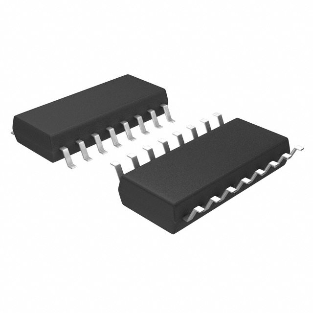
16 引脚、小尺寸封装 (SOP)
包装方法
塑料管
卷带和卷盘
www.fairchildsemi.com
FAN7621S — 适用于半桥谐振转换器的 PFM 控制器
2013 年 11 月
�Cr
V IN
VCC
VO
LVCC
Rmin
RT
Rmax
Rss
Css
AR
FAN7621S
HVCC
HO
CTR
LO
CS
SG PG
图 1. 典型应用电路(LLC 谐振半桥转换器)
框图
LVCC
12
Vre f
Vre f
1
IR T
IR T
2IR T
LV
3V
S
1V
R
CC
g o od
HVcc
In tern al
B ias
Vre f
Q
L U V+ / L U V-
H UV+ / H UV-
2V
RT
L evel
S h ifter
T im e
D elay
8
H ig h S id e
Gate D river
3 50n s
3
2
HO
CTR
D ivid er
AR
6
5k
B alan cin g
D elay
T im e
D elay
VC s s H/ VC s s L
L ow S id e
Gate D river
14
LO
3 50n s
S
LV
CC
R
g o od
S h utd own with o ut d elay
Q
TSD
L VC C
VO V P
VA O C P
D elay
50 n s
16
PG
10
SG
VO C P
D elay
1.5µs
-1
9
CS
图 2. 内部框图
© 2009 飞兆半导体公司
FAN7621S • Rev. 1.0.1
www.fairchildsemi.com
2
FAN7621S — 适用于半桥谐振转换器的 PFM 控制器
应用电路图
�FAN7621S — 适用于半桥谐振转换器的 PFM 控制器
引脚布局
(1 ) H V CC
P G (16 )
(2 ) C T R
N C (15 )
(3 ) H O
L O (14 )
(4 ) N C
N C (13 )
FAN7 6 21S
(5 ) N C
L V C C (12 )
(6 ) A R
N C (11 )
(7 ) N C
S G (10 )
(8 ) R T
CS
(9 )
图 3. 封装图
引脚定义
引脚号
名称
1
HVCC
这是高侧栅极驱动电路 IC 的电源电压。
2
CTR
这是低侧 MOSFET 的漏极。典型地,变压器连接到该引脚。
3
HO
这是高侧栅极驱动信号。
4
NC
无连接
5
NC
无连接
6
AR
此引脚用于在触发任何保护时对外部软启动电容放电。如果该引脚电压降至 0.2 V,所有保护
机制重新启动并且控制器重新开始工作。
7
NC
无连接
8
RT
该引脚用于编程开关频率。一般地,需要光耦连接到该引脚,用来调节输出电压的开关频率。
9
CS
此引脚检测流经低侧 MOSFET 的电流。典型地,负电压被施加到该引脚。
10
SG
该引脚为 控制地。
11
NC
无连接
12
LVCC
13
NC
无连接
14
LO
这是低侧栅极驱动信号。
15
NC
无连接
16
PG
该引脚为电源地。该引脚连接到低侧 MOSFET 的源极。
© 2009 飞兆半导体公司
FAN7621S • Rev. 1.0.1
说明
该引脚为控制 IC 的供电电压。
www.fairchildsemi.com
3
�应力超过绝对最大额定值,可能会损坏器件。在超出推荐的工作条件的情况下,该器件可能无法正常工作,所以不建议
让器件在这些条件下长期工作。此外,过度暴露在高于推荐的工作条件下,会影响器件的可靠性。绝对最大额定值仅是
应力规格值。TA=25C,除非另有说明。
符号
参数
最小值
最大值
VCTR-0.3
HVCC
单位
VHO
高侧栅极驱动电压
VLO
低侧栅极电压
-0.3
LVCC
LVCC
低侧电源电压
-0.3
25.0
V
-0.3
25.0
V
HVCC 至 VCTR 高侧 VCC 引脚至中点电压
V
VCTR
中点电压
-0.3
600.0
V
VAR
自动重启引脚输入电压
-0.3
LVCC
V
VCS
电流感测(CS)引脚输入电压
-5.0
1.0
V
VRT
RT 引脚输入电压
-0.3
5.0
V
50
V/ns
1.13
W
dVCTR/dt
容许中点电压压摆率
PD
总功耗
(1)
+150
最大结温
TJ
(1)
TSTG
推荐的工作结温
-40
+130
存储温度范围
-55
+150
C
C
注:
1. 所推荐的工作节温最大值受限于热保护功能。
热阻测试
符号
θJA
参数
节-环境之间热阻
© 2009 飞兆半导体公司
FAN7621S • Rev. 1.0.1
数值
单位
110
ºC/W
www.fairchildsemi.com
4
FAN7621S — 适用于半桥谐振转换器的 PFM 控制器
绝对最大额定值
�TA=25C,LVCC=17V,除非另有说明。
符号
参数
测试条件
最小值 典型值 最大值
单位
电源部分
ILK
偏置漏电流
HVCC=VCTR
50
μA
IQHVCC
HVCC 静态电源电流
(HVCCUV+) - 0.1V
50
120
μA
IQLVCC
LVCC 静态电源电流
(LVCCUV+) - 0.1V
100
200
μA
IOHVCC
工作 HVCC 电源电流(RMS值)
5
8
mA
100
200
μA
IOLVCC
工作 LVCC 电源电流(RMS值)
fOSC=100kHz, CLoad=1nF
6
9
mA
无开关
2
4
mA
fOSC=100kHz, CLoad=1nF
无开关
UVLO 部分
LVCCUV+
LVCC 电源欠压正向阈值(LVCC 启动)
11.2
12.5
13.8
V
LVCCUV-
LVCC 电源欠压负向阈值(LVCC 停止)
8.9
10.0
11.1
V
LVCCUVH
LVCC 电源欠压滞回
HVCCUV+
HVCC 电源欠压正向阈值(HVCC 启动)
8.2
9.2
10.2
V
HVCCUV-
HVCC 电源欠压负向阈值(HVCC 停止)
7.8
8.7
9.6
V
HVCCUVH
HVCC 电源欠压滞回
2.5
V
0.5
V
振荡器与反馈部分
VRT
V-I 转换器阈值电压
fOSC
输出振荡频率
DC
输出占空比
fSS
内部软启动初始频率
tSS
内部软启动时间
RT=5.2k
1.5
2.0
2.5
V
94
100
106
kHz
48
50
52
%
fSS=fOSC+40kHz, RT=5.2k
140
2
3
kHz
4
ms
输出部分
Isource
峰值源电流
HVCC=17V
250
360
mA
Isink
峰值灌电流
HVCC=17V
460
600
mA
65
ns
35
ns
tr
上升时间
tf
下降时间
VHOH
高电平的高侧栅极驱动信号 (VHVCC-VHO)
VHOL
低电平的高侧栅极驱动信号
VLOH
高电平的高侧栅极驱动信号 (VLVCC-VLO)
VLOL
低电平的高侧栅极驱动信号
© 2009 飞兆半导体公司
FAN7621S • Rev. 1.0.1
CLoad=1nF, HVCC=17V
IO=20mA
1.0
V
0.6
V
1.0
V
0.6
V
www.fairchildsemi.com
5
FAN7621S — 适用于半桥谐振转换器的 PFM 控制器
电气特性
�TA=25C,LVCC=17V,除非另有说明。
符号
参数
测试条件
最小值 典型值 最大值
单位
保护部分
VCssH
开始电压至放电 CSS
0.9
1.0
1.1
V
VCssL
充电 CSS 和复位保护的开始电压
0.16
0.20
0.24
V
VOVP
LVCC 过压保护
LVCC>21V
21
23
25
V
VAOCP
AOCP 阈值电压
V/t=-0.1V/µs
-1.0
-0.9
-0.8
V
tBAO
AOCP 消隐时间(2)
VOCP
OCP 阈值电压
tBO
OCP 消隐时间(2)
tDA
延迟时间(低侧)从 VAOCP 检测到关断(2)
TSD
热关闭温度(2)
VCS< VAOCP;
50
V/t=-0.1V/µs
V/t=-1V/µs
VCS< VOCP;
V/t=-1V/µs
ns
-0.64
-0.58
-0.52
V
1.0
1.5
2.0
μs
250
400
ns
130
150
C
V/t=-1V/µs
110
死区时间控制部分
DT
死区时间(3)
350
ns
注意:
2. 这些参数尽管得到保证,但未经过生产测试。
3. 这些参数尽管经过保证,也仅在 EDS(硅片测试)过程中测试。
© 2009 飞兆半导体公司
FAN7621S • Rev. 1.0.1
www.fairchildsemi.com
6
FAN7621S — 适用于半桥谐振转换器的 PFM 控制器
电气特性(续)
�1.1
1.1
1.05
1.05
Normalized at 25OC
Normalized at 25OC
这些测得的特性图在 TA=25ºC 下都被归一化。
1
0.95
1
0.95
0.9
0.9
-50
-25
0
25
50
75
-50
100
-25
0
Temp (OC)
50
75
100
图 5. 开关频率与温度的关系
1.1
1.1
1.05
1.05
Normalized at 25OC
Normalized at 25OC
图 4. 低侧 MOSFET 占空比与温度的关系
1
0.95
0.9
1
0.95
0.9
-50
-25
0
25
50
75
100
-50
-25
0
Temp (OC)
25
50
75
100
Temp (OC)
图 6. 高侧 VCC(HVCC) 启动与温度的关系
图 7. 高侧 VCC(HVCC) 停止与温度的关系
1.1
1.1
1.05
1.05
Normalized at 25OC
Normalized at 25OC
25
Temp (OC)
1
0.95
1
0.95
0.9
0.9
-50
-25
0
25
50
75
-50
100
-25
0
25
50
75
100
Temp (OC)
Temp (OC)
图 8. 低侧 VCC (LVCC) 启动与温度的关系
图 9. 低侧 VCC(LVCC) 停止与温度的关系
© 2009 飞兆半导体公司
FAN7621S • Rev. 1.0.1
www.fairchildsemi.com
7
FAN7621S — 适用于半桥谐振转换器的 PFM 控制器
典型性能特征
�1.1
1.1
1.05
1.05
Normalized at 25OC
Normalized at 25OC
这些测得的特性图在 TA=25ºC 下都被归一化。
1
0.95
0.9
1
0.95
0.9
-50
-25
0
25
50
75
100
-50
-25
0
Temp (OC)
50
Temp
75
100
(OC)
图 11. RT 电压与温度的关系
图 10. LVCC OVP 电压与温度的关系
1.1
1.05
1.05
Normalized at 25℃
1.1
Normalized at 25℃
25
1
0.95
1
0.95
0.9
0.9
-50
-25
0
25
50
75
100
-50
Temp(℃)
-25
0
25
50
75
100
Temp(℃)
图 12. VCssL 与温度的关系
图 13. VCssH 与温度的关系
1.1
Normalized at 25OC
1.05
1
0.95
0.9
-50
-25
0
25
50
75
100
Temp (OC)
图 14. OCP 电压与温度的关系
© 2009 飞兆半导体公司
FAN7621S • Rev. 1.0.1
www.fairchildsemi.com
8
FAN7621S — 适用于半桥谐振转换器的 PFM 控制器
典型性能特征(接上页)
�FAN7621S — 适用于半桥谐振转换器的 PFM 控制器
功能说明
1. 基本工作:FAN7621S 设计为驱动高侧和低侧
MOSFET,各占 50% 占空比。在连续转换间引入了固定
死区时间 350ns,如图 15 所示。
图 15. MOSFET 栅极驱动信号
2. 内部振荡器:FAN7621S 采用电流控制的振荡器,如图
16 所示。在内部,RT 引脚的电压调节在 2V,并且振荡器
电容 CT 的充电/放电电流通过使用电流镜像复制从 RT 引
脚 (ICTC) 流出的电流来获得。因此,开关频率随着 ICTC 的
增加而增加。
I CTC
V REF
I CTC
2I CTC
图 17. 谐振转换器典型增益曲线
+
3V
-
1V
+
CT
S
Q
R
-Q
F /F
-
+
-
RT
2V
C oun ter
( 1/4)
8
G ate d rive
图 18. 频率控制电路
图 16. 电流控制的振荡器
为了防止在启动阶段,冲击电流过大,输出电压过冲,需
要逐渐增加该谐振转换器的电压增益。由于谐振转换器的
电压增益与开关频率成反比,因此通过从初始高频率 (fISS)
向下扫描开关频率直至建立输出电压,来实施软启动。通
过在 RT 引脚上连接 R-C 串联网络来建立软启动电路,如
图 18 所示。FAN7621S 也有一个 3ms 的内部软启动来降
低初始周期过程中的电流过冲,这就向外部软启动电路的
初始频率中增加了 40kHz,如图 19 所示。软启动的初始
频率由下式给出:
3. 频率设置:图 17 显示谐振转换器的典型电压增益曲
线,其中增益与 ZVS 区中的开关频率成反比。输出电压
可通过调制开关频率来调节。图 18 显示 RT 引脚的典型电
路配置,其中光电耦合器电阻连接至 RT 引脚以调制开关
频率。
最小开关频率由下式确定:
f min
5.2k
100( kHz )
Rmin
(1)
f ISS (
假定光耦晶体管的饱和电压为 0.2V,则最大开关频率决定
于:
f max (
5.2k 4.68k
) 100(kHz )
Rmin
Rmax
© 2009 飞兆半导体公司
FAN7621S • Rev. 1.0.1
5.2k 5.2k
) 100 40 ( kHz )
Rmin
RSS
(3)
通常将初始(软启动)频率设置为谐振网络的谐振频率
(fO) 的两至三倍。
(2)
www.fairchildsemi.com
9
�t SS R SS CSS
(a )
(b )
( a)
(b ) (a )
(b )
L V CC
(4)
V AR
V CssH
V CssL
fs
f
ISS
ICr
40kHz
Control loop
take over
t stop
tS /S
(a ) P r o te ction s a r e tr igge r e d, ( b ) F S F R- U S r e sta r ts
图 21. 自动重启操作
time
5. 保护电路:FAN7621S 具有多个自我保护功能,如过流
保护 (OLP)、异常过流保护 (OCP)、过压保护 (OVP) 和热
关断 (TSD)。这些保护为自动重启模式保护,如图 21 所
示。
图 19. 软启动的频率扫描
4. 自重启:即使外部电源电压触发内置保护,FAN7621S
也可自动重启。如图 20 和图 21 所示;一旦触发任何保
护,M1 开关即导通并且禁用V-I转换器。CSS 开始放电,
直至 CSS 上的 VCss 降至 VCssL。然后所有保护复位,M1
关断,并且 V-I 转换器恢复。FAN7621S 再次通过软启动
开始开关操作。如果在 VCss 处于 VCssL 和 VCssH 电平以下
时触发保护,将立即终止开关操作,VCss 继续增大直至达
到 VCssH,然后 CSS 被 M1 放电。
一旦检测到故障情况,开关操作即终止并且 MOSFET 保
持关断。当 LVCC 降至 10V 的 LVCC 停止电压或 AR 信号
为高电平时,将复位保护。当 LVCC 达到 12.5V 的启动电
压时,FAN7621S 恢复正常操作。
图 22. 保护框图
5.1 过流保护 (OCP):当感测引脚电压降至低于 -0.58V
时,触发 OCP 并且 MOSFET 保持关断。此保护具有
1.5µs 的关断时间延迟以避免启动期间提前关断。
5.2 异常过流保护 (AOCP):如果次级整流器二极管短
路,具有极高 di/dt 的大电流可在触发 OCP 之前流经
MOSFET。当感测引脚电压降至低于 -0.9V 时,将触发
AOCP,且没有关断延迟。
图 20. AR 引脚的内部框图
触发保护后,FAN7621S 在停止时间 tstop 期内被禁用,其
中 VCss 下降并达到 VCssL。FAN7621S 的停止时间可由下
式估算得出:
tstop =Css · Rss +Rmin ||5kΩ
5.3 过压保护 (OVP):当 LVCC 达到 23V 时,OVP 触
发。当变压器的辅助绕组向控制器供应 VCC 时,使用此
保护。
(5)
5.4 热关断 (TSD):如果结温超过约 130C,将触发热
关断。
对于软启动时间,ts/s 可设置为等式 (4)。
© 2009 飞兆半导体公司
FAN7621S • Rev. 1.0.1
www.fairchildsemi.com
10
FAN7621S — 适用于半桥谐振转换器的 PFM 控制器
软启动时间是 RC 时间常数的三至四倍。RC 时间常数如
下所示:
�图 23. 半波检测
图 24. 全波检测
图 25. 占空比平衡示例
© 2009 飞兆半导体公司
FAN7621S • Rev. 1.0.1
www.fairchildsemi.com
11
FAN7621S — 适用于半桥谐振转换器的 PFM 控制器
7. PCB 布局指南:由于主变压器的辐射噪音、主变压器
的次级端漏感不相等等原因可能发生占空比不平衡问题。
RT 引脚附近的控制元件在 PCB 布局上被主初级端电流环
路包围是造成占空比不平衡的主要原因。当高低侧
MOSFET 交替导通时,由初级端电流导致的元件上磁场
的方向发生变化。相互方向相反的磁场产生通过、进入或
从 RT 引脚流出的电流,这使得每个 MOSFET 的导通持续
时间各不相同。强烈建议将 RT 引脚附近的控制元件与
PCB 布局上的初级端电流路径分开。图 25 显示占空比平
衡情况的示例。黄色和蓝色行分别显示下端和上端
MOSFET 导通时的初级端电流。初级端电流不包围控制
器的任何元件。
6. 使用电阻的电流感测:FAN7621S 检测漏电流为负压,
如图 23 和图 24 所示。半波检测方式允许检测电阻产生低
功耗,但是全波检测方式的检测信号具有较低开关噪声。
�10.30
10.10
-A-
0.47 TYP
16
9
16 15
10 9
5.01 TYP
5.40
5.20 -B-
7.8
9.27 TYP
1
2
7
8
3.9
1
0.2 C B A
ALL LEAD TIPS
8
1.27
TYP
PIN #1 IDENT.
ALL LEAD TIPS
0.1 C
0.60 TYP
SEE DETAIL A
0.16 1.90
0.14 1.70
2.1 MAX
0.25
0.15
0.51
0.35
1.27 TYP
0.12
7° TYP
GAGE PLANE
0-8° TYP
MIN
0.25
(2.13 TYP)
0.25
SEATING PLANE
1.25
C A
NOTES:
A. CONFORMS TO EIAJ EDR-7320
REGISTRATION, ESTABLISHED IN
DECEMBER, 1998.
B. DIMENSIONS ARE IN MILLIMETERS.
C. DIMENSIONS ARE EXCLUSIVE OF BURRS,
MOLD FLASH, AND TIE BAR EXTRUSIONS.
D. DRAWING FILENAME: MKT-M16Drev5
�ON Semiconductor and
are trademarks of Semiconductor Components Industries, LLC dba ON Semiconductor or its subsidiaries in the United States and/or other countries.
ON Semiconductor owns the rights to a number of patents, trademarks, copyrights, trade secrets, and other intellectual property. A listing of ON Semiconductor’s product/patent
coverage may be accessed at www.onsemi.com/site/pdf/Patent−Marking.pdf. ON Semiconductor reserves the right to make changes without further notice to any products herein.
ON Semiconductor makes no warranty, representation or guarantee regarding the suitability of its products for any particular purpose, nor does ON Semiconductor assume any liability
arising out of the application or use of any product or circuit, and specifically disclaims any and all liability, including without limitation special, consequential or incidental damages.
Buyer is responsible for its products and applications using ON Semiconductor products, including compliance with all laws, regulations and safety requirements or standards,
regardless of any support or applications information provided by ON Semiconductor. “Typical” parameters which may be provided in ON Semiconductor data sheets and/or
specifications can and do vary in different applications and actual performance may vary over time. All operating parameters, including “Typicals” must be validated for each customer
application by customer’s technical experts. ON Semiconductor does not convey any license under its patent rights nor the rights of others. ON Semiconductor products are not
designed, intended, or authorized for use as a critical component in life support systems or any FDA Class 3 medical devices or medical devices with a same or similar classification
in a foreign jurisdiction or any devices intended for implantation in the human body. Should Buyer purchase or use ON Semiconductor products for any such unintended or unauthorized
application, Buyer shall indemnify and hold ON Semiconductor and its officers, employees, subsidiaries, affiliates, and distributors harmless against all claims, costs, damages, and
expenses, and reasonable attorney fees arising out of, directly or indirectly, any claim of personal injury or death associated with such unintended or unauthorized use, even if such
claim alleges that ON Semiconductor was negligent regarding the design or manufacture of the part. ON Semiconductor is an Equal Opportunity/Affirmative Action Employer. This
literature is subject to all applicable copyright laws and is not for resale in any manner.
PUBLICATION ORDERING INFORMATION
LITERATURE FULFILLMENT:
Literature Distribution Center for ON Semiconductor
19521 E. 32nd Pkwy, Aurora, Colorado 80011 USA
Phone: 303−675−2175 or 800−344−3860 Toll Free USA/Canada
Fax: 303−675−2176 or 800−344−3867 Toll Free USA/Canada
Email: orderlit@onsemi.com
© Semiconductor Components Industries, LLC
N. American Technical Support: 800−282−9855 Toll Free
USA/Canada
Europe, Middle East and Africa Technical Support:
Phone: 421 33 790 2910
Japan Customer Focus Center
Phone: 81−3−5817−1050
www.onsemi.com
1
ON Semiconductor Website: www.onsemi.com
Order Literature: http://www.onsemi.com/orderlit
For additional information, please contact your local
Sales Representative
www.onsemi.com
�


 工商网监
湘ICP备2023018690号
工商网监
湘ICP备2023018690号
