FDMD8630
MOSFET – N-Channel,
POWERTRENCH), Dual
30 V, 167 A, 1.0 mW
General Description
This package integrates two N−Channel devices connected
internally in common−source configuration. This enables very low
package parasitics and optimized thermal path to the common source
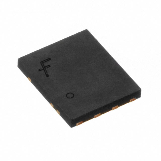
pad on the bottom. Provides a very small footprint (5 x 6 mm) for
higher power density.
www.onsemi.com
Top
Bottom
Pin 1
G1
Features
•
•
•
•
•
•
•
D1
D1
S1 / S2
Common Source Configuration to Eliminate PCB Routing
Large Source Pad on Bottom of Package for Enhanced Thermals
Max rDS(on) = 1.0 mW at VGS = 10 V, ID = 38 A
Max rDS(on) = 1.3 mW at VGS = 4.5 V, ID = 33 A
Ideal for Flexible Layout in Secondary Side Synchronous
Rectification
100% UIL Tested
This Device is Pb−Free and is RoHS Compliant
D2
D2
D2
D1
G2
PQFN8 5X6, 1.27P
CASE 483AS
MARKING DIAGRAM
$Y&Z&3&K
Applications
FDMD
• Isolated DC−DC Synchronous Rectifiers
• Common Ground Load Switches
8630
&Y
&Z
&3
&K
FDMD8630
= ON Semiconductor Logo
= Assembly Plant Code
= Numeric Date Code
= Lot Code
= Specific Device Code
PIN CONFIGURATION
G1
1
8
D2
D1
2
7
D2
D1
3
6
D2
D1
4
5
G2
S1,S2 to backside
ORDERING INFORMATION
See detailed ordering and shipping information on page 2 of
this data sheet.
© Semiconductor Components Industries, LLC, 2017
July, 2019 − Rev. 2
1
Publication Order Number:
FDMS3604S/D
�FDMD8630
MOSFET MAXIMUM RATINGS TA = 25°C Unless Otherwise Noted
Parameter
Symbol
Ratings
Units
VDS
Drain to Source Voltage
30
V
VGS
Gate to Source Voltage
±20
V
Drain Current
−Continuous − TC = 25°C (Note 5)
167
−Continuous − TC =100°C (Note 5)
106
−Continuous − TA = 25°C (Note 1a)
38
ID
EAS
PD
TJ, TSTG
A
−Pulsed − (Note 4)
1178
Single Pulse Avalanche Energy (Note 3)
726
mJ
Power Dissipation for Single Operation TC = 25 °C
43
W
Power Dissipation for Single Operation TA = 25 °C (Note 1a)
2.3
Operating and Storage Junction Temperature Range
−55 to +150
°C
Ratings
Unit
°C/W
THERMAL CHARACTERISTICS
Symbol
Parameter
RθJC
Thermal Resistance, Junction to Case
2.9
RθJA
Thermal Resistance, Junction to Ambient (Note 1a)
55
PACKAGE MARKING AND ORDERING INFORMATION
Device Marking
Device
Package
Reel Size
Tape Width
Quantity
FDMD8630
FDMD8630
Power 5 x 6
13”
12 mm
3000 Units
ELECTRICAL CHARACTERISTICS TJ = 25°C Unless Otherwise Noted
Parameter
Symbol
Test Conditions
Min
Typ
Max
Units
OFF CHARACTERISTICS
BVDSS
Drain to Source Breakdown Voltage
ID = 250 mA, VGS = 0 V
30
V
DBVDSS /
DTJ
Breakdown Voltage Temperature
Coefficient
ID = 250 mA, referenced to 25°C
IDSS
Zero Gate Voltage Drain Current
VDS = 24 V, VGS = 0 V
1
mA
IGSS
Gate to Source Leakage Current,
Forward
VGS = 20 V, VDS= 0 V
100
nA
3.0
V
15
mV/°C
ON CHARACTERISTICS
VGS(th)
Gate to Source Threshold Voltage
VGS = VDS, ID = 250 mA
DVGS(th) /
DTJ
Gate to Source Threshold Voltage
Temperature Coefficient
ID = 250 mA, referenced to 25°C
−6
Static Drain to Source On Resistance
VGS = 10 V, ID = 38 A
0.6
1.0
VGS = 4.5 V, ID = 33 A
0.8
1.3
VGS = 4.5 V, ID = 33 A, TJ = 125°C
0.9
1.5
VDD = 5 V, ID = 38 A
281
VDS = 15 V, VGS = 0 V, f = 1 MHz
rDS(on)
gFS
Forward Transconductance
1.0
1.6
mV/°C
mW
S
DYNAMIC CHARACTERISTICS
Ciss
Input Capacitance
7090
9930
pF
Coss
Output Capacitance
2025
2835
pF
Crss
Reverse Transfer Capacitance
212
300
pF
1.9
3.8
W
Rg
Gate Resistance
0.1
SWITCHING CHARACTERISTICS
www.onsemi.com
2
�FDMD8630
ELECTRICAL CHARACTERISTICS TJ = 25°C Unless Otherwise Noted (continued)
Parameter
Symbol
Test Conditions
Min
Typ
Max
Units
14
26
ns
SWITCHING CHARACTERISTICS
td(on)
tr
td(off)
tf
VDD = 15 V, ID = 38 A
VGS = 10 V, RGEN = 6 W
Turn−On Delay Time
Rise Time
15
27
ns
Turn−Off Delay Time
66
105
ns
Fall Time
24
39
ns
97
142
nC
46
74
nC
Qg(TOT)
Total Gate Charge
VGS = 0 V to 10 V
Qg(TOT)
Total Gate Charge
VGS = 0 V to 4.5 V
VDD = 15 V
ID = 38 A
Qgs
Gate to Source Gate Charge
17
nC
Qgd
Gate to Drain “Miller” Charge
12
nC
DRAIN−SOURCE DIODE CHARACTERISTICS
VSD
Source to Drain Diode Forward Voltage
VGS = 0 V, IS = 38 A (Note 2)
0.8
VSD
1.3
V
Source to Drain Diode Forward Voltage
VGS = 0 V, IS = 2 A (Note 2)
0.7
1.2
V
trr
Reverse Recovery Time
IF = 38 A, di/dt = 100 A/ms
64
103
ns
Qrr
Reverse Recovery Charge
56
90
nC
1. RqJA is determined with the device mounted on a 1 in2 pad 2 oz copper pad on a 1.5 x 1.5 in. board of FR−4 material. RqJA is guaranteed
by design while RqCA is determined by the user’s board design.
b. 125°C/W when mounted on
a minimum pad of 2 oz copper
a. 55°C/W when mounted on
a 1 in2 padof 2 oz copper
SS
SF
DS
DF
G
SS
SF
DS
DF
G
2.
3.
4.
5.
Pulse Test: Pulse Width < 300 ms, Duty cycle < 2.0%.
EAS of 726 mJ is based on starting TJ = 25°C, L = 3 mH, IAS = 22 A, VDD = 30 V, VGS = 10 V. 100% tested at L = 0.1 mH, IAS = 70 A.
Pulsed Id please refer to Fig 11 SOA graph for more details.
Computed continuous current limited to Max Junction Temperature only, actual continuous current will be limited by thermal &
electro−mechanical application board design.
www.onsemi.com
3
�FDMD8630
TYPICAL CHARACTERISTICS
TJ = 25°C Unless Otherwise Noted
200
ID, DRAIN CURRENT (A)
VGS = 4.5 V
VGS = 4 V
150
VGS = 3.5 V
100
VGS = 3 V
50
PULSE DURATION = 80 ms
DUTY CYCLE = 0.5% MAX
0
0.0
0.2
0.4
0.6
VDS, DRAIN TO SOURCE VOLTAGE (V)
rDS(on), DRAIN TO
1.1
1.0
0.9
0.8
-25
0
25
50 75 100
TJ, JUNCTION TEMPERATURE ( oC)
125
SOURCE ON−RESISTANCE (mW)
NORMALIZED
DRAIN TO SOURCE ON− RESISTANCE
1.2
80
120
160
200
120
TJ = 150 o C
80
TJ = 25oC
40
TJ = -55 oC
2
3
PULSE DURATION = 80 ms
DUTY CYCLE = 0.5% MAX
4
TJ = 25 o C
2
2
4
TJ = 125 oC
6
8
10
Figure 4. On−Resistance vs Gate to Source
Voltage
IS, REVERSE DRAIN CURRENT (A)
ID, DRAIN CURRENT (A)
40
VGS, GATE TO SOURCE VOLTAGE (V)
VDS = 5 V
1
0
6
0
PULSE DURATION = 80 ms
DUTY CYCLE = 0.5% MAX
0
0
VGS = 4 V VGS = 4.5 V VGS = 10 V
ID = 38 A
150
200
0
1
8
Figure 3. Normalized On Resistance
vs Junction Temperature
160
VGS = 3.5 V
2
10
1.3
-50
3
Figure 2. Normalized On−Resistance vs Drain
Current and Gate Voltage
1.4
0.7
-75
VGS = 3 V
4
ID , DRAIN CURRENT (A)
ID = 38 A
VGS = 10 V
1.5
PULSE DURATION = 80 ms
DUTY CYCLE = 0.5% MAX
5
0.8
Figure 1. On−Region Characteristics
1.6
6
NORMALIZED
DRAIN TO SOURCE ON− RESISTANCE
VGS = 10 V
200
100
10
TJ = 150 oC
1
TJ = 25oC
0.1
TJ = -55 o C
0.01
0.001
0.0
4
VGS = 0 V
VGS, GATE TO SOURCE VOLTAGE (V)
0.2
0.4
0.6
0.8
1.0
VSD, BODY DIODE FORWARD VOLTAGE (V)
Figure 5. Transfer Characteristics
Figure 6. Source to Drain Diode
Forward Voltage vs Source Current
www.onsemi.com
4
1.2
�FDMD8630
TYPICAL CHARACTERISTICS
TJ = 25°C Unless Otherwise Noted (continued)
10
10000
VGS, GATE TO SOURCE VOLTAGE (V)
ID = 38 A
C iss
8
CAPACITANCE (pF)
VDD = 15 V
6
VDD = 10 V
VDD = 20 V
4
2
0
0
20
40
60
80
C oss
1000
f = 1 MHz
VGS = 0 V
100
10
30
Figure 8. Capacitance vs Drain to Source Voltage
Figure 7. Gate Charge Characteristics
200
100
160
ID, DRAIN CURRENT (A)
IAS, AVALANCHE CURRENT (A)
1
VDS, DRAIN TO SOURCE VOLTAGE (V)
Qg, GATE CHARGE (nC)
TJ = 25 oC
TJ = 125oC
0.1
1
10
VGS = 10 V
120
TJ = 100 oC
10
1
0.01
100
80
VGS = 4.5 V
40
0
25
1000
RqJC = 2.9 o C/W
tAV, TIME IN AVALANCHE (ms)
0.01
0.01
P(PK), PEAK TRANSIENT POWER (W)
10ms
100
0.1
100
125
150
o C)
100000
1000
1
75
Figure 10. Maximum Continuous Drain Current
vs Case Temperature
3000
10
50
T , CASE TEMPERATURE (
Figure 9. Unclamped Inductive Switching
Capability
ID, DRAIN CURRENT (A)
C rss
100
0.1
100 ms
THIS AREA IS
LIMITED BYrDS(on)
SINGLE PULSE
TJ = MAX RATED
RqJC = 2.9 oC/W
TC = 25 oC
0.1
1 ms
10 ms
100 ms
CURVE BENT TO
MEASURED DATA
1
10
100 200
SINGLE PULSE
RqJC= 2.9 oC/W
10000
TC = 25 oC
1000
100
10
−5
10
VDS, DRAIN to SOURCE VOLTAGE (V)
10
−4
10
−3
10
−2
10
−1
1
t, PULSE WIDTH (sec)
Figure 11. Forward Bias Safe Operating Area
Figure 12. Single Pulse Maximum Power
Dissipation
www.onsemi.com
5
�FDMD8630
TYPICAL CHARACTERISTICS
TJ = 25°C Unless Otherwise Noted (continued)
r(t), NORMALIZED EFFECTIVE TRANSIENT
THERMAL RESISTANCE
2
1
0.1
DUTY CYCLE−DESCENDING ORDER
D = 0.5
0.2
0.1
0.05
0.02
0.01
P DM
t1
t2
NOTES:
0.01
0.001
−5
10
ZqJC (t) = r(t) x R qJC
R qJC = 2.9 oC/W
Peak TJ = PDM x Z qJC (t) + TC
Duty Cycle, D = t1 / t2
SINGLE PULSE
10
−4
10
−3
10
−2
10
−1
1
t, RECTANGULAR PULSE DURATION (sec)
Figure 13. Junction−to−Ambient Transient Thermal Response Curve
POWERTRENCH is registered trademark of Semiconductor Components Industries, LLC (SCILLC) or its subsidiaries in the United States and/or other
countries.
www.onsemi.com
6
�MECHANICAL CASE OUTLINE
PACKAGE DIMENSIONS
PQFN8 5X6, 1.27P
CASE 483AS
ISSUE A
DOCUMENT NUMBER:
DESCRIPTION:
98AON13667G
PQFN8 5X6, 1.27P
DATE 17 MAY 2021
Electronic versions are uncontrolled except when accessed directly from the Document Repository.
Printed versions are uncontrolled except when stamped “CONTROLLED COPY” in red.
PAGE 1 OF 1
ON Semiconductor and
are trademarks of Semiconductor Components Industries, LLC dba ON Semiconductor or its subsidiaries in the United States and/or other countries.
ON Semiconductor reserves the right to make changes without further notice to any products herein. ON Semiconductor makes no warranty, representation or guarantee regarding
the suitability of its products for any particular purpose, nor does ON Semiconductor assume any liability arising out of the application or use of any product or circuit, and specifically
disclaims any and all liability, including without limitation special, consequential or incidental damages. ON Semiconductor does not convey any license under its patent rights nor the
rights of others.
© Semiconductor Components Industries, LLC, 2019
www.onsemi.com
�onsemi,
, and other names, marks, and brands are registered and/or common law trademarks of Semiconductor Components Industries, LLC dba “onsemi” or its affiliates
and/or subsidiaries in the United States and/or other countries. onsemi owns the rights to a number of patents, trademarks, copyrights, trade secrets, and other intellectual property.
A listing of onsemi’s product/patent coverage may be accessed at www.onsemi.com/site/pdf/Patent−Marking.pdf. onsemi reserves the right to make changes at any time to any
products or information herein, without notice. The information herein is provided “as−is” and onsemi makes no warranty, representation or guarantee regarding the accuracy of the
information, product features, availability, functionality, or suitability of its products for any particular purpose, nor does onsemi assume any liability arising out of the application or use
of any product or circuit, and specifically disclaims any and all liability, including without limitation special, consequential or incidental damages. Buyer is responsible for its products
and applications using onsemi products, including compliance with all laws, regulations and safety requirements or standards, regardless of any support or applications information
provided by onsemi. “Typical” parameters which may be provided in onsemi data sheets and/or specifications can and do vary in different applications and actual performance may
vary over time. All operating parameters, including “Typicals” must be validated for each customer application by customer’s technical experts. onsemi does not convey any license
under any of its intellectual property rights nor the rights of others. onsemi products are not designed, intended, or authorized for use as a critical component in life support systems
or any FDA Class 3 medical devices or medical devices with a same or similar classification in a foreign jurisdiction or any devices intended for implantation in the human body. Should
Buyer purchase or use onsemi products for any such unintended or unauthorized application, Buyer shall indemnify and hold onsemi and its officers, employees, subsidiaries, affiliates,
and distributors harmless against all claims, costs, damages, and expenses, and reasonable attorney fees arising out of, directly or indirectly, any claim of personal injury or death
associated with such unintended or unauthorized use, even if such claim alleges that onsemi was negligent regarding the design or manufacture of the part. onsemi is an Equal
Opportunity/Affirmative Action Employer. This literature is subject to all applicable copyright laws and is not for resale in any manner.
PUBLICATION ORDERING INFORMATION
LITERATURE FULFILLMENT:
Email Requests to: orderlit@onsemi.com
onsemi Website: www.onsemi.com
◊
TECHNICAL SUPPORT
North American Technical Support:
Voice Mail: 1 800−282−9855 Toll Free USA/Canada
Phone: 011 421 33 790 2910
Europe, Middle East and Africa Technical Support:
Phone: 00421 33 790 2910
For additional information, please contact your local Sales Representative
�