ON Semiconductor
Is Now
To learn more about onsemi™, please visit our website at
www.onsemi.com
onsemi and and other names, marks, and brands are registered and/or common law trademarks of Semiconductor Components Industries, LLC dba “onsemi” or its affiliates and/or
subsidiaries in the United States and/or other countries. onsemi owns the rights to a number of patents, trademarks, copyrights, trade secrets, and other intellectual property. A listing of onsemi
product/patent coverage may be accessed at www.onsemi.com/site/pdf/Patent-Marking.pdf. onsemi reserves the right to make changes at any time to any products or information herein, without
notice. The information herein is provided “as-is” and onsemi makes no warranty, representation or guarantee regarding the accuracy of the information, product features, availability, functionality,
or suitability of its products for any particular purpose, nor does onsemi assume any liability arising out of the application or use of any product or circuit, and specifically disclaims any and all
liability, including without limitation special, consequential or incidental damages. Buyer is responsible for its products and applications using onsemi products, including compliance with all laws,
regulations and safety requirements or standards, regardless of any support or applications information provided by onsemi. “Typical” parameters which may be provided in onsemi data sheets and/
or specifications can and do vary in different applications and actual performance may vary over time. All operating parameters, including “Typicals” must be validated for each customer application
by customer’s technical experts. onsemi does not convey any license under any of its intellectual property rights nor the rights of others. onsemi products are not designed, intended, or authorized
for use as a critical component in life support systems or any FDA Class 3 medical devices or medical devices with a same or similar classification in a foreign jurisdiction or any devices intended for
implantation in the human body. Should Buyer purchase or use onsemi products for any such unintended or unauthorized application, Buyer shall indemnify and hold onsemi and its officers, employees,
subsidiaries, affiliates, and distributors harmless against all claims, costs, damages, and expenses, and reasonable attorney fees arising out of, directly or indirectly, any claim of personal injury or death
associated with such unintended or unauthorized use, even if such claim alleges that onsemi was negligent regarding the design or manufacture of the part. onsemi is an Equal Opportunity/Affirmative
Action Employer. This literature is subject to all applicable copyright laws and is not for resale in any manner. Other names and brands may be claimed as the property of others.
�1200 V, 15 A NPT Trench IGBT
Features
• NPT Trench Technology, Positive temperature coefficient
• Low Saturation Voltage: VCE(sat), typ = 1.9 V
@ IC = 15 A and TC = 25C
Description
Using ON Semiconductor's proprietary trench design and
advanced NPT technology, the 1200V NPT IGBT offers
superior conduction and switching performances, high
avalanche ruggedness and easy parallel operation.
This device is well suited for the resonant or soft switching application such as induction heating, microwave oven.
• Low Switching Loss: Eoff, typ = 0.6 mJ
@ IC = 15 A and TC = 25C
• Extremely Enhanced Avalanche Capability
C
G
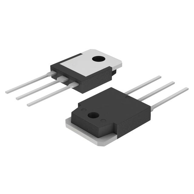
TO-3P
E
G C E
Absolute Maximum Ratings
Symbol
Description
Ratings
Unit
VCES
Collector-Emitter Voltage
1200
V
VGES
Gate-Emitter Voltage
20
V
IC
Collector Current
@ TC = 25C
30
A
Collector Current
@ TC = 100C
15
A
45
A
30
A
ICM
IF
IFM
PD
Pulsed Collector Current
(Note 1)
Diode Continuous Forward Current
@ TC = 25C
Diode Continuous Forward Current
@ TC = 100C
Diode Maximum Forward Current
15
A
45
A
Maximum Power Dissipation
@ TC = 25C
186
W
Maximum Power Dissipation
@ TC = 100C
74
W
TJ
Operating Junction Temperature
-55 to +150
C
Tstg
Storage Temperature Range
-55 to +150
C
TL
Maximum Lead Temp. for soldering
Purposes, 1/8” from case for 5 seconds
300
C
Thermal Characteristics
Typ.
Max.
Unit
RJC
Symbol
Thermal Resistance, Junction-to-Case for IGBT
Parameter
--
0.67
C/W
RJC
Thermal Resistance, Junction-to-Case for Diode
--
2.88
C/W
RJA
Thermal Resistance, Junction-to-Ambient
--
40
C/W
Notes:
(1) Repetitive rating: Pulse width limited by max. junction temperature
©2006 Semiconductor Components Industries, LLC.
October-2017,Rev.3
Publication Order Number:
FGA15N120ANTDTU/D
FGA15N120ANTDTU — 1200 V, 15 A NPT Trench IGBT
FGA15N120ANTDTU
�Part Number
Top Mark
Package
Packing
Method
FGA15N120ANTDTU-F109
FGA15N120ANTDTU
TO-3P
Tube
Electrical Characteristics of the IGBT
Symbol
Parameter
Reel Size Tape Width Quantity
N/A
N/A
30
TC = 25°C unless otherwise noted
Test Conditions
Min.
Typ.
Max.
Unit
Off Characteristics
ICES
Collector Cut-Off Current
VCE = VCES, VGE = 0 V
--
--
3
mA
IGES
G-E Leakage Current
VGE = VGES, VCE = 0 V
--
--
± 250
nA
On Characteristics
VGE(th)
G-E Threshold Voltage
IC = 15 mA, VCE = VGE
VCE(sat)
Collector to Emitter
Saturation Voltage
IC = 15 A,
4.5
6.5
8.5
V
VGE = 15 V
--
1.9
2.4
V
IC = 15 A, VGE = 15 V,
TC = 125C
--
2.2
--
V
IC = 30 A,
--
2.3
--
V
--
2650
--
pF
--
143
--
pF
--
96
--
pF
VGE = 15 V
Dynamic Characteristics
Cies
Input Capacitance
Coes
Output Capacitance
Cres
Reverse Transfer Capacitance
VCE = 30 V, VGE = 0 V,
f = 1 MHz
Switching Characteristics
td(on)
Turn-On Delay Time
tr
Rise Time
td(off)
Turn-Off Delay Time
tf
Fall Time
Eon
Turn-On Switching Loss
Eoff
Turn-Off Switching Loss
Ets
Total Switching Loss
td(on)
Turn-On Delay Time
tr
Rise Time
td(off)
Turn-Off Delay Time
VCC = 600 V, IC = 15 A,
RG = 10 , VGE = 15 V,
Inductive Load, TC = 25C
VCC = 600 V, IC = 15 A,
RG = 10 , VGE = 15 V,
Inductive Load, TC = 125C
--
15
--
ns
--
20
--
ns
--
160
--
ns
--
100
180
ns
--
3
4.5
mJ
--
0.6
0.9
mJ
--
3.6
5.4
mJ
--
15
--
ns
--
20
--
ns
--
170
--
ns
tf
Fall Time
--
150
--
ns
Eon
Turn-On Switching Loss
--
3.2
4.8
mJ
Eoff
Turn-Off Switching Loss
--
0.8
1.2
mJ
Ets
Total Switching Loss
--
4.0
6.0
mJ
Qg
Total Gate Charge
Qge
Gate-Emitter Charge
Qgc
Gate-Collector Charge
VCE = 600 V, IC = 15 A,
VGE = 15 V
www.onsemi.com
2
--
120
180
nC
--
16
22
nC
--
50
65
nC
FGA15N120ANTDTU — 1200 V, 15 A NPT Trench IGBT
Package Marking and Ordering Information
�C
Symbol
Parameter
= 25°C unless otherwise noted
Test Conditions
Min.
Typ.
Max.
Unit
1.7
2.7
V
VFM
Diode Forward Voltage
IF = 15 A
TC = 25C
--
TC = 125C
--
1.8
--
trr
Diode Reverse Recovery Time
IF = 15 A
diF/dt = 200 A/s
TC = 25C
--
210
330
TC = 125C
--
280
--
Irr
Diode Peak Reverse Recovery Current
TC = 25C
--
27
40
TC = 125C
--
31
--
Qrr
Diode Reverse Recovery Charge
TC = 25C
--
2835
6600
TC = 125C
--
4340
--
www.onsemi.com
3
ns
A
nC
FGA15N120ANTDTU — 1200 V, 15 A NPT Trench IGBT
Electrical Characteristics of DIODE T
�Figure 1. Typical Output Characteristics
200
150
o
T C = 25 C
Common Emitter
VGE = 15V
20V
17V
15V
o
12V
TC = 25 C
120
o
150
Collector Current , IC [A]
Collector Current, IC [A]
Figure 2. Typical Saturation Voltage
Characteristics
V GE = 10V
100
50
TC = 125 C
90
60
30
0
0
2
4
6
8
0
10
0
2
Collector-Emitter Voltage, V CE [V]
Figure 3. Saturation Voltage vs. Case
Temperature at Variant Current Level
Common Emitter
V GE = 15V
Common Emitter
o
T C = 25 C
16
IC = 24A
2.5
IC = 15A
2.0
12
8
4
24A
50
75
100
125
0
150
4
Case Temperature, TC [ C]
Figure 5. Saturation Voltage vs. VGE
12
16
20
Figure 6. Capacitance Characteristics
3500
Common Emitter
o
TC = 125 C
3000
Ciss
2500
12
Capacitance [pF]
Collector-Emitter Voltage, VCE [V]
8
Gate-Emitter Voltage, V GE [V]
o
16
15A
I C = 7.5A
0
1.5
25
6
Figure 4. Saturation Voltage vs. VGE
Collector-Emitter Voltage, VCE [V]
Collector-Emitter Voltage, VCE [V]
3.0
4
Collector-Emitter Voltage, VCE [V]
8
4
24A
15A
2000
o
0
4
8
T C = 25 C
1000
Coss
500
IC = 7.5A
0
Common Emitter
VGE = 0V, f = 1MHz
1500
Crss
0
12
16
0.1
20
1
10
Collector-Emitter Voltage, VCE[V]
Gate-Emitter Voltage, V GE [V]
www.onsemi.com
4
FGA15N120ANTDTU — 1200 V, 15 A NPT Trench IGBT
Typical Performance Characteristics
�(Continued)
Figure 7. Turn-On Characteristics vs. Gate
Resistance
Figure 8. Turn-Off Characteristics vs. Gate
Resistance
100
Common Emitter
V CC = 600V, V GE = 15V
IC = 15A
1000
td(off)
o
T C = 25 C
10
o
T C = 125 C
Switching Time [ns]
Switching Time [ns]
tr
td(on)
Common Emitter
V CC = 600V, V GE = 15V
100
tf
IC = 15A
o
T C = 25 C
o
T C = 125 C
10
1
0
0
10
20
30
40
50
60
10
20
70
Gate Resistance, RG[ ]
Figure 9. Switching Loss vs. Gate Resistance
50
60
70
Common Emitter
V GE = 15V, R G = 10
o
T C = 25 C
100
IC = 15A
o
T C = 125 C
o
T C = 25 C
Switching Time [ns]
o
Switching Loss [mJ]
40
Figure 10. Turn-On Characteristics vs.
Collector Current
Common Emitter
V CC = 600V, V GE = 15V
10
30
Gate Resistance, R G [ ]
T C = 125 C
Eon
Eoff
tr
td(on)
10
1
0
10
20
30
40
50
60
10
70
15
Gate Resistance, R G [ ]
Figure 11. Turn-Off Characteristics vs.
Collector Current
30
Common Emitter
VGE = 15V, RG = 10
o
o
T C = 25 C
T C = 25 C
10
o
T C = 125 C
Eon
o
T C = 125 C
td(off)
Switching Loss [mJ]
Switching Time [ns]
25
Figure 12. Switching Loss vs. Collector Current
Common Emitter
V GE = 15V, R G = 10
100
tf
10
10
20
Collector Current, IC [A]
15
20
25
30
Eoff
1
0.1
5
Collector Current, IC [A]
10
15
20
Collector Current, IC [A]
www.onsemi.com
5
25
30
FGA15N120ANTDTU — 1200 V, 15 A NPT Trench IGBT
Typical Performance Characteristics
�(Continued)
Figure 13. Gate Charge Characteristics
Figure 14. SOA Characteristics
15
Common Emitter
RL = 40
10 0
Ic M A X (P u lse d)
50s
Ic M A X (C o n tinu o us )
Collector Current, Ic [A]
Gate-Emitter Voltage, VGE [V]
o
T C = 25 C
12
600V
9
400V
6
Vcc = 200V
3
0
1 00 s
10
1m s
D C O p e ra tio n
1
S in g le N on re p etitive
o
P u lse T c = 25 C
C urves m u st b e de rate d
lin ea rly w ith incre ase
in te m pe ratu re
0.1
0 .0 1
0
20
40
60
80
100
120
0.1
1
10
10 0
C o lle c to r - E m itte r V o lta g e , V C E [V ]
Gate Charge, Qg [nC]
Figure 15. Turn-Off SOA
10
Safe Operating Area
o
V GE = 15V, T C = 125 C
1
10
100
1000
Collector-Emitter Voltage, VCE [V]
Figure 16. Transient Thermal Impedance of IGBT
10
Thermal Response [Zthjc]
Collector Current, IC [A]
100
1
0.5
0.1
0.2
0.1
0.05
0.01
Pdm
0.02
t1
0.01
t2
single pulse
1E-3
1E-5
1E-4
Duty factor D = t1 / t2
Peak Tj = Pdm Zthjc + TC
1E-3
0.01
0.1
Rectangular Pulse Duration [sec]
www.onsemi.com
6
1
10
10 00
FGA15N120ANTDTU — 1200 V, 15 A NPT Trench IGBT
Typical Performance Characteristics
�(Continued)
Figure 17. Forward Characteristics
Figure 18. Reverse Recovery Current
50
30
Reverse Recovery Currnet , Irr [A]
Forward Current , IF [A]
diF/dt = 200A/s
10
o
TJ = 125 C
o
TJ = 25 C
1
o
TC = 125 C
o
TC = 25 C
0.1
25
20
15
diF/dt = 100A/s
10
5
0
0.0
0.4
0.8
1.2
1.6
2.0
2.4
5
Forward Voltage , VF [V]
Figure 19. Stored Charge
20
25
400
diF/dt = 200A/s
Reverse Recovery Time , trr [ns]
Stored Recovery Charge , Qrr [nC]
15
Figure 20. Reverse Recovery Time
7000
6000
10
Forward Current , IF [A]
5000
diF/dt = 100A/s
4000
3000
2000
1000
300
diF/dt = 100A/s
200
diF/dt = 200A/s
100
0
0
5
10
15
20
5
25
Forward Current , IF [A]
10
15
Forward Current , IF [A]
www.onsemi.com
7
20
25
FGA15N120ANTDTU — 1200 V, 15 A NPT Trench IGBT
Typical Performance Characteristics
�FGA15N120ANTDTU — 1200 V, 15 A NPT Trench IGBT
Mechanical Dimensions
Figure 21. TO-3P 3L - 3LD, T03, PLASTIC, EIAJ SC-65
Package drawings are provided as a service to customers considering ON Semiconductor components. Drawings may change in
any manner without notice. Please note the revision and/or date on the drawing and contact a ON Semiconductor representative to
verify or obtain the most recent revision. Package specifications do not expand the terms of ON Semiconductor’s worldwide terms
and conditions, specif-ically the warranty therein, which covers ON Semiconductor products.
www.onsemi.com
8
�ON Semiconductor and
are trademarks of Semiconductor Components Industries, LLC dba ON Semiconductor or its subsidiaries in the United States and/or other countries.
ON Semiconductor owns the rights to a number of patents, trademarks, copyrights, trade secrets, and other intellectual property. A listing of ON Semiconductor’s product/patent
coverage may be accessed at www.onsemi.com/site/pdf/Patent−Marking.pdf. ON Semiconductor reserves the right to make changes without further notice to any products herein.
ON Semiconductor makes no warranty, representation or guarantee regarding the suitability of its products for any particular purpose, nor does ON Semiconductor assume any liability
arising out of the application or use of any product or circuit, and specifically disclaims any and all liability, including without limitation special, consequential or incidental damages.
Buyer is responsible for its products and applications using ON Semiconductor products, including compliance with all laws, regulations and safety requirements or standards,
regardless of any support or applications information provided by ON Semiconductor. “Typical” parameters which may be provided in ON Semiconductor data sheets and/or
specifications can and do vary in different applications and actual performance may vary over time. All operating parameters, including “Typicals” must be validated for each customer
application by customer’s technical experts. ON Semiconductor does not convey any license under its patent rights nor the rights of others. ON Semiconductor products are not
designed, intended, or authorized for use as a critical component in life support systems or any FDA Class 3 medical devices or medical devices with a same or similar classification
in a foreign jurisdiction or any devices intended for implantation in the human body. Should Buyer purchase or use ON Semiconductor products for any such unintended or unauthorized
application, Buyer shall indemnify and hold ON Semiconductor and its officers, employees, subsidiaries, affiliates, and distributors harmless against all claims, costs, damages, and
expenses, and reasonable attorney fees arising out of, directly or indirectly, any claim of personal injury or death associated with such unintended or unauthorized use, even if such
claim alleges that ON Semiconductor was negligent regarding the design or manufacture of the part. ON Semiconductor is an Equal Opportunity/Affirmative Action Employer. This
literature is subject to all applicable copyright laws and is not for resale in any manner.
PUBLICATION ORDERING INFORMATION
LITERATURE FULFILLMENT:
Literature Distribution Center for ON Semiconductor
19521 E. 32nd Pkwy, Aurora, Colorado 80011 USA
Phone: 303−675−2175 or 800−344−3860 Toll Free USA/Canada
Fax: 303−675−2176 or 800−344−3867 Toll Free USA/Canada
Email: orderlit@onsemi.com
❖
© Semiconductor Components Industries, LLC
N. American Technical Support: 800−282−9855 Toll Free
USA/Canada
Europe, Middle East and Africa Technical Support:
Phone: 421 33 790 2910
Japan Customer Focus Center
Phone: 81−3−5817−1050
ON Semiconductor Website: www.onsemi.com
Order Literature: http://www.onsemi.com/orderlit
For additional information, please contact your local
Sales Representative
www.onsemi.com
�