DATA SHEET
www.onsemi.com
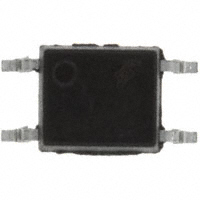
4-Pin Full Pitch Mini-Flat
Package Zero-Cross Triac
Driver Output Optocouplers
MFP4 3.85X4.4, 2.54P
CASE 100AP
FODM3063, FODM3083
MARKING DIAGRAM
Description
The FODM3063 and FODM3083 series consist of an infrared
emitting diode optically coupled to a monolithic silicon detector
performing the function of a zero voltage crossing bilateral triac
driver, and is housed in a compact 4−pin mini−flat package. The lead
pitch is 2.54 mm. They are designed for use with a triac in the interface
of logic systems to equipment powered from 115/240 VAC lines, such
as solid state relays, industrial controls, motors, solenoids and
consumer appliances.
Features
3063
VXYYR
3063 = Device Number
V
= DIN EN/IEC60747−5−5 Option (Only Appears
on Component Ordered with this Option)
X
= One−Digit Year Code, e.g., “6”
YY = Digit Work Week, Ranging from “01” to “53”
R
= Assembly Package Code
• Critical Rate of Rise of Off−Stage Voltage
•
•
•
•
•
♦
dv/dt of 600 V/ms Guaranteed
Zero Voltage Crossing
Peak Blocking Voltage
♦ 600 V (FODM3063)
♦ 800 V (FODM3083)
Compact 4−Pin Surface Mount Package
♦ 2.4 mm Maximum Standoff Height
Safety Regulatory Approvals:
♦ UL1577, 3,750 VACRMS for 1 Minute
♦ DIN−EN/IEC60747−5−5, 565 V Peak Working Insulation Voltage
These are Pb−Free Devices
Applications
•
•
•
•
•
•
•
•
July, 2022 − Rev. 2
ANODE 1
CATHODE 2
4 MAIN TERM.
ZERO
CROSSING
CIRCUIT
3 MAIN TERM.
ORDERING INFORMATION
Solenoid/Valve Controls
Lighting Controls
Static Power Switches
AC Motor Drives
Temperature Controls
E.M. Contactors
AC Motor Starters
Solid State Relays
© Semiconductor Components Industries, LLC, 2006
FUNCTIONAL SCHEMATIC
See detailed ordering and shipping information on page 9 of
this data sheet.
1
Publication Order Number:
FODM3083/D
�FODM3063, FODM3083
SAFETY AND INSULATION RATINGS (As per DIN EN/IEC 60747−5−5, this optocoupler is suitable for “safe electrical insulation”
only within the safety limit data. Compliance with the safety ratings shall be ensured by means of protective circuits.)
Characteristics
Parameter
Installation Classifications per DIN VDE 0110/1.89 Table 1, For Rated Mains Voltage
< 150 VRMS
I–IV
< 300 VRMS
I–III
Climatic Classification
40/100/21
Pollution Degree (DIN VDE 0110/1.89)
2
Comparative Tracking Index
Symbol
175
Value
Unit
Input−to−Output Test Voltage, Method A, VIORM x 1.6 = VPR,
Type and Sample Test with tm = 10 s, Partial Discharge < 5 pC
904
Vpeak
Input−to−Output Test Voltage, Method B, VIORM x 1.875 = VPR,
100% Production Test with tm = 1 s, Partial Discharge < 5 pC
1060
Vpeak
VIORM
Maximum Working Insulation Voltage
565
Vpeak
VIOTM
Highest Allowable Over−Voltage
6000
Vpeak
External Creepage
≥5
mm
External Clearance
≥5
mm
VPR
Parameter
DTI
Distance Through Insulation (Insulation Thickness)
≥0.4
mm
TS
Case Temperature (Note 1)
150
°C
IS,INPUT
Input Current (Note 1)
200
mA
PS,OUTPUT
Output Power (Note 1)
300
mW
Insulation Resistance at TS, VIO = 500 V (Note 1)
>109
W
RIO
1. Safety limit values – maximum values allowed in the event of a failure.
ABSOLUTE MAXIMUM RATINGS (TA = 25°C unless otherwise noted)
Symbol
Value
Unit
TSTG
Storage Temperature
−55 to +150
°C
TOPR
Operating Temperature
−40 to +100
°C
Junction Temperature
−40 to +125
°C
Lead Solder Temperature
260 for 10 s
°C
TJ
TSOL
Parameter
EMITTER
IF (avg)
Continuous Forward Current
60
mA
IF (pk)
Peak Forward Current (1 ms Pulse, 300 pps.)
1
A
Reverse Input Voltage
6
V
100
mW
1
A(PEAK)
VR
PD(EMITTER)
Power Dissipation (No Derating Required over Operating Temp. Range)
DETECTOR
ITSM
Peak Non−Repetitive Surge Current (Single Cycle 60 Hz Sine Wave)
IT(RMS)
On−State RMS Current
VDRM
Off−State Output Terminal Voltage
PD(DETECTOR)
70
mA(RMS)
FODM3063
600
V
FODM3083
800
V
300
mW
Power Dissipation (No Derating Required over Operating Temp. Range)
Stresses exceeding those listed in the Maximum Ratings table may damage the device. If any of these limits are exceeded, device functionality
should not be assumed, damage may occur and reliability may be affected.
www.onsemi.com
2
�FODM3063, FODM3083
ELECTRICAL CHARACTERISTICS (TA = 25°C unless otherwise noted)
Symbol
Parameter
Test Conditions
Min
Typ
Max
Unit
INDIVIDUAL COMPONENT CHARACTERISTICS
EMITTER
VF
Input Forward Voltage
IF = 30 mA
−
−
1.50
V
IR
Reverse Leakage Current
VR = 6 V
−
−
100
mA
DETECTOR
IDRM
Peak Blocking Current Either Direction
Rated VDRM, IF = 0 (Note 2)
dv/dt
Critical Rate of Rise of Off−State Voltage
IF = 0 (Note 3)
−
−
500
nA
600
−
−
V/ms
−
−
5
mA
−
300
−
mA
IF = Rated IFT,
ITM = 100 mA peak
−
−
3
V
Inhibit Voltage, MT1−MT2 Voltage above
which Device will not Trigger
IFT = Rated IFT
−
−
20
V
Leakage in Inhibit State
IFT = Rated IFT, Rated VDRM, Off−State
−
−
2
mA
3,750
−
−
VACRMS
TRANSFER CHARACTERISTICS
IFT
LED Trigger Current
IH
Holding Current, Either Direction
VTM
Peak On−State Voltage, Either Direction
Main Terminal Voltage = 3 V (Note 4)
ZERO CROSSING CHARACTERISTICS
VIH
IDRM2
ISOLATION CHARACTERISTICS
VISO
Steady State Isolation Voltage (Note 5)
1 Minute, R.H. = 40% to 60%
Product parametric performance is indicated in the Electrical Characteristics for the listed test conditions, unless otherwise noted. Product
performance may not be indicated by the Electrical Characteristics if operated under different conditions.
2. Test voltage must be applied within dv/dt rating.
3. This is static dv/dt. Commutating dv/dt is function of the load−driving thyristor(s) only.
4. All devices are guaranteed to trigger at an IF value less than or equal to max IFT. Therefore, recommended operating IF lies between max
IFT (5 mA) and absolute max IF (60 mA).
5. Steady state isolation voltage, VISO, is an internal device dielectric breakdown rating. For this test, pins 1 & 2 are common, and pins 3 & 4
are common.
www.onsemi.com
3
�FODM3063, FODM3083
TYPICAL PERFORMANCE CHARACTERISTICS
1000
1.8
VDRM = 600 V
IDRM, LEAKAGE CURRENT (nA)
VF, FORWARD VOLTAGE (V)
1.7
1.6
1.5
TA= −40°C
1.4
1.3
1.2
TA= 25°C
1.1
TA= 100°C
1.0
10
10
1
0.1
−40
0.9
1
100
100
IF, FORWARD CURRENT (mA)
20
40
60
80
100
Figure 2. Leakage Current vs. Ambient Temperature
1.6
10
NORMALIZED TO TA = 25°C
IFT, TRIGGER CURRENT (NORMALIZED)
IH, HOLDING CURRENT (NORMALIZED)
0
TA, AMBIENT TEMPERATURE (°C)
Figure 1. LED Forward Voltage vs. Forward Current
1.0
0.1
−40
−20
−20
0
20
40
60
80
1.4
1.2
1.0
0.8
0.6
0.8
−40
100
VTM = 3 V
NORMALIZED TO TA = 25°C
−20
0
20
40
60
80
100
TA, AMBIENT TEMPERATURE (°C)
TA, AMBIENT TEMPERATURE (°C)
Figure 3. Holding Current vs. Ambient Temperature
Figure 4. Trigger Current vs. Ambient Temperature
www.onsemi.com
4
�FODM3063, FODM3083
1.4
12
10
VDRM, OFF−STATE OUTPUT TERMINAL
VOLTAGE (NORMALIZED)
TA= 25°C
NORMALIZED TO PWIN >> 100 ms
8
6
4
2
1
10
NORMALIZED TO TA = 25°C
1.3
1.2
1.1
1.0
0.9
0.8
0.7
0.6
−40
0
100
−20
PWIN, LED TRIGGER PULSE WIDTH (°C)
0
TA= 25°C
600
400
200
0
−200
−400
−600
−3
40
60
80
100
Figure 6. Off−State Output Terminal Voltage vs.
Ambient Temperature
800
−800
−4
20
TA, AMBIENT TEMPERATURE (°C)
Figure 5. LED Current Required to Trigger vs.
LED Pulse Width
ITM, ON−STATE CURRENT (mA)
IFT, LED TRIGGER CURRENT (NORMALIZED)
TYPICAL PERFORMANCE CHARACTERISTICS (continued)
−2
−1
0
1
2
VTM, ON−STATE VOLTAGE (V)
Figure 7. On−State Characteristics
www.onsemi.com
5
3
4
�FODM3063, FODM3083
TYPICAL APPLICATION INFORMATION
240 VAC
R1
1
VCC
D1
4
SCR
FODM3063
FODM3083
Rin
2
Suggested method of firing two, back−to−back SCR’s, with a
onsemi triac driver. Diodes can be 1N4001; resistors, R1 and
R2, are optional 330 ohms.
3
SCR
360 W
R2
D2
LOAD
NOTE:
This optoisolator should not be used to drive a load directly. It is intended to be a trigger device only.
Figure 8. Inverse−Parallel SCR Driver Circuit (240 VAC)
www.onsemi.com
6
�FODM3063, FODM3083
DETERMINING THE POWER RATING OF THE SERIES RESISTORS USED IN A ZERO−CROSS
OPTO−TRIAC DRIVER APPLICATION
The power dissipated from resistors placed in series with
the opto−TRIAC and the gate of the power TRIAC is much
smaller than one would expect. These current handling
components only conduct current when the mains voltage is
less than the maximum inhibit voltage. If the opto−TRIAC
is triggered when the mains voltage is greater than the inhibit
voltage, only the TRIAC leakage current will flow. The
power dissipation in a 360 W resistor shown in Figure 9 is the
product of the resistance (360 W) times the square of the
current sum of main TRIAC’s gate current plus the current
flowing gate to the MT2 resistor connection (330 W). This
power calculation is further modified by the duty factor of
the duration for this current flow. The duty factor is the ratio
of the turn−on time of the main TRIAC to the sine of the
single cycle time. Assuming a main TRIAC turn−on time of
50 ms and a 60 Hz mains voltage, the duty cycle is
approximately 0.6 %. The opto−TRIAC only conducts
current while triggering the main TRIAC. Once the main
TRIAC fires, its on−state voltage is typically lower than the
on−state sustaining voltage of the opto−TRIAC. Thus, once
the main TRIAC fires, the opto−TRIAC is often shunted off.
This situation results in very low power dissipation for both
the 360 W and 330 W resistors, when driving a traditional
four quadrant power TRIAC.
If a three quadrant “snubberless” TRIAC is driven by the
opto−TRIAC, the calculations are different. When the main
power TRIAC is driving a high power factor (resistive) load,
it shuts off during the fourth quadrant.
The following will present the calculations for
determining the power dissipation of the current limiting
resistors found in an opto−TRIAC driver interface.
Figure 9 shows a typical circuit to drive a sensitive gate
four quadrant power TRIAC. This figure provides typical
resistor values for a zero line cross detecting opto−TRIAC
when operated from a mains voltage of 20 V to 240 V. The
wattage rating for each resistor is not given because their
dissipation is dependent upon characteristics of the power
TRIAC being driven.
Recall that the opto−TRIAC is used to trigger a four
quadrant power TRIAC. Please note that these opto−TRIACs
are not recommended for driving “snubberless” three
quadrant power TRIACs.
Under normal operation, the opto−TRIAC will fire when
the mains voltage is lower than the minimum inhibit trigger
voltage, and the LED is driven at a current greater than the
maximum LED trigger current. As an example for the
FODM3063, the LED trigger current should be greater than
5 mA, and the mains voltage is less than 10 V peak. The
inhibit voltage has a typical range of 10 V minimum and
20 V maximum. This means that if a sufficient LED current
is flowing when the mains voltage is less than 10 V, the
device will fire. If a trigger appears between 10 V and 20 V,
the device may fire. If the trigger occurs after the mains
voltage has reached 20 Vpeak, the device will not fire.
VCC
Rin
1
4
360 W
FODM3063
FODM3083
2
HOT
39 W*
3
240 VAC
0.01 mH
350 W
LOAD
Typical circuit for use when hot line switching of 240 VAC is required.
In this circuit the “hot” side of the line is switched and the load connected
to the cold or neutral side. The load may be connected to either the
neutral or hot line.
Rin is calculated so that IF is equal to the rated IFT of the part, 5 mA.
The 39 W resistor and 0.01 mF capacitor are for snubbing of the triac
and may or may not be necessary depending upon the particular triac
and load used.
NEUTRAL
*For highly inductive loads (power factor < 0.5), change this value to 360 ohms.
Figure 9. Hot−Line Switching Application Circuit
A 1/4 watt resistor is more than adequate for both the
360 W and 330 W resistors.
The real power in the snubber resistor is based upon the
integral of the power transient present when the load
commutes. A fast commuting transient may allow a peak
current of 4 A to 8 A in the snubbing filter. For best results,
the capacitor should be a non−polarized AC unit with a low
ESR. The 39 W series resistor sets a time constant and limits
the peak current. For a resistive load with a power factor near
unity, the commutating transients will be small. This results
in a very small peak current given the 0.01 mF capacitor’s
reactance. Normally, for factional horse−power reactive
loads, the resistor found in the snubber circuit will have a
power rating from 1/2 W to 2 W. The resistor should be a low
inductance type to adequately filter the high frequency
transients.
If sufficient holding current is still flowing through the
opto−TRIAC, the opto−TRIAC will turn−on and attempt to
carry the power TRIACs load. This situation typically causes
the opto−TRIAC to operate beyond its maximum current
rating, and product and resistor failures typically result. For
this reason, using an opto−TRIAC to drive a three quadrant
“snubberless” power TRIAC is not recommended.
Power in the 360 Ω resistor, when driving a sensitive gate
4 quadrant power TRIAC:
IGT = 20 mA
VGT = 1.5 V
DF = 0.6 %
P = (IGT +VGT / 330 W)2 x 360 W x DF
P = (20 mA + 1.5 / 330 Ω)2 *x 360 W x 0.6 % = 1.3 mW
www.onsemi.com
7
�FODM3063, FODM3083
REFLOW PROFILE
260
240
220
TP
Max. Ramp−up Rate = 3°C/S
Max. Ramp−down Rate = 6°C/S
tP
TL
200
Tsmax
Temperature (°C)
180
160
tL
Preheat Area
Tsmin
140
ts
120
100
80
60
40
20
0
120
240
360
Time 25°C to Peak
Time (seconds)
Profile Freature
Pb−Free Assembly Profile
Temperature Min. (Tsmin)
150°C
Temperature Max. (Tsmax)
200°C
Time (tS) from (Tsmin to Tsmax)
60 – 120 seconds
Ramp−up Rate (tL to tP)
3°C/second max.
Liquidous Temperature (TL)
217°C
Time (tL) Maintained Above (TL)
60–150 seconds
Peak Body Package Temperature
260°C +0°C / –5°C
Time (tP) within 5°C of 260°C
30 seconds
Ramp−down Rate (TP to TL)
6°C/second max.
Time 25°C to Peak Temperature
8 minutes max.
Figure 10. Reflow Profile
www.onsemi.com
8
�FODM3063, FODM3083
ORDERING INFORMATION
Package
Shipping†
FODM3063
Full Pitch Mini−Flat 4−Pin
100 Units / Tube
FODM3063R2
Full Pitch Mini−Flat 4−Pin
2500 Units / Tape & Reel
FODM3063V
Full Pitch Mini−Flat 4−Pin, DIN EN/IEC60747−5−5 Option
100 Units / Tube
FODM3063R2V
Full Pitch Mini−Flat 4−Pin, DIN EN/IEC60747−5−5 Option
2500 Units / Tape & Reel
Part Number
†For information on tape and reel specifications, including part orientation and tape sizes, please refer to our Tape and Reel Packaging
Specifications Brochure, BRD8011/D.
NOTE: The product orderable part number system listed in this table also applies to the FODM3083 products.
FOOTPRINT DRAWING FOR PCB LAYOUT
0.80
1.00
6.50
2.54
NOTE:
All dimensions are in mm.
Figure 11. Footprint Drawing for PCB Layout
www.onsemi.com
9
�MECHANICAL CASE OUTLINE
PACKAGE DIMENSIONS
MFP4 3.85X4.4, 2.54P
CASE 100AP
ISSUE O
DOCUMENT NUMBER:
DESCRIPTION:
98AON13488G
MFP4 3.85X4.4, 2.54P
DATE 31 AUG 2016
Electronic versions are uncontrolled except when accessed directly from the Document Repository.
Printed versions are uncontrolled except when stamped “CONTROLLED COPY” in red.
PAGE 1 OF 1
ON Semiconductor and
are trademarks of Semiconductor Components Industries, LLC dba ON Semiconductor or its subsidiaries in the United States and/or other countries.
ON Semiconductor reserves the right to make changes without further notice to any products herein. ON Semiconductor makes no warranty, representation or guarantee regarding
the suitability of its products for any particular purpose, nor does ON Semiconductor assume any liability arising out of the application or use of any product or circuit, and specifically
disclaims any and all liability, including without limitation special, consequential or incidental damages. ON Semiconductor does not convey any license under its patent rights nor the
rights of others.
© Semiconductor Components Industries, LLC, 2019
www.onsemi.com
�onsemi,
, and other names, marks, and brands are registered and/or common law trademarks of Semiconductor Components Industries, LLC dba “onsemi” or its affiliates
and/or subsidiaries in the United States and/or other countries. onsemi owns the rights to a number of patents, trademarks, copyrights, trade secrets, and other intellectual property.
A listing of onsemi’s product/patent coverage may be accessed at www.onsemi.com/site/pdf/Patent−Marking.pdf. onsemi reserves the right to make changes at any time to any
products or information herein, without notice. The information herein is provided “as−is” and onsemi makes no warranty, representation or guarantee regarding the accuracy of the
information, product features, availability, functionality, or suitability of its products for any particular purpose, nor does onsemi assume any liability arising out of the application or use
of any product or circuit, and specifically disclaims any and all liability, including without limitation special, consequential or incidental damages. Buyer is responsible for its products
and applications using onsemi products, including compliance with all laws, regulations and safety requirements or standards, regardless of any support or applications information
provided by onsemi. “Typical” parameters which may be provided in onsemi data sheets and/or specifications can and do vary in different applications and actual performance may
vary over time. All operating parameters, including “Typicals” must be validated for each customer application by customer’s technical experts. onsemi does not convey any license
under any of its intellectual property rights nor the rights of others. onsemi products are not designed, intended, or authorized for use as a critical component in life support systems
or any FDA Class 3 medical devices or medical devices with a same or similar classification in a foreign jurisdiction or any devices intended for implantation in the human body. Should
Buyer purchase or use onsemi products for any such unintended or unauthorized application, Buyer shall indemnify and hold onsemi and its officers, employees, subsidiaries, affiliates,
and distributors harmless against all claims, costs, damages, and expenses, and reasonable attorney fees arising out of, directly or indirectly, any claim of personal injury or death
associated with such unintended or unauthorized use, even if such claim alleges that onsemi was negligent regarding the design or manufacture of the part. onsemi is an Equal
Opportunity/Affirmative Action Employer. This literature is subject to all applicable copyright laws and is not for resale in any manner.
PUBLICATION ORDERING INFORMATION
LITERATURE FULFILLMENT:
Email Requests to: orderlit@onsemi.com
onsemi Website: www.onsemi.com
◊
TECHNICAL SUPPORT
North American Technical Support:
Voice Mail: 1 800−282−9855 Toll Free USA/Canada
Phone: 011 421 33 790 2910
Europe, Middle East and Africa Technical Support:
Phone: 00421 33 790 2910
For additional information, please contact your local Sales Representative
�