Is Now Part of
To learn more about ON Semiconductor, please visit our website at
www.onsemi.com
Please note: As part of the Fairchild Semiconductor integration, some of the Fairchild orderable part numbers
will need to change in order to meet ON Semiconductor’s system requirements. Since the ON Semiconductor
product management systems do not have the ability to manage part nomenclature that utilizes an underscore
(_), the underscore (_) in the Fairchild part numbers will be changed to a dash (-). This document may contain
device numbers with an underscore (_). Please check the ON Semiconductor website to verify the updated
device numbers. The most current and up-to-date ordering information can be found at www.onsemi.com. Please
email any questions regarding the system integration to Fairchild_questions@onsemi.com.
ON Semiconductor and the ON Semiconductor logo are trademarks of Semiconductor Components Industries, LLC dba ON Semiconductor or its subsidiaries in the United States and/or other countries. ON Semiconductor owns the rights to a number
of patents, trademarks, copyrights, trade secrets, and other intellectual property. A listing of ON Semiconductor’s product/patent coverage may be accessed at www.onsemi.com/site/pdf/Patent-Marking.pdf. ON Semiconductor reserves the right
to make changes without further notice to any products herein. ON Semiconductor makes no warranty, representation or guarantee regarding the suitability of its products for any particular purpose, nor does ON Semiconductor assume any liability
arising out of the application or use of any product or circuit, and specifically disclaims any and all liability, including without limitation special, consequential or incidental damages. Buyer is responsible for its products and applications using ON
Semiconductor products, including compliance with all laws, regulations and safety requirements or standards, regardless of any support or applications information provided by ON Semiconductor. “Typical” parameters which may be provided in ON
Semiconductor data sheets and/or specifications can and do vary in different applications and actual performance may vary over time. All operating parameters, including “Typicals” must be validated for each customer application by customer’s
technical experts. ON Semiconductor does not convey any license under its patent rights nor the rights of others. ON Semiconductor products are not designed, intended, or authorized for use as a critical component in life support systems or any FDA
Class 3 medical devices or medical devices with a same or similar classification in a foreign jurisdiction or any devices intended for implantation in the human body. Should Buyer purchase or use ON Semiconductor products for any such unintended
or unauthorized application, Buyer shall indemnify and hold ON Semiconductor and its officers, employees, subsidiaries, affiliates, and distributors harmless against all claims, costs, damages, and expenses, and reasonable attorney fees arising out
of, directly or indirectly, any claim of personal injury or death associated with such unintended or unauthorized use, even if such claim alleges that ON Semiconductor was negligent regarding the design or manufacture of the part. ON Semiconductor
is an Equal Opportunity/Affirmative Action Employer. This literature is subject to all applicable copyright laws and is not for resale in any manner.
�FSA880 / FSA881 – USB Port 2:1 Switch with Accessory
and Charger Detection
Features
Description
Switch Type
2:1 USB
Automatic switching with Available
Switch Mechanism
Interrupt
USB Data Cable
Chargers (CDP, DCP, Travel Adapter,
Accessory Detection
Car Kit-CEA-936-A)
Factory-Mode Cables
USB
FS and HS 2.0 Compliant
Battery Charging 1.1 Compliant
USB Charging
Charger Detect, DCD, OVT (28 V)
UART
RxD and TxD
VBAT
3.0 to 4.4 V
2
Programmability
IC
ESD
15kV IEC 61000-4-2 Air Gap
Operating
-40°C to 85°C
Temperature
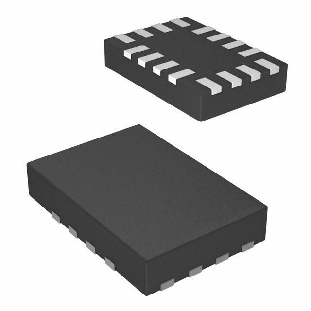
16-Lead UMLP
Package
1.8x2.6x0.55 mm, 0.4 mm Pitch
FSA880 – Active LOW
JIG Option
FSA881 – Active HIGH
FSA880UMX
Ordering Information
FSA881UMX
The FSA88x is a high-performance switch featuring
automatic switching and accessory detection for a USB port.
The FSA88x allows sharing of a common USB port to pass
USB data, as well as factory programmability. In addition,
the FSA88x integrates accessory detection of devices such
as USB chargers and factory data cables. The FSA88x can
be programmed for manual switching or automatic switching
of data paths. VBUS_IN has 28 V over-voltage tolerance.
The difference between the FSA880 and the FSA881 is that
FSA880 JIG output is an open-drain, active-LOW output,
while FSA881 JIG is an active-HIGH, CMOS output.
Applications
Cellular Phones, Smart Phones
MP3 and PMP
Related Resources
FSA880 / FSA881 Demonstration Board
Typical Application
USB Data
USB CHARGING
FACTORY TEST
OVT
PROTECTION
FSA88x
FSA9280A
Figure 1.
© 2010 Fairchild Semiconductor Corporation
FSA880 / FSA881 • Rev. 1.0.7
Mobile Phone Example
www.fairchildsemi.com
FSA880 / FSA881 — USB Port 2:1 Switch with Accessory and Charger Detection
August 2014
�Part Number
Operating Temperature Range
Top Mark
Package
FSA880UMX
-40 to +85°C
KU
16-Lead, Ultrathin Molded Leadless Package (UMLP),
1.8 mm x 2.6 mm x 0.55 mm, 0.4 mm Pitch
FSA881UMX
-40 to +85°C
KX
16-Lead, Ultrathin Molded Leadless Package (UMLP),
1.8 mm x 2.6 mm x 0.55 mm, 0.4 mm Pitch
Block Diagram
FSA880
V BAT
Phone
Power
V BUS_IN
Detection
28V OVT
V DDIO
HS USB
or UART
HS USB
Interrupt
I2C
Baseband
Processor
DM_HOST
DP_HOST
2:1
MUX
V DDIO
100kΩ
JIG
BOOT
ID_CON
Charger
Detect BC1.1
Switch
Control
and
I2C
Slave
GND
Float
Detect
ADC ID
Detect
Figure 2.
© 2010 Fairchild Semiconductor Corporation
FSA880 / FSA881 • Rev. 1.0.7
DM_CON
DP_CON
DM_HOST1
DP_HOST1
INTB
I2C_SCL
I2C_SDA
USB Port
Block Diagram
www.fairchildsemi.com
2
FSA880 / FSA881 — USB Port 2:1 Switch with Accessory and Charger Detection
Ordering Information
�FSA880 / FSA881 — USB Port 2:1 Switch with Accessory and Charger Detection
Pin Configuration
ID_CON DP_CON DM_CON VBUS_IN
16
DM_HOST
15
14
1
13
12
GND
DP_HOST
2
11
I2C_SDA
DM_HOST1
3
10
I2C_SCL
DP_HOST1
4
9
INTB
5
6
7
8
VBAT
BOOT
JIG
VDDIO
Figure 3.
© 2010 Fairchild Semiconductor Corporation
FSA880 / FSA881 • Rev. 1.0.7
Pin Assignment (Through View)
www.fairchildsemi.com
3
�Name
Pin #
Type
Default
State
Description
USB/UART Interface
DP_HOST
2
Signal Path
Open
D+ signal switch path, dedicated USB port to be connected to the
resident USB / UART on the phone. Default port for all USB
accessories and USB factory modes.
DM_HOST
1
Signal Path
Open
D- signal switch path, dedicated USB port to be connected to the
resident USB / UART on the phone. Default port for all USB
accessories and USB factory modes.
VBUS_IN
13
Input
N/A
Input voltage supply pin to be connected to the VBUS pin of the USB
connector
USB/UART Interface 1
DM_HOST1
3
Signal Path
Open
D- signal switch path, dedicated USB port to be connected to the
secondary resident USB / UART on the phone. Default port for UART
factory modes.
DP_HOST1
4
Signal Path
Open
D+ signal switch path, dedicated USB port to be connected to the
secondary resident USB / UART on the phone. Default port for UART
factory modes.
Connector Interface
GND
12
Ground
N/A
Ground
ID_CON
16
Signal Path
Open
Connected to the USB connector ID pin and used for detecting
accessories
DP_CON
15
Signal Path
Open
Connected to the USB connector D+ pin; depending on the signaling
mode, this pin can be switched to DP_HOST or RxD_HOST pins.
DM_CON
14
Signal Path
Open
Connected to the USB connector D- pin; depending on the signaling
mode, this pin can switched to DM_HOST or TxD_HOST pins.
VDDIO
8
Power
N/A
Input baseband interface I/O supply pin
VBAT
5
Power
N/A
Input voltage supply pin to be connected to the mobile phone battery
output or to an internal regulator on the phone
JIG
7
FSA880:
Open-Drain
Output
FSA881:
CMOS
Output
FSA880:Hi-Z
FSA881:
LOW
Output control signal and used by the processor for factory test modes
FSA880: Active LOW open-drain output
FSA881: Active HIGH CMOS output
BOOT
6
CMOS
Output
LOW
Output control signal and used by the processor for factory test modes
I2C_SCL
10
Input
Hi-Z
I C serial clock signal to be connected to the phone-based I C master
I2C_SDA
11
Open-Drain
I/O
Hi-Z
I C serial data signal to be connected to the phone-based I C master
INTB
9
CMOS
Output
LOW
Interrupt active LOW output used to prompt the phone baseband
2
processor to read the I C register bits, indicate a change in ID_CON
pin status or accessories’ attach status
Power Interface
Factory Interface
2
I C Interface
2
2
2
2
Note:
1. LOW = VOL or VIL; HIGH = VOH or VIH.
© 2010 Fairchild Semiconductor Corporation
FSA880 / FSA881 • Rev. 1.0.7
www.fairchildsemi.com
4
FSA880 / FSA881 — USB Port 2:1 Switch with Accessory and Charger Detection
Pin Descriptions
�Functionality
The FSA88x is USB port accessory detector and switch with
integrated 28 V over-voltage tolerance. Fully controlled using
2
I C, FSA88x enables high-speed USB 2.0 Standard
Downstream Port (SDP), USB Charging Downstream Port
(CDP) battery charger, USB Dedicated Charging Port (DCP)
charger data cables to use a common connector micro or
mini USB 2.0 port. Factory-mode cables can be detected
and switched to use either the UART or USB data path. The
FSA88x can be programmed for manual switching or
automatic switching of data paths.
Flow Diagram
Power-up &
Reset
The architecture uses ID pin detection for convenient factory
testing. Figure 9 - Figure 13 show the FSA88x passing the
USB eye compliance test with ample margin.
1.1.
Functional Overview
The FSA88x is designed for minimal software requirements
for proper operation. The flow diagram in Figure 4 walks
through the fundamental steps of operation and contains
references to more detailed information.
State
Datasheet
Section
Power-Up & Reset
Section 2
Applies power to the device and resets state
of the device
Section 3
Communication with device through I C
Configuration
Section 4
Configures the device using I C and the
internal registers (which can be bypassed
during power-up)
Detection
Section 5
Manages accessory detection, including
attachment and detachment
Processor
Communication
Section 6
How the detection of the accessory is
indicated to the processor
Switch
Configuration
Section 7
Configuration of switches based on detection
Active Signal
Section 8
Signal performance of selected configuration
2
IC
Description
2
2
I2C
Configuration
Accessory
Plug-in
Detection
Processor
Communication
Switch
Configuration
Active Signals
Accessory
Detached
Figure 4.
Basic Operation Flow
© 2010 Fairchild Semiconductor Corporation
FSA880 / FSA881 • Rev. 1.0.7
www.fairchildsemi.com
5
FSA880 / FSA881 — USB Port 2:1 Switch with Accessory and Charger Detection
1.
�Power-Up & Reset
The FSA88x does not need special power sequencing for
correct operation. The main power is provided by VBAT only.
2
VDDIO is only used for I C interface and interrupt processing.
Table 1 summarizes the enabled features of each power
state. The valid voltages levels for each power supply can be
found in Section 9.
Table 1. Power States Summary
Enabled Functionality
Valid
VBUS_IN
Valid
(1)
VDDIO
Valid VBAT
Power State
X
N
X
N
N
Power Down
NO
Not Typical
Illegal State
X
Y
N
Powered from VBAT
NO
YES
X
Y
Y
Powered from VBAT
YES
YES
(2)
Y
Processor
Communication
2
(I C & Interrupts)
Detection
Notes:
1. VDDIO is expected to be the same supply used by the baseband I/Os.
2. Typically VDDIO is only present when VBAT is valid.
3. X = Don’t care.
2.1.
Reset
2.1.1. Hardware Reset
Power-on reset is caused by the initial rising edge of VBAT
When the device is reset, all the registers are initialized to
the default values shown in Section 9.9 and all switch paths
are open. After reset or power up, FSA88x enters Standby
Mode and is ready to detect accessories sensed on its
VBUS_IN and / or ID_CON pins.
© 2010 Fairchild Semiconductor Corporation
FSA880 / FSA881 • Rev. 1.0.7
2.1.2. Software Reset
The device can be reset through software by writing to the
Reset bit in the Register (1BH).
www.fairchildsemi.com
6
FSA880 / FSA881 — USB Port 2:1 Switch with Accessory and Charger Detection
2.
�I2C
2
The FSA88x integrates a full fast-mode I C slave controller
2
compliant with the I C specification version 2.1. The FSA88x
2
I C interface runs up to 400 kHz.
The slave address is shown in Table 2. Status information
2
and configuration occurs via the I C interface. Please see
Table 7 for more information.
2
Table 2. I C Slave Address
Name
Size (Bits)
Bit 7
Bit 6
Bit 5
Bit 4
Bit 3
Bit 2
Bit 1
Bit 0
Slave Address
8
0
1
0
0
1
0
1
Read / Write
8bits
S
Slave
Address
Note:
WR
A
8bits
8bits
Register
Address K
Write
Data
A
A
8bits
A
Write Data
K+N-1
A
P
8bits
2
I C Write Sequence
8bits
8bits
S Slave Address WR A Register Address K A S Slave Address RD A
Register address to Read specified
Note:
Read Data K
A Read Data K+1 A Read Data K+N-1 NA P
Single or multi byte read executed from current register location (Single Byte read is
initiated by Master with NA immediately following first data byte)
If Register is not specified Master will begin read from current register. In this case only sequence showing in Red
bracket is needed
Figure 6.
From Master to Slave
From Slave to Master
S
A
2
I C Read Sequence
NA NOT Acknowledge (SDA High)
WR Write=0
Start Condition
Acknowledge (SDA Low)
RD
P
Read =1
Stop Condition
Configuration
a.
FSA88x requires minimal configuration for proper detection
and reporting. The following steps provide full configuration.
1.
A
Write
Data
K+2
Single-byte write is initiated by Master with P immediately following first data byte.
Figure 5.
4.
Write
Data
K+1
2.
Write Control register (02h) to configure manual or
automatic switching modes.
© 2010 Fairchild Semiconductor Corporation
FSA880 / FSA881 • Rev. 1.0.7
If using manual switching modes, write Manual SW
1 register (13h) to configure switches.
Write Control register (02h) to clear INT Mask bit.
This enables interrupts to the baseband.
www.fairchildsemi.com
7
FSA880 / FSA881 — USB Port 2:1 Switch with Accessory and Charger Detection
3.
�Detection
The FSA88x monitors both VBUS_IN and ID_CON to detect
accessories. The ID_CON detection is a “resistive detection”
that reads the resistance to GND on the ID_CON pin to
determine the accessory attached. Table 3 shows the
assignment of accessories based on resistor values.
FSA88x can also detect accessories with ID resistances
outside the specified ranges. The FSA88x detects these
unknown accessories in the same manner as the defined
accessories and interrupts the baseband processor and
provides the correct ADC value, as shown in Table 3.
Table 3. ID_CON Accessory Detection
ADC Code
Equivalent RID
Description
4
3
2
1
0
Min.
Target
Max.
1
0
1
0
1
117.4 kΩ
121 kΩ
124.6 kΩ
Unknown Accessory
1
0
1
1
0
145.5 kΩ
150 kΩ
154.5 kΩ
Unknown Accessory
(4)
1
0
1
1
1
176.4 kΩ
206 kΩ
Travel Adapter (TA) or Car Kit Type 1 Charger
1
1
0
0
0
247.3 kΩ
255 kΩ
262.7 kΩ
Factory Mode Boot OFF-USB
1
1
0
0
1
291.9 kΩ
301 kΩ
310.1 kΩ
Factory Mode Boot ON-USB
1
1
0
1
0
354 kΩ
1
1
0
1
1
428.7 kΩ
1
1
1
0
0
507.3 kΩ
1
1
1
0
1
1
1
1
1
0
Not ‘h1F or any code above
200 kΩ
375.9 kΩ
Unknown Accessory
455.3 kΩ
Unknown Accessory
523 kΩ
538.7 kΩ
Factory Mode Boot OFF-UART
600.4 kΩ
619 kΩ
637.6 kΩ
Factory Mode Boot ON-UART
750 kΩ
1000 kΩ
1030 kΩ
Unknown Accessory
3 MΩ
365 kΩ
(4)
442 kΩ
None of the above ranges
Unknown Accessory
Note:
4. These accessories need VBUS to be valid in order to be detected since they are charger accessories.
5.1.
Factory Cable Detection
Factory modes are initiated with the attachment of special
test hardware, called a “JIG box” for factory testing. The
FSA88x automatically configures switch paths to any of the
factory-mode accessories when the appropriate resistor is
sensed on the ID_CON pin. A change of resistor on the
ID_CON pin dynamically switches between factory modes
and auto-configures the appropriate switch paths without
detaching and attaching the cable.
and the JIG and BOOT logic states are listed in Table 4. The
FSA88x allows both HS USB and FS USB in addition to
UART signals to be passed on both ports with matched
performance. This allows greater flexibility when designing
with the FSA88x.
JIG output signals when a factory mode accessory is plugged
in and BOOT output signals the mobile phone to boot up. The
switch paths for factory modes are shown in Table 4.
The different factory mode accessories with the associated
resistor values (1% standard resistors) on the ID_CON pin
Table 4. ID_CON Factory Cable Detection
ID_CON
DP_CON
DM_CON
Factory Mode Boot_On
Jig: UART
Boot_Off
DP_HOST1
DM_HOST1
600kΩ
619kΩ
637kΩ
HIGH
LOW
HIGH
DP_HOST1
DM_HOST1
507kΩ
523kΩ
538kΩ
LOW
LOW
HIGH
Factory Mode Boot_On
Jig: USB
Boot_Off
DP_Host
DM_Host
292kΩ
301kΩ
310kΩ
HIGH
LOW
HIGH
DP_Host
DM_Host
247kΩ
255kΩ
262kΩ
LOW
LOW
HIGH
The FSA88x detection algorithms monitor both the VBUS and
ID pins of the USB interface. Based on the detection results,
multiple registers are updated and the INTB pin is asserted
to indicate to the baseband processor that an accessory was
detected and to read the registers for the complete
© 2010 Fairchild Semiconductor Corporation
FSA880 / FSA881 • Rev. 1.0.7
BOOT
FSA880 FSA881
JIG
JIG
Configuration Type
information. The detection algorithm allows the application to
control the timing of the detection algorithm and the
configuration of the internal switches. The flow diagram in
Figure 7 shows the operation of the detection algorithm.
www.fairchildsemi.com
8
FSA880 / FSA881 — USB Port 2:1 Switch with Accessory and Charger Detection
5.
�FSA880 / FSA881 — USB Port 2:1 Switch with Accessory and Charger Detection
Factory JIG Box
Attached
FSA880 Detects
Attachment
FSA880 Writes
Device Register
and Asserts JIG
NO
VDDIO
HIGH?
YES
INTB Asserted and
Switch Paths AutoConfigured
µP Reads Interrupt
Registers
FSA880 Enters
Standby
YES
NO
ID Float >70ms
YES
NO
Exit Factory Mode
Accessory Flow
NO
ID Change?
YES
Rid=Factory
Mode
Figure 7.
© 2010 Fairchild Semiconductor Corporation
FSA880 / FSA881 • Rev. 1.0.7
Factory Cable Detection Flow Chart (FSA880)
www.fairchildsemi.com
9
�USB Port Detection
The multiple types of USB 2.0 ports the FSA88x can detect are summarized in Table 5.
Table 5. ID_CON and VBUS Detection Table for USB Devices
VBUS_IN
DP_CON
DM_CON
5V
Not Checked
5V
5V
ID_CON resistance to GND
Accessory Detected
(5)
Min.
Typ.
Max.
Not Checked
174.6 kΩ
200 kΩ
206 kΩ
TA (travel adapter) Charger (180 kΩ) and
(6)
Car Kit Charger Type 1 only (200 kΩ)
Shorted to
DM_CON
Shorted to
DP_CON
3 MΩ
Open
Open
USB Dedicated Charging Port, Travel
(6)
Adapter or Dedicated Charger (DCP)
DP_HOST
DM_HOST
3 MΩ
Open
Open
USB Charging Downstream Port (CDP)
(6)
(6)
5V
DP_HOST
DM_HOST
3 MΩ
Open
Open
USB Standard Downstream Port (SDP)
Notes:
5. The accessory type is reported in the Device Type 1 (0Ah) register for each valid accessory detected.
6. The FSA88x follows the Battery Charging 1.1 specification, which uses DP_CON and DM_CON to determine the USB
accessory attached. Refer to Battery Charging 1.1 specification for further details.
For SDP and CDP USB accessories, the following pin mapping is automatically configured:
DP_HOST = DP_CON
DM_HOST = DM_CON
For DCP charger, the DP_HOST and DM_HOST switches are open. For all USB accessories VBUS_IN is Over-Voltage
Tolerance (OVT) up to 28 V.
6.
Processor Communication
Typical communication steps between the processor and the
FSA88x during accessory detection are:
a. Device Type 1 (0Ah): Indicates which USB, Car Kit
CDP, or DCP accessory was detected.
1.
INTB is asserted LOW, indicating change in accessory
detection.
b. Device Type 2 (0Bh): Indicates which factory mode or
unknown accessory was detected.
2.
Processor reads Interrupt 1 (03h) register to determine if
an attach or detach event was detected.
3.
Processor reads Status registers to determine the exact
accessory detected.
© 2010 Fairchild Semiconductor Corporation
FSA880 / FSA881 • Rev. 1.0.7
www.fairchildsemi.com
10
FSA880 / FSA881 — USB Port 2:1 Switch with Accessory and Charger Detection
5.2.
�Switch Configuration
FSA88x devices have two modes of operation when
configuring the internal switches. The FSA88x can autoconfigure the switches or the switches can be configured
7.1.
manually by the processor. Typical applications use AutoConfiguration Mode and do not require interaction with the
baseband to configure the switches correctly.
Configurations
FSA880
VBAT
Phone
Power
HS USB
or UART
USB Accessories and
Factory Cables:
DP_CON=DP_HOST
DM_CON=DM_HOST
HS USB
Interrupt
I2C
Baseband
Processor
VBUS_IN
Detection
28V OVT
VDDIO
DM_HOST
DP_HOST
2:1
MUX
ID_CON
Charger
Detect BC1.1
INTB
I2C_SCL
I2C_SDA
Switch
Control
and
I2C
Slave
VDDIO
100k
W
JIG
BOOT
ADC ID
Detect
VBAT
UART Factory
Cables:
DP_CON=DP_HOST1
DM_CON=DM_HOST1
HS USB
Interrupt
I2C
Baseband
Processor
DM_HOST
DP_HOST
2:1
MUX
DM_CON
DP_CON
DM_HOST1
DP_HOST1
ID_CON
Charger
Detect BC1.1
INTB
I2C_SCL
I2C_SDA
Switch
Control
and
I2C
Slave
VDDIO
100k
W
JIG
BOOT
7.2.
USB Port
VBUS_IN
Detection
28V OVT
VDDIO
Figure 8.
GND
Float
Detect
FSA880
HS USB
or UART
DM_CON
DP_CON
DM_HOST1
DP_HOST1
Phone
Power
USB Port
GND
Float
Detect
ADC ID
Detect
Switch Configurations
Manual Switching
Manual switching is enabled by writing the following registers:
Manual Switch 1 (13h): Configures the switches for DM_CON, and DP_CON.
Manual Switch 2 (14h): Configures the BOOT, and JIG pins.
© 2010 Fairchild Semiconductor Corporation
FSA880 / FSA881 • Rev. 1.0.7
www.fairchildsemi.com
11
FSA880 / FSA881 — USB Port 2:1 Switch with Accessory and Charger Detection
7.
�Active Signal Performance
8.1.
HS USB Data
8.1.1.
DP_HOST/DM_HOST
Figure 9.
8.1.2.
Pass Through Eye Compliance Testing
Input Signal
Figure 10.
USB 2.0 Eye Compliance Test Results
at Output
Figure 12.
USB 2.0 Eye Compliance Test Results
at Output
DP_HOST1/DM_HOST1
Figure 11.
Pass-Through Eye Compliance Testing
Input Signal
© 2010 Fairchild Semiconductor Corporation
FSA880 / FSA881 • Rev. 1.0.7
www.fairchildsemi.com
12
FSA880 / FSA881 — USB Port 2:1 Switch with Accessory and Charger Detection
8.
�Full-Speed USB
8.2.1.
DP_HOST/DM_HOST
8.2.2.
Figure 13.
USB FS Eye Compliance Testing
Figure 14.
USB FS Eye Compliance Testing
FSA880 / FSA881 — USB Port 2:1 Switch with Accessory and Charger Detection
8.2.
DP_HOST1/DM_HOST1
© 2010 Fairchild Semiconductor Corporation
FSA880 / FSA881 • Rev. 1.0.7
www.fairchildsemi.com
13
�Product Specifications
9.1.
Absolute Maximum Ratings
Stresses exceeding the absolute maximum ratings may damage the device. The device may not function or be operable
above the recommended operating conditions and stressing the parts to these levels is not recommended. In addition,
extended exposure to stresses above the recommended operating conditions may affect device reliability. The absolute
maximum ratings are stress ratings only.
Symbol
VBAT
VBUS_IN
VSW
Parameter
Min.
Max.
Unit
Supply Voltage from Battery
-0.5
6.0
V
Supply Voltage from USB Connector
-0.5
28.0
V
USB
-1.0
6.0
UART
-1.0
6.0
Switch I/O Voltage
IIK
Input Clamp Diode Current
ISW
Switch I/O Current (Continuous)
ISWPEAK
TSTG
-50
mA
USB at TA=85°C
25
UART at TA=85°C
12
Peak Switch Current (Pulsed at 1ms Duration, 2 V
0.05 VDDIO
V
VDDIO2 V
0.4
VDDIO2 V
0.05 VDDIO
V
VDDIO2 V
0.4
VDDIO4.0 V
USB Switches Closed
VBUS_IN
FLOAT
XXXXXXXXXXXXXXXXXXXXXXXXXXXXXXXXXXXXXXXXXXXXXXXXX
FLOAT
ID Resistance
DCD Checking 20 ms
ID Detection Time110ms
Open
USB Switch State
Closed
130ms
Figure 18.
USB Standard Downstream Port Attach Timing
VBUS > 4. 0V
INTB Asserted and
Registers Written
VBUS Voltage
XXXXXXXXXXXXXXXXXXXXXXXXXXXXXXXXXXXXXXXXXXXXXXXXX
FLOAT
FLOAT
ID Resistance
170ms
Switch State
Closed ( CDP Only)
INTB Pin
DCD- 20ms
Figure 19.
© 2010 Fairchild Semiconductor Corporation
FSA880 / FSA881 • Rev. 1.0.7
CHG DETECTION 150ms
USB Charging Ports (DCP & CDP) Attach Timing
www.fairchildsemi.com
18
�FSA880 / FSA881 — USB Port 2:1 Switch with Accessory and Charger Detection
VBUS >4.0V
VBUS_iN
_
ID ResistanceXXXXXXXX
FLOAT
JIG Pin
ID Detection Time 200 ms
BOOT Pin
Open
Switch State
Closed
Figure 20.
ID Resistance
Jig Box Attach Timing (VBUS_IN Valid)
FLOAT
XXXXXX
JIG Pin
ID Detection Time 200ms
BOOT Pin
Open
Switch State
Closed
Figure 21.
© 2010 Fairchild Semiconductor Corporation
FSA880 / FSA881 • Rev. 1.0.7
JIG Box Attach Timing without VBUS_IN
www.fairchildsemi.com
19
�Programmability Tables
2
Table 7. I C Register Map
Address Register Type
01H
Device ID
Reset
(12,13)
Value
R
(14)
(14)
Bit 6
Bit 7
N/A
02H
Control
R/W
03H
Interrupt
R/C
xxxxxx00
07H
ADC
R
xxx11111
0AH
Device
Type 1
R
x000x0xx
0BH
Device
Type 2
R
0xxx0000
13H
Manual
SW 1
R/W
000000xx
14H
Manual
SW 2
R/W
xxxx00xx
1BH
Reset
R/W
xxxxxxx0
(14)
Bit 5
(14)
Bit 4
(14)
(14)
Bit 3
Revision Number
Bit 1
(14)
Bit 0
Vendor ID
Switch
Open
xxx0x1x1
(14)
Bit 2
Auto
Config
INT
Mask
Detach
Attach
ADC Value
Dedicated USB
Charger Charger
(CDP)
(DCP)
Car Kit
Type 1
& TA
Charger
Unknown
Accessory
Standard
USB
(SDP)
Jig UART
Off
D- Switching
Jig
UART
On
Jig USB Jig USB
Off
On
D+ Switching
BOOT
SW
JIG ON
Reset
Notes:
12. Write “0” to undefined register bits.
13. Values read from undefined register bits are not defined and invalid.
14. Do not use undefined register locations.
Table 8. Device ID
Address: 01h
Type: Read
Bit #
Name
Size (Bits)
Description
7:3
Revision Number
5
Rev 0.0 = 00000
2:0
Vendor ID
3
000: Fairchild Semiconductor
Table 9. Control
Address: 02h
Reset Value: xxx0x1x1
Type: Read/Write
Bit #
Name
Size (Bits)
7:5
DoNotUse
3
N/A
4
Switch Open
1
1: Open all switches
0: Automatic switching by accessory status
3
DoNotUse
1
N/A
2
Auto Config
1
1: Automatic switching (also called auto-configuration)
0: Manual switching
1
DoNotUse
1
N/A
0
INT Mask
1
1: Mask interrupt – do not interrupt baseband processor
0: Unmask interrupt – interrupt baseband processor on change of state in
Interrupt register
© 2010 Fairchild Semiconductor Corporation
FSA880 / FSA881 • Rev. 1.0.7
Description
www.fairchildsemi.com
20
FSA880 / FSA881 — USB Port 2:1 Switch with Accessory and Charger Detection
9.9.
�Address: 03h
Reset Value: xxxxxx00
Type: Read/Clear
Bit #
Name
Size (Bits)
Description
7:2
DoNotUse
6
N/A
1
Detach
1
1: Accessory detached
0: Accessory not detached
0
Attach
1
1: Accessory attached
0: Accessory not attached
Table 11. Device Type 1
Address: 07h
Reset Value: xxx11111
Type: Read
Bit #
Name
Size (Bits)
Description
7:5
Reserved
3
NA
4:0
ADC Value
5
ADC value read from ID
Table 12. Device Type 1
Address: 0Ah
Reset Value: x00x00xx
Type: Read
Bit #
Name
Size (Bits)
7
DoNotUse
1
N/A
Description
6
Dedicated Charger
(DCP)
1
1: USB dedicated charging port (DCP) charger detected
0: USB dedicated charging port (DCP) charger not detected
5
USB Charger (CDP)
1
1: USB charging downstream port (CDP) charger detected
0: USB charging downstream port (CDP) charger not detected
4
Car Kit Type 1 & TA
Charger
1
1: Car Kit Type 1 or Travel Adapter (TA) detected
0: Car Kit Type 1 or Travel Adapter (TA) not detected
3
DoNotUse
1
N/A
2
Standard USB
(SDP)
1
1: USB standard downstream port (SDP) detected
0: USB standard downstream port (SDP) not detected
1:0
DoNotUse
2
N/A
Table 13. Device Type 2
Address: 0Bh
Reset Value: 0xxx0000
Type: Read
Bit #
Name
Size (Bits)
7
Unknown Accessory
1
1: Any accessory detected as unknown or an accessory that cannot be
detected as being valid even though ID_CON is not floating
0: Unknown accessory not detected
6:4
DoNotUse
4
N/A
3
JIG_UART_OFF
1
1: Factory mode BOOT-OFF-UART detected
0: Factory mode BOOT-OFF-UART not detected
© 2010 Fairchild Semiconductor Corporation
FSA880 / FSA881 • Rev. 1.0.7
Description
www.fairchildsemi.com
21
FSA880 / FSA881 — USB Port 2:1 Switch with Accessory and Charger Detection
Table 10. Interrupt
�Name
Size (Bits)
Description
2
JIG_UART_ON
1
1: Factory mode cable UART path with BOOT ON detected
0: Factory mode cable UART path with BOOT ON not detected
1
JIG_USB_OFF
1
1: Factory mode cable USB path with BOOT OFF detected
0: Factory mode cable USB path with BOOT OFF not detected
0
JIG_USB_ON
1
1: Factory mode cable USB path with BOOT ON detected
0: Factory mode cable USB path with BOOT ON not detected
(15)
Table 14. Manual S/W 1
Address: 13h
Reset Value: 000000xx
Type: Read/Write
Bit #
7:5
Name
DM_CON Switching
Size (Bits)
Description
3
000: Open switch
001: DM_CON connected to DM_HOST of USB port
011: DM_CON connected to DM_HOST1 of UART port
All other values: DoNotUse
4:2
DP_CON Switching
3
000: Open switch
001: DP_CON connected to DP_HOST of USB port
011: DP_CON connected to DP_HOST1 of UART port
All other values: DoNotUse
1:0
DoNotUse
2
N/A
Note:
15. When switching between manual switch configurations on a single attach, the accessory must pass through an “000:
Open Switch” state between configurations. Manual Modes must have an accessory attached prior to operation.
The FSA88x does not configure per the Manual Modes register if an accessory has not been previously attached.
Table 15. Manual S/W 2
Address: 14h
Reset Value: xxxx00xx
Type: Read/Write
Bit #
Name
Size (Bits)
Description
7:4
DoNotUse
4
N/A
3
BOOT_SW
1
1: HIGH
0: LOW
2
JIG_ON
1
1: JIG output=GND (FSA880) or JIG output=HIGH (FSA881)
0: JIG output=High impedance (FSA880) or JIG output=LOW (FSA881)
1:0
DoNotUse
2
N/A
Table 16. Reset
Address: 1Bh
Reset Value: xxxxxx0
Type: Read/Write
Bit #
Name
Size (Bits)
7:1
DoNotUse
6
N/A
1
1: Resets the FSA88x
0: Does not reset the FSA88x
0
Reset
© 2010 Fairchild Semiconductor Corporation
FSA880 / FSA881 • Rev. 1.0.7
Description
www.fairchildsemi.com
22
FSA880 / FSA881 — USB Port 2:1 Switch with Accessory and Charger Detection
Bit #
�10.2. Layout for GSM / TDMA Buzz Reduction
10.1. PCB Layout Guidelines for High-Speed
USB Signal Integrity
1.
Place FSA88x as close to the USB controller as
possible. Shorter traces mean less loss, less chance of
picking up stray noise, and less radiated EMI.
a)
Keep the distance between the USB controller and
the device less than 25 mm (< one inch).
b)
For best results, this distance should be


 工商网监
湘ICP备2023018690号
工商网监
湘ICP备2023018690号
