Is Now Part of
To learn more about ON Semiconductor, please visit our website at
www.onsemi.com
Please note: As part of the Fairchild Semiconductor integration, some of the Fairchild orderable part numbers
will need to change in order to meet ON Semiconductor’s system requirements. Since the ON Semiconductor
product management systems do not have the ability to manage part nomenclature that utilizes an underscore
(_), the underscore (_) in the Fairchild part numbers will be changed to a dash (-). This document may contain
device numbers with an underscore (_). Please check the ON Semiconductor website to verify the updated
device numbers. The most current and up-to-date ordering information can be found at www.onsemi.com. Please
email any questions regarding the system integration to Fairchild_questions@onsemi.com.
ON Semiconductor and the ON Semiconductor logo are trademarks of Semiconductor Components Industries, LLC dba ON Semiconductor or its subsidiaries in the United States and/or other countries. ON Semiconductor owns the rights to a number
of patents, trademarks, copyrights, trade secrets, and other intellectual property. A listing of ON Semiconductor’s product/patent coverage may be accessed at www.onsemi.com/site/pdf/Patent-Marking.pdf. ON Semiconductor reserves the right
to make changes without further notice to any products herein. ON Semiconductor makes no warranty, representation or guarantee regarding the suitability of its products for any particular purpose, nor does ON Semiconductor assume any liability
arising out of the application or use of any product or circuit, and specifically disclaims any and all liability, including without limitation special, consequential or incidental damages. Buyer is responsible for its products and applications using ON
Semiconductor products, including compliance with all laws, regulations and safety requirements or standards, regardless of any support or applications information provided by ON Semiconductor. “Typical” parameters which may be provided in ON
Semiconductor data sheets and/or specifications can and do vary in different applications and actual performance may vary over time. All operating parameters, including “Typicals” must be validated for each customer application by customer’s
technical experts. ON Semiconductor does not convey any license under its patent rights nor the rights of others. ON Semiconductor products are not designed, intended, or authorized for use as a critical component in life support systems or any FDA
Class 3 medical devices or medical devices with a same or similar classification in a foreign jurisdiction or any devices intended for implantation in the human body. Should Buyer purchase or use ON Semiconductor products for any such unintended
or unauthorized application, Buyer shall indemnify and hold ON Semiconductor and its officers, employees, subsidiaries, affiliates, and distributors harmless against all claims, costs, damages, and expenses, and reasonable attorney fees arising out
of, directly or indirectly, any claim of personal injury or death associated with such unintended or unauthorized use, even if such claim alleges that ON Semiconductor was negligent regarding the design or manufacture of the part. ON Semiconductor
is an Equal Opportunity/Affirmative Action Employer. This literature is subject to all applicable copyright laws and is not for resale in any manner.
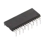
�Motion-SPM
FSB50825AB
TM
Smart Power Module (SPM®)
Features
Applications
• 250V RDS(on)=0.45Ω( max) 3-phase FRFET inverter including
high voltage integrated circuit (HVIC)
• Three-phase inverter driver for small power ac motor drives
General Description
• 3 divided negative dc-link terminals for inverter current sensing applications
FSB50825AB is a tiny smart power module (SPM®) based on
FRFET technology as a compact inverter solution for small
power motor drive applications such as fan motors and water
suppliers. It is composed of 6 fast-recovery MOSFET (FRFET),
and 3 half-bridge HVICs for FRFET gate driving. FSB50825AB
provides low electromagnetic interference (EMI) characteristics
with optimized switching speed. Moreover, since it employs
FRFET as a power switch, it has much better ruggedness and
larger safe operation area (SOA) than that of an IGBT-based
power module or one-chip solution. The package is optimized
for the thermal performance and compactness for the use in the
built-in motor application and any other application where the
assembly space is concerned. FSB50825AB is the best
solution for the compact inverter providing the energy efficiency,
compactness, and low electromagnetic interference.
• HVIC for gate driving and undervoltage protection
• Optimized for low electromagnetic interference
• Isolation voltage rating of 1500Vrms for 1min.
• HVIC temperature sensing
• Embedded bootstrap diode in the package
• RoHS compliant
©2012 Fairchild Semiconductor Corporation
FSB50825AB Rev. 1.1
1
www.fairchildsemi.com
FSB50825AB Smart Power Module (SPM®)
May 2016
�Inverter Part (Each FRFET Unless Otherwise Specified)
Symbol
Parameter
Conditions
Rating
Units
250
V
VPN
DC Link Input Voltage,
Drain-source Voltage of each FRFET
*ID25
Each FRFET Drain Current, Continuous
TC = 25°C
3.6
A
*ID80
Each FRFET Drain Current, Continuous
TC = 80°C
2.7
A
*IDP
Each FRFET Drain Current, Peak
TC = 25°C, PW < 100μs
9
A
*IDRMS
Each FRFET Drain Current, Rms
TC = 80°C, FPWM < 20KHz
1.9
Arms
Maximum Power Dissipation
TC = 25°C, For Each FRFET
14.2
W
Rating
Units
20
V
*PD
Control Part (Each HVIC Unless Otherwise Specified)
Symbol
Parameter
Conditions
VCC
Control Supply Voltage
Applied between VCC and COM
VBS
High-side Bias Voltage
Applied between VB and VS
VIN
Input Signal Voltage
Applied between IN and COM
20
V
-0.3 ~ VCC+0.3
V
Rating
Units
250
V
Bootstrap Diode Part (Each Bootstrap diode Unless Otherwise Specified)
Symbol
VRRMB
Parameter
Conditions
Maixmum Repetitive Reverse Voltage
* IFB
Forward Current
TC = 25°C
0.5
A
* IFPB
Forward Current (Peak)
TC = 25°C, Under 1ms Pulse Width
1.5
A
Conditions
Rating
Units
Each FRFET under inverter operating condition (Note 1)
8.8
°C/W
Conditions
Rating
Units
Thermal Resistance
Symbol
RθJC
Parameter
Junction to Case Thermal Resistance
Total System
Symbol
TJ
Parameter
Operating Junction Temperature
-40 ~ 150
°C
TSTG
Storage Temperature
-40 ~ 125
°C
VISO
Isolation Voltage
1500
Vrms
60Hz, Sinusoidal, 1 minute, Connection pins to heatsink
Note:
1. For the measurement point of case temperature TC, please refer to Figure 4.
2. Marking “ * “ is calculation value or design factor.
FSB50825AB Rev. 1.1
2
www.fairchildsemi.com
FSB50825AB Smart Power Module (SPM®)
Absolute Maximum Ratings
�FSB50825AB Smart Power Module (SPM®)
Pin descriptions
Pin Number
Pin Name
Pin Description
1
COM
IC Common Supply Ground
2
VB(U)
Bias Voltage for U Phase High Side FRFET Driving
3
VCC(U)
Bias Voltage for U Phase IC and Low Side FRFET Driving
4
IN(UH)
Signal Input for U Phase High-side
5
IN(UL)
Signal Input for U Phase Low-side
6
N.C
N.C
7
VB(V)
Bias Voltage for V Phase High Side FRFET Driving
8
VCC(V)
Bias Voltage for V Phase IC and Low Side FRFET Driving
9
IN(VH)
Signal Input for V Phase High-side
10
IN(VL)
Signal Input for V Phase Low-side
11
N.C
12
VB(W)
N.C
13
VCC(W)
Bias Voltage for W Phase IC and Low Side FRFET Driving
14
IN(WH)
Signal Input for W Phase High-side
15
IN(WL)
Signal Input for W Phase Low-side
16
Vts
Bias Voltage for W Phase High Side FRFET Driving
Output for HVIC temperature sensing
17
P
18
U, VS(U)
Positive DC–Link Input
19
NU
Negative DC–Link Input for U Phase
20
NV
Negative DC–Link Input for V Phase
21
V, VS(V)
22
NW
23
W, VS(W)
Output for U Phase & Bias Voltage Ground for High Side FRFET Driving
Output for V Phase & Bias Voltage Ground for High Side FRFET Driving
Negative DC–Link Input for W Phase
Output for W Phase & Bias Voltage Ground for High Side FRFET Driving
(1) COM
(17) P
(2) VB(U)
(3) V CC(U)
VCC
VB
(4) IN (UH)
HIN
HO
(5) IN (UL)
LIN
VS
COM
LO
(18) U, V S(U)
(6) N.C
(19) N U
(7) VB(V)
(8) VCC(V)
VCC
VB
(9) IN (VH)
HIN
HO
(10) IN (VL)
LIN
VS
COM
LO
(13) V CC(W)
VCC
VB
(14) IN (WH)
HIN
HO
LIN
VS
COM
LO
(20) N V
(21) V, VS(V)
(11) N.C
(12) V B(W)
(15) IN (WL)
(16) Vts
(22) N W
(23) W, V S(W)
Vts
Note:
Source terminal of each low-side MOSFET is not connected to supply ground or bias voltage ground inside SPM®. External connections should be made as indicated in Figure 3
Figure 1. Pin Configuration and Internal Block Diagram (Bottom View)
FSB50825AB Rev. 1.1
3
www.fairchildsemi.com
�Inverter Part (Each FRFET Unless Otherwise Specified)
Symbol
BVDSS
Parameter
Conditions
Drain-Source Breakdown
VIN= 0V, ID = 1mA (Note 1)
Voltage
Min Typ Max Units
250
-
-
V
IDSS
Zero Gate Voltage
Drain Current
VIN= 0V, VDS = 250V
-
-
1
mA
RDS(on)
Static Drain-Source
On-Resistance
VCC = VBS = 15V, VIN = 5V, ID = 2A
-
0.33
0.45
Ω
VSD
Drain-Source Diode
Forward Voltage
VCC = VBS = 15V, VIN = 0V, ID = -2A
-
-
1.2
V
-
950
-
ns
-
520
-
ns
Switching Times
VPN = 150V, VCC = VBS = 15V, ID = 2A
VIN = 0V ↔5V, Inductive load L=3mH
High- and low-side FRFET switching
(Note 2)
-
140
-
ns
-
100
-
μJ
-
10
-
μJ
tON
tOFF
trr
EON
EOFF
RBSOA
V = 200V, VCC = VBS = 15V, ID = IDP, VDS=BVDSS,
Reverse-bias Safe Oper- PN
TJ = 150°C
ating Area
High- and low-side FRFET switching (Note 3)
Full Square
Control Part (Each HVIC Unless Otherwise Specified)
Symbol
Parameter
Conditions
Min Typ Max Units
IQCC
Quiescent VCC Current
VCC=15V, VIN=0V
Applied between VCC and COM
-
-
200
μA
IQBS
Quiescent VBS Current
VBS=15V, VIN=0V
Applied between VB(U)-U,
VB(V)-V, VB(W)-W
-
-
100
μA
UVCCD
Low-side Undervoltage
Protection (Figure 8)
VCC Undervoltage Protection Detection Level
7.4
8.0
9.4
V
VCC Undervoltage Protection Reset Level
8.0
8.9
9.8
V
High-side Undervoltage
Protection (Figure 9)
VBS Undervoltage Protection Detection Level
7.4
8.0
9.4
V
VBS Undervoltage Protection Reset Level
8.0
8.9
9.8
V
600
790
980
mV
-
-
2.9
V
0.8
-
-
V
UVCCR
UVBSD
UVBSR
Vts
HVIC Temperature sensing voltage output
VCC=15V, THVIC=25°C(Note 4)
VIH
ON Threshold Voltage
Logic High Level
VIL
OFF Threshold Voltage
Logic Low Level
Applied between IN and COM
Bootstrap Diode Part (Each Bootstrap diode Unless Otherwise Specified)
Symbol
Parameter
Conditions
Min Typ Max Units
VFB
Forward Voltage
IF = 0.1A, TC = 25°C(Note 5)
-
2.5
-
V
trrB
Reverse Recovery Time
IF = 0.1A, TC = 25°C
-
80
-
ns
Note:
1. BVDSS is the absolute maximum voltage rating between drain and source terminal of each FRFET inside SPM®. VPN should be sufficiently less than this value considering the
effect of the stray inductance so that VDS should not exceed BVDSS in any case.
2. tON and tOFF include the propagation delay time of the internal drive IC. Listed values are measured at the laboratory test condition, and they can be different according to the
field applcations due to the effect of different printed circuit boards and wirings. Please see Figure 6 for the switching time definition with the switching test circuit of Figure 7.
3. The peak current and voltage of each FRFET during the switching operation should be included in the safe operating area (SOA). Please see Figure 7 for the RBSOA test circuit that is same as the switching test circuit.
4. Vts is only for sensing temperature of module and cannot shutdown MOSFETs automatically.
5. Built in bootstrap diode includes around 15 Ω resistance characteristic. Please refer to Figure 2.
FSB50825AB Rev. 1.1
4
www.fairchildsemi.com
FSB50825AB Smart Power Module (SPM®)
Electrical Characteristics (TJ = 25°C, VCC=VBS=15V Unless Otherwise Specified)
�Symbol
Parameter
Value
Conditions
Units
Min.
Typ.
Max.
-
150
200
V
VPN
Supply Voltage
Applied between P and N
VCC
Control Supply Voltage
Applied between VCC and COM
12
13.5
15
V
VBS
High-side Bias Voltage
Applied between VB and VS
12
13.5
15
V
3.0
-
VCC
V
0
-
0.6
V
1.0
-
-
μs
-
15
-
kHz
VIN(ON)
Input ON Threshold Voltage
VIN(OFF)
Input OFF Threshold Voltage
Applied between IN and COM
tdead
Blanking Time for Preventing
VCC=VBS=12 ~ 15V, TJ ≤ 150°C
Arm-short
fPWM
PWM Switching Frequency
TJ ≤ 150°C
Package Marking & Ordering Information
Device Marking
Device
Package
Reel Size
Packing Type
Quantity
FSB50825AB
FSB50825AB
SPM23DD-21L
-
-
15
Built in Bootstrap Diode VF-IF Characteristic
1.0
0.9
0.8
0.7
IF [A]
0.6
0.5
0.4
0.3
0.2
0.1
0.0
0
1
2
3
4
5
6
7
8
VF [V]
9
10
11
12
13
14
15
Tc=25°C
Figure 2. Built in Bootstrap Diode Characteristics(typ.)
FSB50825AB Rev. 1.1
5
www.fairchildsemi.com
FSB50825AB Smart Power Module (SPM®)
Recommended Operating Condition
�15V
Line
C1
* Example circuit : W phase
VDC
P
Micom
R5
C5
VCC
VB
HIN
HO
LIN
VS
COM
LO
V
C2
C4
LIN
Output
Note
0
0
Z
Both FRFET Off
0
1
0
Low side FRFET On
C3
1
0
VDC
High side FRFET On
1
1
Forbidden
Shoot through
Open
Open
Z
Same as (0,0)
R3
N
Vts
10μF
HIN
Inverter
Output
One Leg Diagram of SPM
* Example of bootstrap paramters
:
C1 = C2 =1μF ceramic capacitor
Note:
1. Parameters for bootsrap circuit elements are dependent on PWM algorithm. For 15 kHz of switching frequency, typical example of parameters is shown above.
2. RC coupling(R5 and C5) and C4 at each input of SPM® and Micom (indicated as dotted lines) may be used to prevent improper signal due to surge noise.
3. Bold lines should be short and thick in PCB pattern to have small stray inductance of circuit, which results in the reduction of surge voltage. Bypass capacitors such as C1, C2
and C3 should have good high-frequencycharacteristics to absorb high-frequency ripple current.
Figure 3. Recommended CPU Interface and Bootstrap Circuit with Parameters
Note:
Attach the thermocouple on top of the heatsink-side of SPM® (between SPM® and heatsink if applied) to get the correct temperature measurement.
Figure 4. Case Temperature Measurement
3.5
3.0
VTS [V]
2.5
2.0
1.5
1.0
0.5
20
40
60
80
100
120
140
160
THVIC [deg]
Figure 5. Temperature profile of Vts(typ.)
FSB50825AB Rev. 1.1
6
www.fairchildsemi.com
FSB50825AB Smart Power Module (SPM®)
These values depend on PWM
control algorithm
�FSB50825AB Smart Power Module (SPM®)
VIN
VIN
Irr
120% of ID
100% of ID
VDS
ID
10% of ID
ID
VDS
tON
trr
tOFF
(a) Turn-on
(b) Turn-off
Figure 6. Switching Time Definition
C BS
VCC
ID
VCC
VB
HIN
HO
LIN
VS
COM
LO
L
VDC
+
V DS
-
Vts
One-leg Diagram of SPM
Figure 7. Switching and RBSOA(Single-pulse) Test Circuit (Low-side)
Input Signal
UV Protection
Status
Low-side Supply, VCC
RESET
DETECTION
RESET
UVCCR
UVCCD
MOSFET Current
Figure 8. Undervoltage Protection (Low-side)
Input Signal
UV Protection
Status
High-side Supply, VBS
RESET
DETECTION
RESET
UVBSR
UVBSD
MOSFET Current
Figure 9. Undervoltage Protection (High-side)
FSB50825AB Rev. 1.1
7
www.fairchildsemi.com
�(1 ) COM
(17) P
(2 ) VB(U)
(3 ) VCC(U)
R5
(4 ) IN(UH)
(5 ) IN(UL)
C5
C2
(6 ) N.C
VCC
VB
HIN
HO
LIN
VS
COM
LO
(18 ) U , VS(U)
C3
(19 ) NU
(7 ) VB(V)
(8 ) VCC(V)
(9 ) IN(VH)
Micom
(10 ) IN(VL)
(11 ) N.C
VDC
VCC
VB
HIN
HO
LIN
VS
COM
LO
VCC
VB
HIN
HO
LIN
VS
COM
LO
(20 ) NV
(21 ) V , VS(V)
M
(12 ) VB(W)
(13 ) VCC(W)
(14 ) IN( WH)
(15 ) IN(WL)
(16 ) VTS
(22) NW
(23) W , VS(W)
VTS
C4
For current sensing and protection
15- V
Supply
R4
C6
R3
Note:
1. About pin position, refer to Figure 2.
2. RC coupling(R5 and C5, R4 and C6) and C4 at each input of SPM® and Micom are useful to prevent improper input signal caused by surge noise.
3. The voltage drop across R3 affects the low side switching performance and the bootstrap characteristics since it is placed between COM and the source terminal of the low side
MOSFET. For this reason, the voltage drop across R3 should be less than 1V in the steady-state.
4. Ground wires and output terminals, should be thick and short in order to avoid surge voltage and malfunction of HVIC.
5. All the filter capacitors shoud be connected close to SPM®, and they should have good characteristics for rejecting high-frequency ripple current.
Figure 10. Example of Application Circuit
FSB50825AB Rev. 1.1
8
www.fairchildsemi.com
FSB50825AB Smart Power Module (SPM®)
C1
�FSB50825AB Smart Power Module (SPM®)
Detailed Package Outline Drawings
FSB50825AB Rev. 1.1
9
www.fairchildsemi.com
�OPTOPLANAR®
F-PFS¥
FRFET®
SM
Global Power Resource
GreenBridge¥
Green FPS¥
Green FPS¥ e-Series¥
Gmax¥
GTO¥
IntelliMAX¥
ISOPLANAR¥
Making Small Speakers Sound Louder
and Better™
MegaBuck¥
MICROCOUPLER¥
MicroFET¥
MicroPak¥
MicroPak2¥
MillerDrive¥
MotionMax¥
MotionGrid®
MTi®
MTx®
MVN®
mWSaver®
OptoHiT¥
OPTOLOGIC®
AccuPower¥
AttitudeEngine™
Awinda®
AX-CAP®*
BitSiC¥
Build it Now¥
CorePLUS¥
CorePOWER¥
CROSSVOLT¥
CTL¥
Current Transfer Logic¥
DEUXPEED®
Dual Cool™
EcoSPARK®
EfficientMax¥
ESBC¥
®
®
Fairchild
Fairchild Semiconductor®
FACT Quiet Series¥
FACT®
FastvCore¥
FETBench¥
FPS¥
®
Power Supply WebDesigner¥
PowerTrench®
PowerXS™
Programmable Active Droop¥
QFET®
QS¥
Quiet Series¥
RapidConfigure¥
¥
Saving our world, 1mW/W/kW at a time™
SignalWise¥
SmartMax¥
SMART START¥
Solutions for Your Success¥
SPM®
STEALTH¥
SuperFET®
SuperSOT¥-3
SuperSOT¥-6
SuperSOT¥-8
SupreMOS®
SyncFET¥
Sync-Lock™
®*
TinyBoost®
TinyBuck®
TinyCalc¥
TinyLogic®
TINYOPTO¥
TinyPower¥
TinyPWM¥
TinyWire¥
TranSiC¥
TriFault Detect¥
TRUECURRENT®*
PSerDes¥
UHC®
Ultra FRFET¥
UniFET¥
VCX¥
VisualMax¥
VoltagePlus¥
XS™
Xsens™
❺®
* Trademarks of System General Corporation, used under license by Fairchild Semiconductor.
DISCLAIMER
FAIRCHILD SEMICONDUCTOR RESERVES THE RIGHT TO MAKE CHANGES WITHOUT FURTHER NOTICE TO ANY PRODUCTS HEREIN TO IMPROVE
RELIABILITY, FUNCTION, OR DESIGN. TO OBTAIN THE LATEST, MOST UP-TO-DATE DATASHEET AND PRODUCT INFORMATION, VISIT OUR
WEBSITE AT HTTP://WWW.FAIRCHILDSEMI.COM. FAIRCHILD DOES NOT ASSUME ANY LIABILITY ARISING OUT OF THE APPLICATION OR USE OF
ANY PRODUCT OR CIRCUIT DESCRIBED HEREIN; NEITHER DOES IT CONVEY ANY LICENSE UNDER ITS PATENT RIGHTS, NOR THE RIGHTS OF
OTHERS. THESE SPECIFICATIONS DO NOT EXPAND THE TERMS OF FAIRCHILD’S WORLDWIDE TERMS AND CONDITIONS, SPECIFICALLY THE
WARRANTY THEREIN, WHICH COVERS THESE PRODUCTS.
AUTHORIZED USE
Unless otherwise specified in this data sheet, this product is a standard commercial product and is not intended for use in applications that require extraordinary
levels of quality and reliability. This product may not be used in the following applications, unless specifically approved in writing by a Fairchild officer: (1) automotive
or other transportation, (2) military/aerospace, (3) any safety critical application – including life critical medical equipment – where the failure of the Fairchild product
reasonably would be expected to result in personal injury, death or property damage. Customer’s use of this product is subject to agreement of this Authorized Use
policy. In the event of an unauthorized use of Fairchild’s product, Fairchild accepts no liability in the event of product failure. In other respects, this product shall be
subject to Fairchild’s Worldwide Terms and Conditions of Sale, unless a separate agreement has been signed by both Parties.
ANTI-COUNTERFEITING POLICY
Fairchild Semiconductor Corporation's Anti-Counterfeiting Policy. Fairchild's Anti-Counterfeiting Policy is also stated on our external website, www.fairchildsemi.com,
under Terms of Use
Counterfeiting of semiconductor parts is a growing problem in the industry. All manufacturers of semiconductor products are experiencing counterfeiting of their
parts. Customers who inadvertently purchase counterfeit parts experience many problems such as loss of brand reputation, substandard performance, failed
applications, and increased cost of production and manufacturing delays. Fairchild is taking strong measures to protect ourselves and our customers from the
proliferation of counterfeit parts. Fairchild strongly encourages customers to purchase Fairchild parts either directly from Fairchild or from Authorized Fairchild
Distributors who are listed by country on our web page cited above. Products customers buy either from Fairchild directly or from Authorized Fairchild Distributors
are genuine parts, have full traceability, meet Fairchild's quality standards for handling and storage and provide access to Fairchild's full range of up-to-date technical
and product information. Fairchild and our Authorized Distributors will stand behind all warranties and will appropriately address any warranty issues that may arise.
Fairchild will not provide any warranty coverage or other assistance for parts bought from Unauthorized Sources. Fairchild is committed to combat this global
problem and encourage our customers to do their part in stopping this practice by buying direct or from authorized distributors.
PRODUCT STATUS DEFINITIONS
Definition of Terms
Datasheet Identification
Product Status
Advance Information
Formative / In Design
Preliminary
First Production
No Identification Needed
Full Production
Obsolete
Not In Production
Definition
Datasheet contains the design specifications for product development. Specifications may change
in any manner without notice.
Datasheet contains preliminary data; supplementary data will be published at a later date. Fairchild
Semiconductor reserves the right to make changes at any time without notice to improve design.
Datasheet contains final specifications. Fairchild Semiconductor reserves the right to make
changes at any time without notice to improve the design.
Datasheet contains specifications on a product that is discontinued by Fairchild Semiconductor.
The datasheet is for reference information only.
Rev. I77
© Fairchild Semiconductor Corporation
www.fairchildsemi.com
10
FSB50825AB Rev. 1.1
www.fairchildsemi.com
FSB50825AB Smart Power Module (SPM®)
TRADEMARKS
The following includes registered and unregistered trademarks and service marks, owned by Fairchild Semiconductor and/or its global subsidiaries, and is not
intended to be an exhaustive list of all such trademarks.
�ON Semiconductor and
are trademarks of Semiconductor Components Industries, LLC dba ON Semiconductor or its subsidiaries in the United States and/or other countries.
ON Semiconductor owns the rights to a number of patents, trademarks, copyrights, trade secrets, and other intellectual property. A listing of ON Semiconductor’s product/patent
coverage may be accessed at www.onsemi.com/site/pdf/Patent−Marking.pdf. ON Semiconductor reserves the right to make changes without further notice to any products herein.
ON Semiconductor makes no warranty, representation or guarantee regarding the suitability of its products for any particular purpose, nor does ON Semiconductor assume any liability
arising out of the application or use of any product or circuit, and specifically disclaims any and all liability, including without limitation special, consequential or incidental damages.
Buyer is responsible for its products and applications using ON Semiconductor products, including compliance with all laws, regulations and safety requirements or standards,
regardless of any support or applications information provided by ON Semiconductor. “Typical” parameters which may be provided in ON Semiconductor data sheets and/or
specifications can and do vary in different applications and actual performance may vary over time. All operating parameters, including “Typicals” must be validated for each customer
application by customer’s technical experts. ON Semiconductor does not convey any license under its patent rights nor the rights of others. ON Semiconductor products are not
designed, intended, or authorized for use as a critical component in life support systems or any FDA Class 3 medical devices or medical devices with a same or similar classification
in a foreign jurisdiction or any devices intended for implantation in the human body. Should Buyer purchase or use ON Semiconductor products for any such unintended or unauthorized
application, Buyer shall indemnify and hold ON Semiconductor and its officers, employees, subsidiaries, affiliates, and distributors harmless against all claims, costs, damages, and
expenses, and reasonable attorney fees arising out of, directly or indirectly, any claim of personal injury or death associated with such unintended or unauthorized use, even if such
claim alleges that ON Semiconductor was negligent regarding the design or manufacture of the part. ON Semiconductor is an Equal Opportunity/Affirmative Action Employer. This
literature is subject to all applicable copyright laws and is not for resale in any manner.
PUBLICATION ORDERING INFORMATION
LITERATURE FULFILLMENT:
Literature Distribution Center for ON Semiconductor
19521 E. 32nd Pkwy, Aurora, Colorado 80011 USA
Phone: 303−675−2175 or 800−344−3860 Toll Free USA/Canada
Fax: 303−675−2176 or 800−344−3867 Toll Free USA/Canada
Email: orderlit@onsemi.com
© Semiconductor Components Industries, LLC
N. American Technical Support: 800−282−9855 Toll Free
USA/Canada
Europe, Middle East and Africa Technical Support:
Phone: 421 33 790 2910
Japan Customer Focus Center
Phone: 81−3−5817−1050
www.onsemi.com
1
ON Semiconductor Website: www.onsemi.com
Order Literature: http://www.onsemi.com/orderlit
For additional information, please contact your local
Sales Representative
www.onsemi.com
�