Is Now Part of
To learn more about ON Semiconductor, please visit our website at
www.onsemi.com
Please note: As part of the Fairchild Semiconductor integration, some of the Fairchild orderable part numbers
will need to change in order to meet ON Semiconductor’s system requirements. Since the ON Semiconductor
product management systems do not have the ability to manage part nomenclature that utilizes an underscore
(_), the underscore (_) in the Fairchild part numbers will be changed to a dash (-). This document may contain
device numbers with an underscore (_). Please check the ON Semiconductor website to verify the updated
device numbers. The most current and up-to-date ordering information can be found at www.onsemi.com. Please
email any questions regarding the system integration to Fairchild_questions@onsemi.com.
ON Semiconductor and the ON Semiconductor logo are trademarks of Semiconductor Components Industries, LLC dba ON Semiconductor or its subsidiaries in the United States and/or other countries. ON Semiconductor owns the rights to a number
of patents, trademarks, copyrights, trade secrets, and other intellectual property. A listing of ON Semiconductor’s product/patent coverage may be accessed at www.onsemi.com/site/pdf/Patent-Marking.pdf. ON Semiconductor reserves the right
to make changes without further notice to any products herein. ON Semiconductor makes no warranty, representation or guarantee regarding the suitability of its products for any particular purpose, nor does ON Semiconductor assume any liability
arising out of the application or use of any product or circuit, and specifically disclaims any and all liability, including without limitation special, consequential or incidental damages. Buyer is responsible for its products and applications using ON
Semiconductor products, including compliance with all laws, regulations and safety requirements or standards, regardless of any support or applications information provided by ON Semiconductor. “Typical” parameters which may be provided in ON
Semiconductor data sheets and/or specifications can and do vary in different applications and actual performance may vary over time. All operating parameters, including “Typicals” must be validated for each customer application by customer’s
technical experts. ON Semiconductor does not convey any license under its patent rights nor the rights of others. ON Semiconductor products are not designed, intended, or authorized for use as a critical component in life support systems or any FDA
Class 3 medical devices or medical devices with a same or similar classification in a foreign jurisdiction or any devices intended for implantation in the human body. Should Buyer purchase or use ON Semiconductor products for any such unintended
or unauthorized application, Buyer shall indemnify and hold ON Semiconductor and its officers, employees, subsidiaries, affiliates, and distributors harmless against all claims, costs, damages, and expenses, and reasonable attorney fees arising out
of, directly or indirectly, any claim of personal injury or death associated with such unintended or unauthorized use, even if such claim alleges that ON Semiconductor was negligent regarding the design or manufacture of the part. ON Semiconductor
is an Equal Opportunity/Affirmative Action Employer. This literature is subject to all applicable copyright laws and is not for resale in any manner.
�IRLM120A
Advanced Power MOSFET
FEATURES
BVDSS = 100 V
n Avalanche Rugged Technology
RDS(on) = 0.22 Ω
n Rugged Gate Oxide Technology
n Lower Input Capacitance
ID = 2.3 A
n Improved Gate Charge
n Extended Safe Operating Area
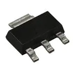
SOT-223
n Lower Leakage Current : 10 µA (Max.) @ VDS = 100V
n Lower RDS(ON) : 0.176 Ω (Typ.)
2
1
3
1. Gate 2. Drain 3. Source
Absolute Maximum Ratings
Symbol
VDSS
Characteristic
Value
Drain-to-Source Voltage
o
ID
Units
V
100
Continuous Drain Current (TC=25 C)
2.3
o
Continuous Drain Current (TC=70 C)
A
1.85
IDM
Drain Current-Pulsed
VGS
Gate-to-Source Voltage
EAS
Single Pulsed Avalanche Energy
(2)
(1)
18
A
±20
V
105
mJ
IAR
Avalanche Current
(1)
2.3
A
EAR
Repetitive Avalanche Energy
(1)
0.27
mJ
dv/dt
Peak Diode Recovery dv/dt
(3)
6.5
V/ns
o
PD
Total Power Dissipation (TC=25 C) *
Linear Derating Factor *
2.7
W
0.022
W/ C
o
Operating Junction and
TJ, TSTG
- 55 to +150
Storage Temperature Range
o
Maximum Lead Temp. for Soldering
TL
C
300
Purposes, 1/8” from case for 5-seconds
Thermal Resistance
Symbol
Characteristic
Typ.
Max.
RθJA
Junction-to-Ambient *
--
46.3
Units
o
C/W
* When mounted on the minimum pad size recommended (PCB Mount).
1
�N-CHANNEL
POWER MOSFET
IRLM120A
Electrical Characteristics (TC=25 oC unless otherwise specified)
Symbol
Characteristic
BVDSS
Drain-Source Breakdown Voltage
VGS(th)
IGSS
IDSS
RDS(on)
Breakdown Voltage Temp. Coeff.
Gate Threshold Voltage
Gate-Source Leakage , Forward
Gate-Source Leakage , Reverse
Drain-to-Source Leakage Current
Static Drain-Source
On-State Resistance
100
--
--
--
0.09
--
1.0
--
2.0
--
--
100
V
nA
See Fig 7
VDS=5V,ID=250µA
VGS=20V
VGS=-20V
--
-100
--
10
--
--
100
--
--
0.22
Ω
VGS=5V,ID=1.15A
(4)
--
VDS=40V,ID=1.15A
(4)
Forward Transconductance
--
4.6
Input Capacitance
--
340 440
Coss
Output Capacitance
--
90
115
Crss
Reverse Transfer Capacitance
--
39
50
td(on)
Turn-On Delay Time
--
5
20
Rise Time
--
10
30
Turn-Off Delay Time
--
19
50
Fall Time
--
9
30
tf
V/ C ID=250µA
--
gfs
td(off)
VGS=0V,ID=250µA
o
--
Ciss
tr
V
Test Condition
Ω
∆BV/∆TJ
Min. Typ. Max. Units
Qg
Total Gate Charge
--
10.2
15
Qgs
Gate-Source Charge
--
1.7
--
Qgd
Gate-Drain (“Miller”) Charge
--
6.0
--
µA
pF
VDS=100V
o
VDS=80V,TC=125 C
VGS=0V,VDS=25V,f =1MHz
See Fig 5
VDD=50V,ID=9.2A,
ns
RG=9 Ω
See Fig 13
(4)(5)
VDS=80V,VGS=5V,
nC
ID=9.2A
See Fig 6 & Fig 12 (4)(5)
Source-Drain Diode Ratings and Characteristics
Symbol
Characteristic
IS
Continuous Source Current
Min. Typ. Max. Units
--
--
2.3
A
Test Condition
Integral reverse pn-diode
ISM
Pulsed-Source Current
(1)
--
--
18
VSD
Diode Forward Voltage
(4)
--
--
1.5
V
TJ=25 C,IS=2.3A,VGS=0V
trr
Reverse Recovery Time
--
98
--
ns
TJ=25 C,IF=9.2A
Qrr
Reverse Recovery Charge
--
0.34
--
µC
diF/dt=100A/µs
in the MOSFET
o
o
(4)
Notes ;
① Repetitive Rating : Pulse Width Limited by Maximum Junction Temperature
② L=30mH, IAS=2.3A, VDD=25V, RG=27Ω, Starting TJ =25 oC
③ ISD < 9.2A, di/dt < 300A/μs, VDD < BVDSS , Starting TJ =25 oC
④ Pulse Test : Pulse Width = 250µs, Duty Cycle < 2%
⑤ Essentially Independent of Operating Temperature
2
�N-CHANNEL
POWER MOSFET
IRLM120A
Fig 1. Output Characteristics
Fig 2. Transfer Characteristics
VGS
ID , Drain Current [A]
101
7.0 V
6.0 V
5.5 V
5.0 V
4.5 V
4.0 V
3.5 V
Bottom : 3.0 V
ID , Drain Current [A]
Top :
100
@ Notes :
1. 250 µs Pulse Test
2. TC = 25 oC
10-1 -1
10
100
101
150 oC
100
25 oC
@ Notes :
1. VGS = 0 V
2. VDS = 40 V
3. 250 µs Pulse Test
- 55 oC
10-1
101
0
2
4
6
8
10
VDS , Drain-Source Voltage [V]
VGS , Gate-Source Voltage [V]
Fig 3. On-Resistance vs. Drain Current
Fig 4. Source-Drain Diode Forward Voltage
IDR , Reverse Drain Current [A]
Drain-Source On-Resistance
VGS = 5 V
0.3
0.2
0.1
VGS = 10 V
@ Note : TJ = 25 oC
0.0
0
10
20
30
40
101
100
@ Notes :
1. VGS = 0 V
2. 250 µs Pulse Test
150 oC
25 oC
10-1
0.4
0.6
0.8
1.0
1.2
1.4
1.6
1.8
2.0
2.2
ID , Drain Current [A]
VSD , Source-Drain Voltage [V]
Fig 5. Capacitance vs. Drain-Source Voltage
Fig 6. Gate Charge vs. Gate-Source Voltage
600
360
C iss
Ciss= Cgs+ Cgd ( Cds= shorted )
Coss= Cds+ Cgd
Crss= Cgd
C oss
240
@ Notes :
1. VGS = 0 V
2. f = 1 MHz
C rss
120
00
10
101
VDS , Drain-Source Voltage [V]
6
VDS = 20 V
VGS , Gate-Source Voltage [V]
480
Capacitance [pF]
RDS(on) , [ Ω ]
0.4
VDS = 50 V
VDS = 80 V
4
2
@ Notes : ID = 9.2 A
0
0
2
4
6
8
10
12
QG , Total Gate Charge [nC]
3
�N-CHANNEL
POWER MOSFET
IRLM120A
Fig 7. Breakdown Voltage vs. Temperature
Fig 8. On-Resistance vs. Temperature
1.1
1.0
0.9
@ Notes :
1. V = 0 V
GS
Drain-Source On-Resistance
2.5
RDS(on) , (Normalized)
BVDSS , (Normalized)
Drain-Source Breakdown Voltage
1.2
2.0
1.5
1.0
@ Notes :
1. V = 5 V
0.5
GS
2. ID = 4.6 A
2. ID = 250 µA
0.8
-75
-50
-25
0
25
50
75
100
125
150
0.0
-75
175
-50
-25
o
102
0
25
50
75
100
125
150
175
TJ , Junction Temperature [oC]
TJ , Junction Temperature [ C]
Fig 9. Max. Safe Operating Area
Fig 10. Max. Drain Current vs. Case Temperature
10
ID , Drain Current [A]
100 µs
101
1 ms
10 ms
DC
100
@ Notes :
1. TC = 25 oC
2. TJ = 150 oC
3. Single Pulse
8
6
4
2
10-1 0
10
101
0
25
102
50
100
125
150
Fig 11. Thermal Response
101
Thermal Response
75
Tc , Case Temperature [oC]
VDS , Drain-Source Voltage [V]
D=0.5
100
0.2
@ Notes :
1. Z J C (t)=3.5 o C/W Max.
0.1
0.05
10- 1
θ
2. Duty Factor, D=t1 /t2
0.02
3. TJ M -TC =PD M *Zθ J C (t)
0.01
PDM
single pulse
t1
θJC
Z (t) ,
ID , Drain Current [A]
Operation in This Area
is Limited by R DS(on)
t2
-2
10
10- 5
10- 4
10- 3
10- 2
10- 1
t 1 , Square Wave Pulse Duration
100
101
[sec]
4
�N-CHANNEL
POWER MOSFET
IRLM120A
Fig 12. Gate Charge Test Circuit & Waveform
* Current Regulator ”
VGS
Same Type
as DUT
50KΩ
Qg
200nF
12V
10V
300nF
VDS
Qgs
VGS
Qgd
DUT
3mA
R1
R2
Current Sampling (IG)
Resistor
Current Sampling (ID)
Resistor
Charge
Fig 13. Resistive Switching Test Circuit & Waveforms
RL
Vout
Vout
90%
VDD
Vin
( 0.5 rated VDS )
RG
DUT
Vin
10%
10V
td(on)
tr
td(off)
t on
tf
t off
Fig 14. Unclamped Inductive Switching Test Circuit & Waveforms
BVDSS
1
EAS = ---- LL IAS2 -------------------2
BVDSS -- VDD
LL
VDS
Vary tp to obtain
required peak ID
BVDSS
IAS
ID
RG
C
DUT
ID (t)
VDD
VDS (t)
VDD
5V
tp
tp
Time
5
�N-CHANNEL
POWER MOSFET
IRLM120A
Fig 15. Peak Diode Recovery dv/dt Test Circuit & Waveforms
DUT
+
VDS
--
IS
L
Driver
VGS
RG
VGS
VGS
( Driver )
Same Type
as DUT
VDD
• dv/dt controlled by "RG"
• IS controlled by Duty Factor "D"
Gate Pulse Width
D = -------------------------Gate Pulse Period
10V
IFM , Body Diode Forward Current
IS
( DUT )
di/dt
IRM
Body Diode Reverse Current
VDS
( DUT )
Body Diode Recovery dv/dt
Vf
VDD
Body Diode
Forward Voltage Drop
6
�TRADEMARKS
The following are registered and unregistered trademarks Fairchild Semiconductor owns or is authorized to use and is
not intended to be an exhaustive list of all such trademarks.
ACEx™
Bottomless™
CoolFET™
CROSSVOLT™
DenseTrench™
DOME™
EcoSPARK™
E2CMOSTM
EnSignaTM
FACT™
FACT Quiet Series™
FAST
FASTr™
FRFET™
GlobalOptoisolator™
GTO™
HiSeC™
ISOPLANAR™
LittleFET™
MicroFET™
MICROWIRE™
OPTOLOGIC™
OPTOPLANAR™
PACMAN™
POP™
Power247™
PowerTrench
QFET™
QS™
QT Optoelectronics™
Quiet Series™
SILENT SWITCHER
SMART START™
STAR*POWER™
Stealth™
SuperSOT™-3
SuperSOT™-6
SuperSOT™-8
SyncFET™
TinyLogic™
TruTranslation™
UHC™
UltraFET
VCX™
STAR*POWER is used under license
DISCLAIMER
FAIRCHILD SEMICONDUCTOR RESERVES THE RIGHT TO MAKE CHANGES WITHOUT FURTHER
NOTICE TO ANY PRODUCTS HEREIN TO IMPROVE RELIABILITY, FUNCTION OR DESIGN. FAIRCHILD
DOES NOT ASSUME ANY LIABILITY ARISING OUT OF THE APPLICATION OR USE OF ANY PRODUCT
OR CIRCUIT DESCRIBED HEREIN; NEITHER DOES IT CONVEY ANY LICENSE UNDER ITS PATENT
RIGHTS, NOR THE RIGHTS OF OTHERS.
LIFE SUPPORT POLICY
FAIRCHILD’S PRODUCTS ARE NOT AUTHORIZED FOR USE AS CRITICAL COMPONENTS IN LIFE SUPPORT
DEVICES OR SYSTEMS WITHOUT THE EXPRESS WRITTEN APPROVAL OF FAIRCHILD SEMICONDUCTOR CORPORATION.
As used herein:
2. A critical component is any component of a life
1. Life support devices or systems are devices or
support device or system whose failure to perform can
systems which, (a) are intended for surgical implant into
be reasonably expected to cause the failure of the life
the body, or (b) support or sustain life, or (c) whose
support device or system, or to affect its safety or
failure to perform when properly used in accordance
with instructions for use provided in the labeling, can be
effectiveness.
reasonably expected to result in significant injury to the
user.
PRODUCT STATUS DEFINITIONS
Definition of Terms
Datasheet Identification
Product Status
Definition
Advance Information
Formative or
In Design
This datasheet contains the design specifications for
product development. Specifications may change in
any manner without notice.
Preliminary
First Production
This datasheet contains preliminary data, and
supplementary data will be published at a later date.
Fairchild Semiconductor reserves the right to make
changes at any time without notice in order to improve
design.
No Identification Needed
Full Production
This datasheet contains final specifications. Fairchild
Semiconductor reserves the right to make changes at
any time without notice in order to improve design.
Obsolete
Not In Production
This datasheet contains specifications on a product
that has been discontinued by Fairchild semiconductor.
The datasheet is printed for reference information only.
Rev. H3
�ON Semiconductor and
are trademarks of Semiconductor Components Industries, LLC dba ON Semiconductor or its subsidiaries in the United States and/or other countries.
ON Semiconductor owns the rights to a number of patents, trademarks, copyrights, trade secrets, and other intellectual property. A listing of ON Semiconductor’s product/patent
coverage may be accessed at www.onsemi.com/site/pdf/Patent−Marking.pdf. ON Semiconductor reserves the right to make changes without further notice to any products herein.
ON Semiconductor makes no warranty, representation or guarantee regarding the suitability of its products for any particular purpose, nor does ON Semiconductor assume any liability
arising out of the application or use of any product or circuit, and specifically disclaims any and all liability, including without limitation special, consequential or incidental damages.
Buyer is responsible for its products and applications using ON Semiconductor products, including compliance with all laws, regulations and safety requirements or standards,
regardless of any support or applications information provided by ON Semiconductor. “Typical” parameters which may be provided in ON Semiconductor data sheets and/or
specifications can and do vary in different applications and actual performance may vary over time. All operating parameters, including “Typicals” must be validated for each customer
application by customer’s technical experts. ON Semiconductor does not convey any license under its patent rights nor the rights of others. ON Semiconductor products are not
designed, intended, or authorized for use as a critical component in life support systems or any FDA Class 3 medical devices or medical devices with a same or similar classification
in a foreign jurisdiction or any devices intended for implantation in the human body. Should Buyer purchase or use ON Semiconductor products for any such unintended or unauthorized
application, Buyer shall indemnify and hold ON Semiconductor and its officers, employees, subsidiaries, affiliates, and distributors harmless against all claims, costs, damages, and
expenses, and reasonable attorney fees arising out of, directly or indirectly, any claim of personal injury or death associated with such unintended or unauthorized use, even if such
claim alleges that ON Semiconductor was negligent regarding the design or manufacture of the part. ON Semiconductor is an Equal Opportunity/Affirmative Action Employer. This
literature is subject to all applicable copyright laws and is not for resale in any manner.
PUBLICATION ORDERING INFORMATION
LITERATURE FULFILLMENT:
Literature Distribution Center for ON Semiconductor
19521 E. 32nd Pkwy, Aurora, Colorado 80011 USA
Phone: 303−675−2175 or 800−344−3860 Toll Free USA/Canada
Fax: 303−675−2176 or 800−344−3867 Toll Free USA/Canada
Email: orderlit@onsemi.com
© Semiconductor Components Industries, LLC
N. American Technical Support: 800−282−9855 Toll Free
USA/Canada
Europe, Middle East and Africa Technical Support:
Phone: 421 33 790 2910
Japan Customer Focus Center
Phone: 81−3−5817−1050
www.onsemi.com
1
ON Semiconductor Website: www.onsemi.com
Order Literature: http://www.onsemi.com/orderlit
For additional information, please contact your local
Sales Representative
www.onsemi.com
�