ISL9V2040D3S / ISL9V2040S3S / ISL9V2040P3
EcoSPARK 200mJ, 400V, N-Channel Ignition IGBT
General Description
Applications
The ISL9V2040D3S, ISL9V2040S3S, and ISL9V2040P3 are the
next generation ignition IGBTs that offer outstanding SCIS
capability in the space saving D-Pak (TO-252), as well as the
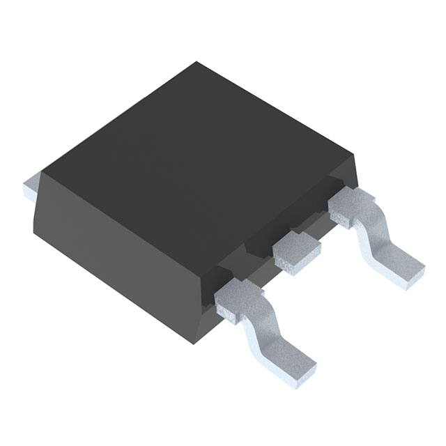
industry standard D²-Pak (TO-263) and TO-220 plastic packages.
This device is intended for use in automotive ignition circuits,
specifically as a coil driver. Internal diodes provide voltage clamping
without the need for external components.
• Automotive Ignition Coil Driver Circuits
• Coil- On Plug Applications
EcoSPARK devices can be custom made to specific clamp
voltages. Contact your nearest Fairchild sales office for more
information.
Features
• Space saving D - Pak package available
• SCIS Energy = 200mJ at TJ = 25oC
• Logic Level Gate Drive
Formerly Developmental Type 49444
Package
Symbol
COLLECTOR
JEDEC TO-252AA
D-Pak
JEDEC TO-263AB
D²-Pak
JEDEC TO-220AB
E
C
G
R1
GATE
G
G
E
R2
E
COLLECTOR
(FLANGE)
EMITTER
COLLECTOR
(FLANGE)
Device Maximum Ratings TA = 25°C unless otherwise noted
Symbol
BVCER
Parameter
Collector to Emitter Breakdown Voltage (IC = 1 mA)
Ratings
430
Units
V
BVECS
Emitter to Collector Voltage - Reverse Battery Condition (IC = 10 mA)
24
V
ESCIS25
At Starting TJ = 25°C, ISCIS = 11.5A, L = 3.0mHy
200
mJ
ESCIS150
At Starting TJ = 150°C, ISCIS = 8.9A, L = 3.0mHy
120
mJ
IC25
Collector Current Continuous, At TC = 25°C, See Fig 9
10
A
IC110
Collector Current Continuous, At TC = 110°C, See Fig 9
10
A
VGEM
Gate to Emitter Voltage Continuous
±10
V
PD
Power Dissipation Total TC = 25°C
130
W
Power Dissipation Derating TC > 25°C
0.87
W/°C
Operating Junction Temperature Range
-40 to 175
°C
Storage Junction Temperature Range
-40 to 175
°C
Max Lead Temp for Soldering (Leads at 1.6mm from Case for 10s)
300
°C
Tpkg
Max Lead Temp for Soldering (Package Body for 10s)
260
°C
ESD
Electrostatic Discharge Voltage at 100pF, 1500Ω
4
kV
TJ
TSTG
TL
©2004 Fairchild Semiconductor Corporation
ISL9V2040D3S / ISL9V2040S3S / ISL9V2040P3 Rev. B�, October 20��
ISL9V2040D3S / ISL9V2040S3S / ISL9V2040P3
October 20��
�Device Marking
V2040D
Device
ISL9V2040D3ST
Package
TO-252AA
Reel Size
330mm
Tape Width
16mm
Quantity
2500
800
V2040S
ISL9V2040S3ST
TO-263AB
330mm
24mm
V2040P
ISL9V2040P3
TO-220AB
Tube
N/A
50
V2040D
ISL9V2040D3S
TO-252AA
Tube
N/A
75
V2040S
ISL9V2040S3S
TO-263AB
Tube
N/A
50
Electrical Characteristics TA = 25°C unless otherwise noted
Symbol
Parameter
Test Conditions
Min
Typ
Max
Units
Off State Characteristics
BVCER
Collector to Emitter Breakdown Voltage
IC = 2mA, VGE = 0,
RG = 1KΩ, See Fig. 15
TJ = -40 to 150°C
370
400
430
V
BVCES
Collector to Emitter Breakdown Voltage
IC = 10mA, VGE = 0,
RG = 0, See Fig. 15
TJ = -40 to 150°C
390
420
450
V
BVECS
Emitter to Collector Breakdown Voltage
IC = -75mA, VGE = 0V,
TC = 25°C
30
-
-
V
BVGES
Gate to Emitter Breakdown Voltage
IGES = ± 2mA
Collector to Emitter Leakage Current
VCER = 250V,
RG = 1KΩ,
See Fig. 11
ICER
IECS
Emitter to Collector Leakage Current
R1
Series Gate Resistance
R2
Gate to Emitter Resistance
±12
±14
-
V
TC = 25°C
-
-
25
µA
TC = 150°C
-
-
1
mA
VEC = 24V, See TC = 25°C
Fig. 11
TC = 150°C
-
-
1
mA
-
-
40
mA
-
70
-
Ω
10K
-
26K
Ω
On State Characteristics
VCE(SAT)
Collector to Emitter Saturation Voltage
IC = 6A,
VGE = 4V
TC = 25°C,
See Fig. 3
-
1.45
1.9
V
VCE(SAT)
Collector to Emitter Saturation Voltage
IC = 10A,
VGE = 4.5V
TC = 150°C
See Fig. 4
-
1.95
2.3
V
-
12
-
nC
Dynamic Characteristics
QG(ON)
Gate Charge
IC = 10A, VCE = 12V,
VGE = 5V, See Fig. 14
VGE(TH)
Gate to Emitter Threshold Voltage
IC = 1.0mA,
VCE = VGE,
See Fig. 10
VGEP
Gate to Emitter Plateau Voltage
TC = 25°C
1.3
-
2.2
V
TC = 150°C
0.75
-
1.8
V
-
3.4
-
V
IC = 10A, VCE = 12V
Switching Characteristics
td(ON)R
triseR
td(OFF)L
tfL
SCIS
Current Turn-On Delay Time-Resistive
Current Rise Time-Resistive
Current Turn-Off Delay Time-Inductive
Current Fall Time-Inductive
Self Clamped Inductive Switching
VCE = 14V, RL = 1Ω,
VGE = 5V, RG = 1KΩ
TJ = 25°C
-
0.61
-
µs
-
2.17
-
µs
VCE = 300V, L = 500µHy,
VGE = 5V, RG = 1KΩ
TJ = 25°C, See Fig. 12
-
3.64
-
µs
-
2.36
-
µs
TJ = 25°C, L = 3.0mHy,
RG = 1KΩ, VGE = 5V, See
Fig. 1 & 2
-
-
200
mJ
TO-252, TO-263, TO-220
-
-
1.15
°C/W
Thermal Characteristics
RθJC
Thermal Resistance Junction-Case
©2004 Fairchild Semiconductor Corporation
ISL9V2040D3S / ISL9V2040S3S / ISL9V2040P3 Rev. B�, October 20��
ISL9V2040D3S / ISL9V2040S3S / ISL9V2040P3
Package Marking and Ordering Information
�20
ISCIS, INDUCTIVE SWITCHING CURRENT (A)
ISCIS, INDUCTIVE SWITCHING CURRENT (A)
20
RG = 1KΩ, VGE = 5V,Vdd = 14V
18
16
14
TJ = 25°C
12
10
TJ = 150°C
8
6
4
2
SCIS Curves valid for Vclamp Voltages of