物料型号:MC100EP140
器件简介:MC100EP140是一款三态相位频率检测器,适用于需要最小相位和频率差异锁定的锁相环应用。该器件设计有全差分内部门,可降低噪声,特别是在高速应用中。
引脚分配:文档中提供了引脚分配图,包括VCC、VEE、FB、R、U、D等引脚,其中U和D为差分上升和下降输出,R为ECL参考输入,FB为ECL反馈输入。
参数特性:典型传播延迟为500皮秒,最大频率大于2.1 GHz,具有400毫伏的高级高带宽输出摆动,传输增益在1.4 GHz时为1.0 mV/度,在1.0 GHz时为1.2 mV/度,上升和下降时间典型值为100皮秒。
功能详解:相位/频率检测器(PFD)的基本操作是“比较”一个输入信号(反馈)与一个设定的参考信号。当参考(R)和反馈(FB)输入在频率和/或相位上不相等时,差分上升(U)和下降(D)输出将提供脉冲流,这些脉冲流在减去并积分后,提供用于控制压控振荡器(VCO)的误差电压。
应用信息:有关锁相环操作和应用的更多信息可以在AND8040中找到。
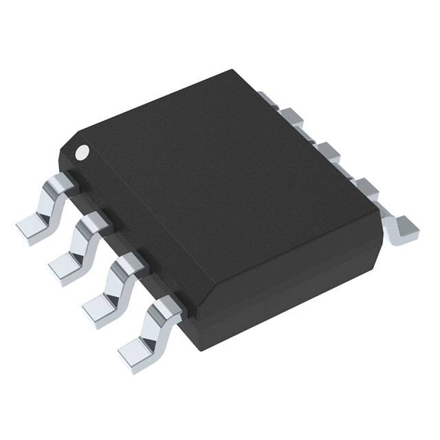
封装信息:提供SOIC-8封装,有铅和无铅两种选项。