MMBF4391LT1G, MMBF4392LT1G, MMBF4393LT1G JFET Switching Transistors
N−Channel
Features http://onsemi.com
2 SOURCE
• These Devices are Pb−Free, Halogen Free/BFR Free and are RoHS
Compliant
3 GATE
MAXIMUM RATINGS
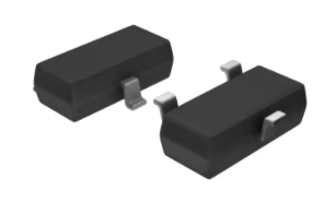
Rating Drain−Source Voltage Drain−Gate Voltage Gate−Source Voltage Forward Gate Current Symbol VDS VDG VGS IG(f) Value 30 30 30 50 Unit Vdc Vdc Vdc mAdc 1 2 Max 225 1.8 556 − 55 to +150 Unit mW mW/°C °C/W °C 6x M G G 1 6x M G = Specific Device Code = Date Code* = Pb−Free Package SOT−23 CASE 318 STYLE 10 3 1 DRAIN
THERMAL CHARACTERISTICS
Characteristic Total Device Dissipation FR− 5 Board (Note 1) TA = 25°C Derate above 25°C Thermal Resistance, Junction−to−Ambient Junction and Storage Temperature Range Symbol PD
RqJA TJ, Tstg
MARKING DIAGRAM
Stresses exceeding Maximum Ratings may damage the device. Maximum Ratings are stress ratings only. Functional operation above the Recommended Operating Conditions is not implied. Extended exposure to stresses above the Recommended Operating Conditions may affect device reliability. 1. FR− 5 = 1.0 � 0.75 � 0.062 in.
(Note: Microdot may be in either location) *Date Code orientation and/or overbar may vary depending upon manufacturing location.
DEVICE MARKING INFORMATION
See general marking information in the device marking section on page 2 of this data sheet.
ORDERING INFORMATION
See detailed ordering and shipping information in the package dimensions section on page 2 of this data sheet.
© Semiconductor Components Industries, LLC, 2009
October, 2009 − Rev. 7
1
Publication Order Number: MMBF4391LT1/D
�MMBF4391LT1G, MMBF4392LT1G, MMBF4393LT1G
ELECTRICAL CHARACTERISTICS (TA = 25°C unless otherwise noted)
Characteristic OFF CHARACTERISTICS Gate−Source Breakdown Voltage (IG = 1.0 mAdc, VDS = 0) Gate Reverse Current (VGS = 15 Vdc, VDS = 0, TA = 25°C) (VGS = 15 Vdc, VDS = 0, TA = 100°C) Gate−Source Cutoff Voltage (VDS = 15 Vdc, ID = 10 nAdc) MMBF4391LT1 MMBF4392LT1 MMBF4393LT1 V(BR)GSS IGSS 30 − Vdc Symbol Min Max Unit
− − −4.0 −2.0 −0.5 − −
1.0 0.20 −10 −5.0 −3.0 1.0 1.0
nAdc mAdc Vdc
VGS(off)
Off−State Drain Current (VDS = 15 Vdc, VGS = −12 Vdc) (VDS = 15 Vdc, VGS = −12 Vdc, TA = 100°C) ON CHARACTERISTICS Zero−Gate−Voltage Drain Current (VDS = 15 Vdc, VGS = 0) MMBF4391LT1 MMBF4392LT1 MMBF4393LT1 MMBF4391LT1 MMBF4392LT1 MMBF4393LT1 MMBF4391LT1 MMBF4392LT1 MMBF4393LT1
ID(off)
nAdc mAdc mAdc
IDSS
50 25 5.0 − − − − − −
150 75 30 0.4 0.4 0.4 30 60 100
Drain−Source On−Voltage (ID = 12 mAdc, VGS = 0) (ID = 6.0 mAdc, VGS = 0) (ID = 3.0 mAdc, VGS = 0) Static Drain−Source On−Resistance (ID = 1.0 mAdc, VGS = 0)
VDS(on)
Vdc
rDS(on)
W
SMALL− SIGNAL CHARACTERISTICS Input Capacitance (VDS = 0 Vdc, VGS = −15 Vdc, f = 1.0 MHz) Reverse Transfer Capacitance (VDS = 0 Vdc, VGS = −12 Vdc, f = 1.0 MHz) Ciss Crss − − 14 3.5 pF pF
ORDERING INFORMATION
Device MMBF4391LT1G MMBF4392LT1G MMBF4393LT1G Marking 6J 6K 6G Package SOT−23 (Pb−Free) SOT−23 (Pb−Free) SOT−23 (Pb−Free) 3000 / Tape & Reel Shipping†
†For information on tape and reel specifications, including part orientation and tape sizes, please refer to our Tape and Reel Packaging Specifications Brochure, BRD8011/D.
http://onsemi.com
2
�MMBF4391LT1G, MMBF4392LT1G, MMBF4393LT1G
TYPICAL CHARACTERISTICS
1000 t d(on) , TURN-ON DELAY TIME (ns) 500 200 100 50 20 10 5.0 2.0 1.0 0.5 0.7 1.0
RK = 0 RK = RD' TJ = 25°C MMBF4391 MMBF4392 MMBF4393 VGS(off) = 12 V = 7.0 V = 5.0 V
1000 500 200 t r , RISE TIME (ns) 100 50 20 10 5.0 2.0 1.0 0.5 0.7 1.0
RK = 0 RK = RD'
TJ = 25°C MMBF4391 MMBF4392 MMBF4393 VGS(off) = 12 V = 7.0 V = 5.0 V
2.0 3.0 5.0 7.0 10 ID, DRAIN CURRENT (mA)
20
30
50
2.0 3.0 5.0 7.0 10 ID, DRAIN CURRENT (mA)
20
30
50
Figure 1. Turn−On Delay Time
Figure 2. Rise Time
1000 500 t f , FALL TIME (ns) 200 100 50 20 10 5.0 2.0 1.0 0.5 0.7 1.0
RK = 0
t d(off) , TURN-OFF DELAY TIME (ns)
1000 500 200 100 50 20 10 5.0 2.0 1.0 0.5 0.7 1.0
RK = 0 RK = RD'
TJ = 25°C MMBF4391 MMBF4392 MMBF4393 VGS(off) = 12 V = 7.0 V = 5.0 V
RK = RD'
TJ = 25°C MMBF4391 MMBF4392 MMBF4393 VGS(off) = 12 V = 7.0 V = 5.0 V
2.0 3.0 5.0 7.0 10 ID, DRAIN CURRENT (mA)
20
30
50
2.0 3.0 5.0 7.0 10 20 ID, DRAIN CURRENT (mA)
30
50
Figure 3. Turn−Off Delay Time
Figure 4. Fall Time
http://onsemi.com
3
�MMBF4391LT1G, MMBF4392LT1G, MMBF4393LT1G
NOTE 1
VDD RD
SET VDS(off) = 10 V INPUT
RK RGG 50 W VGG
RT
OUTPUT
RGEN 50 W VGEN
INPUT PULSE tr ≤ 0.25 ns tf ≤ 0.5 ns PULSE WIDTH = 2.0 ms DUTY CYCLE ≤ 2.0%
50 W
RGG > RK RD' = RD(RT + 50) RD + RT + 50
Figure 5. Switching Time Test Circuit
The switching characteristics shown above were measured using a test circuit similar to Figure 5. At the beginning of the switching interval, the gate voltage is at Gate Supply Voltage (−VGG). The Drain−Source Voltage (VDS) is slightly lower than Drain Supply Voltage (VDD) due to the voltage divider. Thus Reverse Transfer Capacitance (Crss) of Gate−Drain Capacitance (Cgd) is charged to VGG + VDS. During the turn−on interval, Gate−Source Capacitance (Cgs) discharges through the series combination of RGen and RK. Cgd must discharge to VDS(on) through RG and RK in series with the parallel combination of effective load impedance (R’D) and Drain−Source Resistance (rDS). During the turn−off, this charge flow is reversed. Predicting turn−on time is somewhat difficult as the channel resistance rDS is a function of the gate−source voltage. While Cgs discharges, VGS approaches zero and rDS decreases. Since Cgd discharges through rDS, turn−on time is non−linear. During turn−off, the situation is reversed with rDS increasing as Cgd charges. The above switching curves show two impedance conditions; 1) RK is equal to RD’ which simulates the switching behavior of cascaded stages where the driving source impedance is normally the load impedance of the previous stage, and 2) RK = 0 (low impedance) the driving source impedance is that of the generator.
V fs , FORWARD TRANSFER ADMITTANCE (mmhos)
20
MMBF4392
15
MMBF4391
10 C, CAPACITANCE (pF) 7.0 5.0 3.0 2.0 1.5 1.0 0.03 0.05 0.1
Cgs
10
MMBF4393
7.0 5.0 3.0 2.0 0.5 0.7 1.0 2.0 3.0 5.0 7.0 10 20 30 50
Tchannel = 25°C VDS = 15 V
Cgd Tchannel = 25°C (Cds is negligible
0.3 0.5
1.0
3.0 5.0
10
30
ID, DRAIN CURRENT (mA)
VR, REVERSE VOLTAGE (VOLTS)
Figure 6. Typical Forward Transfer Admittance
r DS(on), DRAIN-SOURCE ON-STATE RESISTANCE (NORMALIZED) 200 r DS(on), DRAIN-SOURCE ON-STATE RESISTANCE (OHMS)
IDSS 25 mA = 10 160 mA 50 mA 75 mA 100 mA 125 mA
Figure 7. Typical Capacitance
2.0 1.8 1.6 1.4 1.2 1.0 0.8 0.6 0.4 -70 -40 -10 20 50 80 110 140 170
ID = 1.0 mA VGS = 0
120 80 40
Tchannel = 25°C
0
0
1.0
2.0 3.0 5.0 4.0 6.0 7.0 VGS, GATE-SOURCE VOLTAGE (VOLTS)
8.0
Tchannel, CHANNEL TEMPERATURE (°C)
Figure 8. Effect of Gate−Source Voltage on Drain−Source Resistance
Figure 9. Effect of Temperature on Drain−Source On−State Resistance
http://onsemi.com
4
�MMBF4391LT1G, MMBF4392LT1G, MMBF4393LT1G
NOTE 2
r DS(on) , DRAIN-SOURCE ON-STATE RESISTANCE (OHMS) 100 90 80 70 60 50 40 30 20 10 0
Tchannel = 25°C
10 9.0 8.0 7.0 6.0
VGS(off)
rDS(on) @ VGS = 0
5.0 4.0
3.0 2.0 1.0 0 10 20 30 40 50 60 70 80 90 100 110 120 130 140 150 IDSS, ZERO-GATE VOLTAGE DRAIN CURRENT (mA)
Figure 10. Effect of IDSS on Drain−Source Resistance and Gate−Source Voltage
The Zero−Gate−Voltage Drain Current (IDSS) is the principle determinant of other J−FET characteristics. Figure 10 shows the relationship of Gate−Source Off Voltage (VGS(off)) and Drain−Source On Resistance (rDS(on)) to IDSS. Most of the devices will be within ±10% of the values shown in Figure 10. This data will be useful in predicting the characteristic variations for a given part number. For example: Unknown rDS(on) and VGS range for an MMBF4392 The electrical characteristics table indicates that an MMBF4392 has an IDSS range of 25 to 75 mA. Figure 10 shows rDS(on) = 52 W for IDSS = 25 mA and 30 W for IDSS = 75 mA. The corresponding VGS values are 2.2 V and 4.8 V.
http://onsemi.com
5
V GS , GATE-SOURCE VOLTAGE (VOLTS)
�MMBF4391LT1G, MMBF4392LT1G, MMBF4393LT1G
PACKAGE DIMENSIONS
SOT−23 (TO−236) CASE 318−08 ISSUE AN
D
SEE VIEW C 3 NOTES: 1. DIMENSIONING AND TOLERANCING PER ANSI Y14.5M, 1982. 2. CONTROLLING DIMENSION: INCH. 3. MAXIMUM LEAD THICKNESS INCLUDES LEAD FINISH THICKNESS. MINIMUM LEAD THICKNESS IS THE MINIMUM THICKNESS OF BASE MATERIAL. 4. 318−01 THRU −07 AND −09 OBSOLETE, NEW STANDARD 318−08. MILLIMETERS NOM MAX 1.00 1.11 0.06 0.10 0.44 0.50 0.13 0.18 2.90 3.04 1.30 1.40 1.90 2.04 0.20 0.30 0.54 0.69 2.40 2.64 INCHES NOM 0.040 0.002 0.018 0.005 0.114 0.051 0.075 0.008 0.021 0.094
E
1 2
HE c e b q 0.25
A A1 L L1 VIEW C
DIM A A1 b c D E e L L1 HE
MIN 0.89 0.01 0.37 0.09 2.80 1.20 1.78 0.10 0.35 2.10
MIN 0.035 0.001 0.015 0.003 0.110 0.047 0.070 0.004 0.014 0.083
MAX 0.044 0.004 0.020 0.007 0.120 0.055 0.081 0.012 0.029 0.104
STYLE 10: PIN 1. DRAIN 2. SOURCE 3. GATE
SOLDERING FOOTPRINT*
0.95 0.037 0.95 0.037
2.0 0.079 0.9 0.035
SCALE 10:1
0.8 0.031
mm inches
*For additional information on our Pb−Free strategy and soldering details, please download the ON Semiconductor Soldering and Mounting Techniques Reference Manual, SOLDERRM/D.
ON Semiconductor and are registered trademarks of Semiconductor Components Industries, LLC (SCILLC). SCILLC reserves the right to make changes without further notice to any products herein. SCILLC makes no warranty, representation or guarantee regarding the suitability of its products for any particular purpose, nor does SCILLC assume any liability arising out of the application or use of any product or circuit, and specifically disclaims any and all liability, including without limitation special, consequential or incidental damages. “Typical” parameters which may be provided in SCILLC data sheets and/or specifications can and do vary in different applications and actual performance may vary over time. All operating parameters, including “Typicals” must be validated for each customer application by customer’s technical experts. SCILLC does not convey any license under its patent rights nor the rights of others. SCILLC products are not designed, intended, or authorized for use as components in systems intended for surgical implant into the body, or other applications intended to support or sustain life, or for any other application in which the failure of the SCILLC product could create a situation where personal injury or death may occur. Should Buyer purchase or use SCILLC products for any such unintended or unauthorized application, Buyer shall indemnify and hold SCILLC and its officers, employees, subsidiaries, affiliates, and distributors harmless against all claims, costs, damages, and expenses, and reasonable attorney fees arising out of, directly or indirectly, any claim of personal injury or death associated with such unintended or unauthorized use, even if such claim alleges that SCILLC was negligent regarding the design or manufacture of the part. SCILLC is an Equal Opportunity/Affirmative Action Employer. This literature is subject to all applicable copyright laws and is not for resale in any manner.
PUBLICATION ORDERING INFORMATION
LITERATURE FULFILLMENT: Literature Distribution Center for ON Semiconductor P.O. Box 5163, Denver, Colorado 80217 USA Phone: 303−675−2175 or 800−344−3860 Toll Free USA/Canada Fax: 303−675−2176 or 800−344−3867 Toll Free USA/Canada Email: orderlit@onsemi.com N. American Technical Support: 800−282−9855 Toll Free USA/Canada Europe, Middle East and Africa Technical Support: Phone: 421 33 790 2910 Japan Customer Focus Center Phone: 81−3−5773−3850 ON Semiconductor Website: www.onsemi.com Order Literature: http://www.onsemi.com/orderlit For additional information, please contact your local Sales Representative
http://onsemi.com
6
MMBF4391LT1/D
�


 工商网监
湘ICP备2023018690号
工商网监
湘ICP备2023018690号
