MMPQ3906
Preferred Device
Quad Amplifier/Switch Transistor
PNP Silicon
http://onsemi.com
MAXIMUM RATINGS
Rating Collector − Emitter Voltage Collector − Base Voltage Emitter − Base Voltage Collector Current − Continuous Symbol VCEO VCB VEB IC Value −40 −40 −5.0 −200 Each Transistor Power Dissipation @ TA = 25°C Derate above 25°C Power Dissipation @ TC = 25°C Derate above 25°C PD PD 200 3.2 0.66 5.3 Four Transistors Equal Power Power Dissipation @ TA = 25°C Derate above 25°C Power Dissipation @ TC = 25°C Derate above 25°C Operating and Storage Junction Temperature Range PD PD TJ, Tstg 800 6.4 1.92 15.4 −55 to +150 mW mW/°C Watts mW/°C °C mW mW/°C Watts mW/°C
16
1
16 15 14 13 12 11 10 9
Unit Vdc Vdc Vdc mAdc
2 3 4 5 6 7 8
1
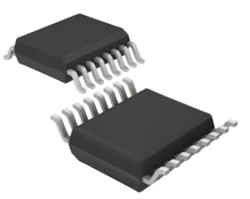
SO−16 CASE 751B STYLE 4
MARKING DIAGRAM
MMPQ3906 AWLYWW
MMPQ3906 = Specific Device Code A = Assembly Location WL = Wafer Lot Y = Year WW = Work Week
ORDERING INFORMATION
Device MMPQ3906 Package SO−16 Shipping 48 Units/Rail
Preferred devices are recommended choices for future use and best overall value.
© Semiconductor Components Industries, LLC, 2006
August, 2006 − Rev. 4
1
Publication Order Number: MMPQ3906/D
�MMPQ3906
ELECTRICAL CHARACTERISTICS (TA = 25°C unless otherwise noted)
Characteristic Symbol Min Typ Max Unit
OFF CHARACTERISTICS
Collector − Emitter Breakdown Voltage (Note 1) (IC = −1.0 mAdc, IB = 0) Collector − Base Breakdown Voltage (IC = −10 mAdc, IE = 0) Emitter − Base Breakdown Voltage (IE = −10 mAdc, IC = 0) Collector Cutoff Current (VCB = −30 Vdc, IE = 0) Emitter Cutoff Current (VEB = −4.0 Vdc, IC = 0) V(BR)CEO V(BR)CBO V(BR)EBO ICBO IEBO −40 −40 −5.0 − − − − − − − − − − −50 −50 Vdc Vdc Vdc nAdc nAdc
ON CHARACTERISTICS (Note 1)
DC Current Gain (IC = −0.1 mAdc, VCE = −1.0 Vdc) (IC = −1.0 mAdc, VCE = −1.0 Vdc) (IC = −10 mAdc, VCE = −1.0 Vdc) Collector − Emitter Saturation Voltage (IC = −10 mAdc, IB = −1.0 mAdc) Base − Emitter Saturation Voltage (IC = −10 mAdc, IB = −1.0 mAdc) hFE − 40 60 75 − − 160 180 200 −0.1 −0.65 − − − −0.25 −0.85 Vdc Vdc
VCE(sat) VBE(sat)
DYNAMIC CHARACTERISTICS
Current − Gain − Bandwidth Product (IC = −10 mAdc, VCE = −20 Vdc, f = 100 MHz) Output Capacitance (VCB = −5.0 Vdc, IE = 0, f = 1.0 MHz) Input Capacitance (VEB = −0.5 Vdc, IC = 0, f = 1.0 MHz) fT Cob Cib 200 − − 250 3.3 4.8 − 4.5 10 MHz pF pF
SWITCHING CHARACTERISTICS
Turn−On Time (IC = −10 mAdc, VBE(off) = 0.5 Vdc, IB1 = −1.0 mAdc) Turn−Off Time (IC = −10 mAdc, IB1 = IB2 = −1.0 mAdc) 1. Pulse Test: Pulse Width ≤ 300 ms, Duty Cycle ≤ 2%. ton toff − − 43 155 − − ns ns
http://onsemi.com
2
�MMPQ3906 INFORMATION FOR USING THE SO−16 SURFACE MOUNT PACKAGE
MINIMUM RECOMMENDED FOOTPRINT FOR SURFACE MOUNTED APPLICATIONS Surface mount board layout is a critical portion of the total design. The footprint for the semiconductor packages must be the correct size to insure proper solder connection interface between the board and the package. With the correct pad geometry, the packages will self align when subjected to a solder reflow process.
0.060 1.52
0.275 7.0
0.155 4.0
inches mm
0.024 0.6
0.050 1.270
SO−16
SO−16 POWER DISSIPATION The power dissipation of the SO−16 is a function of the pad size. This can vary from the minimum pad size for soldering to a pad size given for maximum power dissipation. Power dissipation for a surface mount device is determined by TJ(max), the maximum rated junction temperature of the die, RθJA, the thermal resistance from the device junction to ambient, and the operating temperature, TA. Using the values provided on the data sheet for the SO−16 package, PD can be calculated as follows:
PD = TJ(max) − TA RθJA SOLDERING PRECAUTIONS
The values for the equation are found in the maximum ratings table on the data sheet. Substituting these values into the equation for an ambient temperature TA of 25°C, one can calculate the power dissipation of the device which in this case is 1.0 watt.
PD = 150°C − 25°C 125°C/W = 1.0 watt
The 125°C/W for the SO−16 package assumes the use of the recommended footprint on a glass epoxy printed circuit board to achieve a power dissipation of 1.0 watt. There are other alternatives to achieving higher power dissipation from the SO−16 package. Another alternative would be to use a ceramic substrate or an aluminum core board such as Thermal Clad®. Using a board material such as Thermal Clad, an aluminum core board, the power dissipation can be doubled using the same footprint.
The melting temperature of solder is higher than the rated temperature of the device. When the entire device is heated to a high temperature, failure to complete soldering within a short time could result in device failure. Therefore, the following items should always be observed in order to minimize the thermal stress to which the devices are subjected. • Always preheat the device. • The delta temperature between the preheat and soldering should be 100°C or less.* • When preheating and soldering, the temperature of the leads and the case must not exceed the maximum temperature ratings as shown on the data sheet. When using infrared heating with the reflow soldering method, the difference shall be a maximum of 10°C. • The soldering temperature and time shall not exceed 260°C for more than 10 seconds. • When shifting from preheating to soldering, the maximum temperature gradient shall be 5°C or less. • After soldering has been completed, the device should be allowed to cool naturally for at least three minutes. Gradual cooling should be used as the use of forced cooling will increase the temperature gradient and result in latent failure due to mechanical stress. • Mechanical stress or shock should not be applied during cooling. * Soldering a device without preheating can cause excessive thermal shock and stress which can result in damage to the device.
http://onsemi.com
3
�MMPQ3906
PACKAGE DIMENSIONS
SO−16 CASE 751B−05 ISSUE J
− A−
16 9
− B−
1 8
P
8 PL
0.25 (0.010)
M
B
S
NOTES: 1. DIMENSIONING AND TOLERANCING PER ANSI Y14.5M, 1982. 2. CONTROLLING DIMENSION: MILLIMETER. 3. DIMENSIONS A AND B DO NOT INCLUDE MOLD PROTRUSION. 4. MAXIMUM MOLD PROTRUSION 0.15 (0.006) PER SIDE. 5. DIMENSION D DOES NOT INCLUDE DAMBAR PROTRUSION. ALLOWABLE DAMBAR PROTRUSION SHALL BE 0.127 (0.005) TOTAL IN EXCESS OF THE D DIMENSION AT MAXIMUM MATERIAL CONDITION. DIM A B C D F G J K M P R MILLIMETERS MIN MAX 9.80 10.00 3.80 4.00 1.35 1.75 0.35 0.49 0.40 1.25 1.27 BSC 0.19 0.25 0.10 0.25 0_ 7_ 5.80 6.20 0.25 0.50 INCHES MIN MAX 0.386 0.393 0.150 0.157 0.054 0.068 0.014 0.019 0.016 0.049 0.050 BSC 0.008 0.009 0.004 0.009 0_ 7_ 0.229 0.244 0.010 0.019
G F
K C −T−
SEATING PLANE
R
X 45 _
M D
16 PL M
J
0.25 (0.010)
TB
S
A
S
STYLE 4: PIN 1. 2. 3. 4. 5. 6. 7. 8. 9. 10. 11. 12. 13. 14. 15. 16.
COLLECTOR, DYE #1 COLLECTOR, #1 COLLECTOR, #2 COLLECTOR, #2 COLLECTOR, #3 COLLECTOR, #3 COLLECTOR, #4 COLLECTOR, #4 BASE, #4 EMITTER, #4 BASE, #3 EMITTER, #3 BASE, #2 EMITTER, #2 BASE, #1 EMITTER, #1
Thermal Clad is a registered trademark of the Bergquist Company.
ON Semiconductor and are registered trademarks of Semiconductor Components Industries, LLC (SCILLC). SCILLC reserves the right to make changes without further notice to any products herein. SCILLC makes no warranty, representation or guarantee regarding the suitability of its products for any particular purpose, nor does SCILLC assume any liability arising out of the application or use of any product or circuit, and specifically disclaims any and all liability, including without limitation special, consequential or incidental damages. “Typical” parameters which may be provided in SCILLC data sheets and/or specifications can and do vary in different applications and actual performance may vary over time. All operating parameters, including “Typicals” must be validated for each customer application by customer’s technical experts. SCILLC does not convey any license under its patent rights nor the rights of others. SCILLC products are not designed, intended, or authorized for use as components in systems intended for surgical implant into the body, or other applications intended to support or sustain life, or for any other application in which the failure of the SCILLC product could create a situation where personal injury or death may occur. Should Buyer purchase or use SCILLC products for any such unintended or unauthorized application, Buyer shall indemnify and hold SCILLC and its officers, employees, subsidiaries, affiliates, and distributors harmless against all claims, costs, damages, and expenses, and reasonable attorney fees arising out of, directly or indirectly, any claim of personal injury or death associated with such unintended or unauthorized use, even if such claim alleges that SCILLC was negligent regarding the design or manufacture of the part. SCILLC is an Equal Opportunity/Affirmative Action Employer. This literature is subject to all applicable copyright laws and is not for resale in any manner.
PUBLICATION ORDERING INFORMATION
LITERATURE FULFILLMENT: Literature Distribution Center for ON Semiconductor P.O. Box 5163, Denver, Colorado 80217 USA Phone: 303−675−2175 or 800−344−3860 Toll Free USA/Canada Fax: 303−675−2176 or 800−344−3867 Toll Free USA/Canada Email: orderlit@onsemi.com N. American Technical Support: 800−282−9855 Toll Free USA/Canada Europe, Middle East and Africa Technical Support: Phone: 421 33 790 2910 Japan Customer Focus Center Phone: 81−3−5773−3850 ON Semiconductor Website: www.onsemi.com Order Literature: http://www.onsemi.com/orderlit For additional information, please contact your local Sales Representative
http://onsemi.com
4
MMPQ3906/D
�