NCN5110
Transceiver for KNX
Twisted Pair Networks
Introduction
NCN5110 is a receiver−transmitter IC suitable for use in KNX
twisted pair networks (KNX TP1−256). It supports the connection of
actuators, sensors, microcontrollers, switches or other applications in
a building network.
NCN5110 handles the transmission and reception of active pulses
on the bus. It generates from the unregulated bus voltage stabilized
voltages for its own power needs as well as to power external devices,
for example, a microcontroller.
NCN5110 assures safe coupling to and decoupling from the bus.
Bus monitoring warns the external microcontroller in case of loss of
power so that critical data can be stored in time.
www.onsemi.com
1 40
MARKING DIAGRAM
Key Features
• Supervision of KNX Bus Voltage and Current
• Supports Bus Current Consumption up to 40 mA
• High Efficient DC−DC Converters
NCN5110
21420−006
AWLYYWWG
3.3 V Fixed
1.2 V to 21 V Selectable
Control and Monitoring of Power Regulators
Linear 20 V Regulator
Direct Coupling of Analog Signaling to Host
No Crystal Required
Optional Clock of 8 or 16 MHz for External Devices
Temperature Monitoring
Extended Operating Temperature Range −40°C to +105°C
These Devices are Pb−Free and are RoHS Compliant
♦
•
•
•
•
•
•
•
•
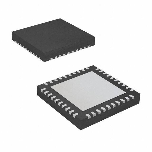
QFN40
MN SUFFIX
CASE 485AU
♦
© Semiconductor Components Industries, LLC, 2015
July, 2018 − Rev. 3
A
WL
YY
WW
G
= Assembly Location
= Wafer Lot
= Year
= Work Week
= Pb−Free Package
ORDERING INFORMATION
See detailed ordering and shipping information in the package
dimensions section on page 23 of this data sheet.
1
Publication Order Number:
NCN5110/D
�NCN5110
BLOCK DIAGRAM
VFILT
CAV
VBUS1
VDDA
VSSA
VDDD
Bus Coupler
VSSD
nDC2EN
Impedance
Control
nV20VEN
Receiver
TXD
RXD
CCP
VIN
TXO
Transmitter
VSW1
DC/DC
Converter 1
VDD1
VBUS2
FANIN
VDD1M
VSS1
NCN5110
Fan−In
Control
VDD2
V20V
RC
Osc
POR
XTAL1
XTAL2
DC/DC
Converter 2
20V LDO
VSS2
VSW2
VDD2MC
VDD2MV
OSC
TW
TSD
UVD
XCLKC
Diagnostics
XCLK
SAVEB
RESETB
Figure 1. Block Diagram NCN5110
31
32
33
34
35
36
37
38
1
30
2
29
3
28
4
27
NCN5110
5
6
26
25
20
19
18
17
VDDD
nDC2EN
TXD
RXD
nV20VEN
TEST4
TEST3
TEST2
TEST1
XCLKC
VIN
VSW1
VSS1
VDD1
VDD1M
VDD2MV
VDD2MC
VDD2
VSS2
VSW2
16
21
15
22
10
14
23
9
13
24
8
12
7
11
VSSA
VBUS2
TXO
CCP
CAV
VBUS1
CEQ1
CEQ2
VFILT
V20V
39
40
VDDA
TEST6
FANIN
RESETB
SAVEB
XTAL1
XTAL2
TEST5
XCLK
VSSD
PIN OUT
Figure 2. Pin Out NCN5110 (Top View)
www.onsemi.com
2
�NCN5110
PIN DESCRIPTION
Table 1. PIN LIST AND DESCRIPTION
Name
Pin
Description
VSSA
1
Analog Supply Voltage Ground
VBUS2
2
Ground for KNX Transmitter
TX0
3
KNX Transmitter Output
CCP
4
CAV
5
VBUS1
6
KNX power supply input
CEQ1
7
CEQ2
8
VFILT
9
V20V
10
VDD2MV
11
VDD2MC
VDD2
Type
Equivalent
Schematic
Supply
Supply
Analog Output
Type 1
AC coupling external capacitor connection
Analog I/O
Type 2
Capacitor connection to average bus DC voltage
Analog I/O
Type 3
Supply
Type 5
Capacitor connection 1 for defining equalization pulse
Analog I/O
Type 4
Capacitor connection 2 for defining equalization pulse
Analog I/O
Type 4
Filtered bus voltage
Supply
Type 5
20V supply output
Supply
Type 5
Voltage monitor of Voltage Regulator 2
Analog Input
Type 8
12
Current monitor input 1 of Voltage Regulator 2
Analog Input
Type 9
13
Current monitor input 2 of Voltage Regulator 2
Analog Input
Type 8
VSS2
14
Voltage Regulator 2 Ground
VSW2
15
Switch output of Voltage Regulator 2
VIN
16
Voltage Regulator 1 and 2 Power Supply Input
VSW1
17
Switch output of Voltage Regulator 1
VSS1
18
Voltage Regulator 1 Ground
VDD1
19
Current Input 2 and Voltage Monitor Input of Voltage Regulator 1
Analog Input
VDD1M
20
Current Monitor Input 1 of Voltage Monitor 1
Analog Input
Type 9
XCLKC
21
Clock Frequency Configure
Digital Input
Type 12
TEST1
22
Test pin. Leave unconnected.
Digital Output
Type 13
TEST2
23
Test pin. Connect to VSS.
Digital Input
Type 12
TEST3
24
Test pin. Connect to VSS.
Digital Input
Type 12
Supply
Analog Output
Type 6
Supply
Type 5
Analog Output
Type 6
Supply
Type 8
TEST4
25
Test pin. Connect to VSS.
Digital Input
Type 12
nV20VEN
26
20 V LDO Disable
Digital Input
Type 14
RXD
27
Receive Input
Digital Input
Type 14
TXD
28
Transmit Output
Digital Output
Type 13
nDC2EN
29
Voltage Regulator 2 Disable
Digital Input
Type 14
VDDD
30
Digital Supply Voltage Input
Supply
Type 7
VSSD
31
Digital Supply Voltage Ground
Supply
XCLK
32
Oscillator Clock Output
TEST5
33
Test pin. Connect to VSS.
XTAL2
34
Clock Generator Output (Quartz)
Digital Output
Type 13
Digital Input
Type 12
Analog Output
Type 10
XTAL1
35
Clock Generator Input (Quartz)
Analog Input
Type 10
SAVEB
36
Save Signal (open drain with pull−up)
Digital Output
Type 15
RESETB
37
Reset Signal (open drain with pull−up)
Digital Output
Type 15
FANIN
38
Fan−In Input
Analog Input
Type 11
TEST6
39
Test pin. Leave unconnected.
Analog Output
Type 16
VDDA
40
Analog Supply Voltage Input
Supply
Type 7
www.onsemi.com
3
�NCN5110
EQUIVALENT SCHEMATICS
Following figure gives the equivalent schematics of the user relevant inputs and outputs. The diagrams are simplified
representations of the circuits used.
CCP
60V
CAV
TXO
CEQx
7V
60V
60V
Type 1: TXO−pin
Type 2: CCP−pin
60V
Type 3: CAV−pin
Type 4: CEQ1− and
CEQ2−pin
VIN
VBUS1
VFILT
V20V
VDDD
VIN
VDDA
60V
VBUS1
VFILT
V20V
VDDD
VIN
VDDA
VSWx
60V
60V
60V
7V
60V
Type 5: VBUS1−, VFILT−, V20V and VIN−pin
7V
Type 7: VDDD− and VDDA−pin
Type 6: VSW1− and
VSW2−pin
VDD1
VDD2
7V
VDD1
VDD2
VDD2MV
7V
VDD1M
60V
7V
VDD2MC
60V
7V
Type 8: VDD1−, VDD2− and VDD2MV−pin
VDDD
7V
Type 9: VDD1M− and VDD2MC−pin
VAUX
VDDD
VDDD
XTAL2
FANIN
XTAL1
IN
7V
Type 10: XTAL1− and XTAL2−pin
VDDD
RDOWN
Type 12: TEST2−, TEST3−,
TEST4−, TEST5− and XCLKC−pin
Type 11: FANIN−pin
VDDA
VDDD
VDDD
RUP
OUT
IN
Type 13: TXD−, XCLK−
and TEST1−pin
TEST8
OUT
Type 14: nV20VEN−,
nDC2EN− and RXD−pin
Type 15: RESETB− and
SAVEB−pin
Figure 3. In− and Output Equivalent Diagrams
www.onsemi.com
4
Type 16: TEST6−pin
�NCN5110
ELECTRICAL SPECIFICATION
Table 2. ABSOLUTE MAXIMUM RATINGS (Notes 1 and 2)
Symbol
Parameter
Min
Max
Unit
−0.3
+45
V
250
mA
VTXO
KNX Transmitter Output Voltage
ITXO
KNX Transmitter Output Current (Note 3)
VCCP
Voltage on CCP−pin
−10.5
+14.5
V
VCAV
Voltage on CAV−pin
−0.3
+3.6
V
VBUS1
Voltage on VBUS1−pin
−0.3
+45
V
IBUS1
Current Consumption VBUS1−pin
0
120
mA
VFILT
Voltage on VFILT−pin
−0.3
+45
V
V20V
Voltage on V20V−pin
−0.3
+25
V
VDD2MV
Voltage on VDD2MV−pin
−0.3
+3.6
V
VDD2MC
Voltage on VDD2MC−pin
−0.3
+45
V
VDD2
Voltage on VDD2−pin
−0.3
+45
V
VSW
Voltage on VSW1− and VSW2−pin
−0.3
+45
V
VIN
Voltage on VIN−pin
−0.3
+45
V
Voltage on VDD1−pin
−0.3
+3.6
V
Voltage on VDD1M−pin
−0.3
+3.6
V
VDIG
Voltage on pins nV20VEN, nDC2EN, TXD, RXD, XCLK, SAVEB, RESETB,
XCLKC, and FANIN
−0.3
+3.6
V
VDD
Voltage on VDDD− and VDDA−pin
−0.3
+3.6
V
VXTAL
Voltage on XTAL1− and XTAL2−pin
−0.3
+3.6
V
Storage temperature
−55
+150
°C
Junction Temperature (Note 4)
−40
+155
°C
Human Body Model electronic discharge immunity (Note 5)
−2
+2
kV
VDD1
VDD1M
TST
TJ
VHBM
Stresses exceeding those listed in the Maximum Ratings table may damage the device. If any of these limits are exceeded, device functionality
should not be assumed, damage may occur and reliability may be affected.
1. Convention: currents flowing in the circuit are defined as positive.
2. VBUS2, VSS1, VSS2, VSSA and VSSD form the common ground. They are hard connected to the PCB ground layer.
3. Room temperature, 27 W shunt resistor for transmitter, 250 mA over temperature range.
4. Normal performance within the limitations is guaranteed up to the Thermal Warning level. Between Thermal Warning and Thermal Shutdown
temporary loss of function or degradation of performance (which ceases after the disturbance ceases) is possible.
5. According to JEDEC JESD22−A114.
www.onsemi.com
5
�NCN5110
RECOMMENDED OPERATING RANGES
Operating ranges define the limits for functional operation and parametric characteristics of the device. Note that the
functionality of the chip outside these operating ranges is not guaranteed. Operating outside the recommended operating ranges
for extended periods of time may affect device reliability.
Table 3. OPERATING RANGES
Symbol
VBUS1
Parameter
VBUS1 Voltage (Note 6)
VDD
Digital and Analog Supply Voltage (VDDD− and VDDA−pin)
VIN
Input Voltage DC−DC Converter 1 and 2
Min
Max
Unit
+20
+33
V
+3.13
+3.47
V
(Note 7)
+33
V
VCCP
Input Voltage at CCP−pin
−10.5
+14.5
V
VCAV
Input Voltage at CAV−pin
0
+3.3
V
VDD1
Input Voltage on VDD1−pin
+3.13
+3.47
V
Input Voltage on VDD1M−pin
+3.13
+3.57
V
VDD1M
Input Voltage on VDD2−pin
+1.2
+21
V
VDD2MC
VDD2
Input Voltage on VDD2MC−pin
+1.2
+21.1
V
VDD2MV
Input Voltage on VDD2MV−pin
+1.2
VDD
V
Input Voltage on pins nV20VEN, nDC2EN, RXD and XCLKC
0
VDD
V
Input Voltage on FANIN−pin
0
3.6
V
VDIG
VFANIN
fclk
Clock Frequency External Quartz
16
MHz
TA
Ambient Temperature
−40
+105
°C
TJ
Junction Temperature (Note 8)
−40
+125
°C
Functional operation above the stresses listed in the Recommended Operating Ranges is not implied. Extended exposure to stresses beyond
the Recommended Operating Ranges limits may affect device reliability.
6. Voltage indicates DC value. With equalization pulse bus voltage must be between 11 V and 45 V.
7. Minimum operating voltage on VIN−pin should be at least 1 V larger than the highest value of VDD1 and VDD2.
8. Higher junction temperature can result in reduced lifetime.
www.onsemi.com
6
�NCN5110
Table 4. DC PARAMETERS
(The DC parameters are given for a device operating within the Recommended Operating Conditions unless otherwise specified.
Convention: currents flowing in the circuit are defined as positive.)
Symbol
Pin(s)
Parameter
Remark/Test Conditions
Min
Typ
Max
Unit
33
V
POWER SUPPLY
VBUS1
IBUS1_Int
Excluding active and equalization
pulse
Bus DC voltage
VBUS1
Bus Current Consumption
20
VBUS = 30 V, IBUS = 10mA, DC2,
V20V disabled, no crystal or clock
1.25
1.70
VBUS = 20 V, IBUS = 40 mA
2.75
3.40
mA
VBUSH
Undervoltage release level
VBUS1 rising, see Figure 4
17.1
18.0
18.9
V
VBUSL
Undervoltage trigger level
VBUS1 falling, see Figure 4
15.9
16.8
17.7
V
VBUS_Hyst
Undervoltage hysteresis
0.6
VDDD
VDDD
Digital Power Supply
3.13
3.3
3.47
V
VDDA
VDDA
Analog Power Supply
3.13
3.3
3.47
V
2.8
3.3
3.6
V
FANIN floating, VFILT > VFILTH
0.40
0.50
FANIN = GND, VFILT > VFILTH
0.80
1.00
Resistor R6 = 10k, VFILT > VFILTH
1.51
1.95
Resistor R6 = 13.3k, VFILT > VFILTH
1.17
1.47
Resistor R6 = 20k, VFILT > VFILTH
0.78
0.98
Resistor R6 = 42.2k, VFILT > VFILTH
0.37
0.48
Resistor R6 = 93.1k, VFILT > VFILTH
0.17
0.23
30.0
VAUX
Auxiliary Supply
Internal supply, for info only
V
KNX BUS COUPLER
DIcoupler/Dt
Icoupler_lim,
startup
VBUS1
VBUS1
Bus Coupler Current Slope
Limitation
FANIN floating, VFILT > VFILTH
20.0
25.0
FANIN = GND, VFILT > VFILTH
40.0
50.0
60.0
Resistor R6 = 10k, VFILT > VFILTH
45.0
72.2
114.0
45.0
70.7
86.0
40.0
48.5
57.5
19.5
23.4
27.8
Resistor R6 = 93.1k, VFILT > VFILTH
9.4
11.3
13.1
FANIN floating, VFILT > VFILTH
10.8
11.4
12
FANIN = GND, VFILT > VFILTH
20.5
22.3
24
Resistor R6 = 10k, VFILT > VFILTH
39.6
43.9
47.0
Resistor R6 = 13.3k, VFILT > VFILTH
30.0
33.0
35.2
Resistor R6 = 20k, VFILT > VFILTH
20.2
22.1
23.6
Resistor R6 = 42.2k, VFILT > VFILTH
9.4
10.7
11.9
Resistor R6 = 93.1k, VFILT > VFILTH
4.2
Bus Coupler Startup Current
Resistor R6 = 13.3k, VFILT > VFILTH
Limitation
Resistor R6 = 20k, VFILT > VFILTH
Resistor R6 = 42.2k, VFILT > VFILTH
Icoupler_lim
Vcoupler_drop
VFILTH
VFILTL
VBUS1
VBUS1,
VFILT
VFILT
Bus Coupler Current
Limitation
Coupler Voltage Drop
(Vcoupler_drop = VBUS1 −
VFILT)
5.1
6.0
IBUS1 = 10 mA
1.72
2.32
IBUS1 = 20 mA
2.34
2.80
IBUS1 = 30 mA
2.94
3.40
IBUS1 = 40 mA
3.57
4.25
A/s
mA
mA
V
Undervoltage release level
VFILT rising, see Figure 5
10.1
10.6
11.2
V
Undervoltage trigger level
VFILT falling, see Figure 5
8.4
8.9
9.4
V
www.onsemi.com
7
�NCN5110
Table 4. DC PARAMETERS (continued)
(The DC parameters are given for a device operating within the Recommended Operating Conditions unless otherwise specified.
Convention: currents flowing in the circuit are defined as positive.)
Symbol
Pin(s)
Parameter
Remark/Test Conditions
Min
Typ
Max
Unit
33
V
3.3
3.47
V
FIXED DC−DC CONVERTER
VIN
VIN
VDD1
VDD1
Input Voltage
4.47
Output Voltage
3.13
VDD1_rip
Output Voltage Ripple
VIN = 25 V, IDD1 = 40 mA,
L1 = 220 mH
IDD1_lim
Overcurrent Threshold
R2 = 1 W
Power Efficiency
(DC Converter Only)
Vin = 25 V, IDD1 = 35 mA,
L1 = 220 mH (1.26 W ESR)
RDS(on)_p1
RDS(on) of power switch
See Figure 12
8
W
RDS(on)_n1
RDS(on) of flyback switch
See Figure 12
4
W
3.57
V
VDD2
+1
33
V
1.2
21
V
hVDD1
VDD1M
VDD1M
40
−100
mV
−200
90
Input voltage VDD1M−pin
mA
%
ADJUSTABLE DC−DC CONVERTER
VIN
VIN
VDD2
Input Voltage
Output Voltage
VIN ≥ VDD2
Undervoltage release level
VDD2 rising, see Figure 6
0.9 x
VDD2
V
Undervoltage trigger level
VDD2 falling, see Figure 6
0.8 x
VDD2
V
VDD2_rip
Output Voltage Ripple
VIN = 25 V, VDD2 = 3.3 V,
IDD2 = 40 mA, L2 = 220 mH
40
mV
IDD2_lim
Overcurrent Threshold
R3 = 1 W
Power Efficiency
(DC Converter Only)
Vin = 25 V, VDD2 = 3.3 V,
IDD2 = 35 mA, L2 = 220 mH (1.26 W
ESR)
RDS(on) of power switch
See Figure 12
RDS(on) of flyback switch
See Figure 12
VDD2H
VDD2
VDD2L
hVDD2
RDS(on)_p2
RDS(on)_n2
VDD2M
VDD2MC
Input voltage VDD2MC−pin
RVDD2M
VDD2MV
Input Resistance
VDD2MV−pin
Ileak,vsw2
−100
−250
90
mA
%
8
W
4
W
21.1
V
1
MW
Half−bridge leakage
20
mA
V20V REGULATOR
V20V
V20V Output Voltage
I20V_lim
V20V Output Current
Limitation
V20VH
V20V
V20VL
V20V_hyst
I20V < I20V_lim, VFILT ≥ 21 V
R6 > 250 kW
10 kW < R6 < 93.1 kW
18
20
22
V
4.34
5.68
8.00
mA
132.0/R6 273.4/R6 392.0/R6
A
R6 < 2 kW
9.52
12.37
16.00
mA
V20V Undervoltage release
level
V20V rising, see Figure 7
14.2
15.0
15.8
V
V20V Undervoltage trigger
level
V20V falling, see Figure 7
13.2
14.0
14.8
V
V20V Undervoltage
hysteresis
V20V_hyst = V20VH – V20VL
1.0
V
XTAL OSCILLATOR
VXTAL
XTAL1, XTAL2 Voltage on XTAL−pin
VDDD
V
40
mA
FAN−IN CONTROL
Ipu,fanin
FANIN
Pull−Up Current FANIN−pin
FANIN shorted to GND,
Pull−up connected to VAUX
www.onsemi.com
8
10
20
�NCN5110
Table 4. DC PARAMETERS (continued)
(The DC parameters are given for a device operating within the Recommended Operating Conditions unless otherwise specified.
Convention: currents flowing in the circuit are defined as positive.)
Symbol
Pin(s)
Parameter
Remark/Test Conditions
Min
Typ
Max
Unit
DIGITAL INPUTS
VIH
nV20VEN,
nDC2EN,
RXD, XCLKC
RDOWN
XCLKC
VIL
Logic Low Threshold
0
0.7
V
Logic High Threshold
2.65
VDDD
V
28
kW
Internal Pull−Down Resistor
5
10
Logic low output level
0
0.4
V
Logic high output level
VDDD −
0.45
VDDD
V
8
mA
DIGITAL OUTPUTS
VOL
VOH
TXD, XCLK
XCLK
IL
VOL
Rup
TXD
SAVEB,
RESETB
Load Current
Logic low level open drain
IOL = 4 mA
Internal Pull−up Resistor
4
mA
0.4
V
20
40
80
kW
TEMPERATURE MONITOR
TTW
Thermal Warning
Rising temperature
See Figure 8
105
115
125
°C
TTSD
Thermal shutdown
Rising temperature
See Figure 8
130
140
150
°C
THyst
Thermal Hysteresis
See Figure 8
5
11
15
°C
DT
Delta TTSD and TTW
See Figure 8
21.7
°C
Simulated Conform
JEDEC JESD−51, (2S2P)
30
K/W
Simulated Conform
JEDEC JESD−51, (1S0P)
60
K/W
0.95
K/W
PACKAGE THERMAL RESISTANCE VALUE
Thermal Resistance
Junction−to−Ambient
Rq,ja
Thermal Resistance
Junction−to−Exposed Pad
Rq,jp
Table 5. AC PARAMETERS
(The AC parameters are given for a device operating within the Recommended Operating Conditions unless otherwise specified.)
Pin(s)
Symbol
Parameter
Remark/Test Conditions
Min
Typ
Max
Unit
POWER SUPPLY
tBUS_FILTER
VBUS1
VBUS1 filter time
See Figure 4
2
ms
Rising slope at VSW1−pin
0.45
V/ns
Falling slope at VSW1−pin
0.6
V/ns
Rising slope at VSW2−pin
0.45
V/ns
Falling slope at VSW2−pin
0.6
V/ns
XTAL1, XTAL2 XTAL Oscillator Frequency
16
MHz
FIXED DC−DC CONVERTER
tVSW1_rise
tVSW1_fall
VSW1
ADJUSTABLE DC−DC CONVERTER
tVSW2_rise
tVSW2_fall
VSW2
XTAL OSCILLATOR
fXTAL
Product parametric performance is indicated in the Electrical Characteristics for the listed test conditions, unless otherwise noted. Product
performance may not be indicated by the Electrical Characteristics if operated under different conditions.
www.onsemi.com
9
�NCN5110
VBUS
VBUSH
VBUSL
t BUS_FILTER
t BUS_FILTER
Comments:
is an internal signal which ca be verified with the Internal State Service.
Figure 4. Bus Voltage Undervoltage Threshold
VFILT
VFILTH
VFILTL
t
Comments:
is an internal signal which ca be verified with the Internal State Service.
Figure 5. VFILT Undervoltage Threshold
VDD2
VDD2H
VDD2L
t
Comments:
is an internal signal which ca be verified with the Internal State Service.
Figure 6. VDD2 Undervoltage Thresholds
www.onsemi.com
10
t
�NCN5110
V20V
V20V_hyst
V20VH
V20VL
t
Comments:
is an internal signal which ca be verified with the Internal State Service.
THyst
Figure 7. V20V Undervoltage Threshold levels
T
TTW
THyst
TTSD
nT
t
SAVEB
Normal
Stand-By
Start-Up
Reset
Stand-By
Normal
RESETB
Comments:
− is an internal signal which can be verified with the System State Service
− No communication possible when RESETB is low!
− It’s assumed all voltage supplies are withing their operating condition.
Figure 8. Temperature Monitoring Levels
www.onsemi.com
11
Analog State
�NCN5110
TYPICAL APPLICATION SCHEMATICS
RESETb
SAVEb
R6
3.3
3.3
C5
VSSD
31
XCLK
32
TEST5
33
XTAL2
34
XTAL1
35
36
SAVEB
RESETB
37
38
FANIN
TEST6
RXD
nV20VEN
TEST4
TEST3
TEST2
TEST1
XCLKC
20
VDD1M
19
21
18
10
C7
B
39
22
11
C4
9
VDD2MV
C3
23
VDD1
V20V
8
17
VFILT
24
VSS1
D2
CEQ2
TxD
TXD
25
7
16
C2
6
VSW1
CEQ1
nDC2EN
26
NCN5110
C6
VDDD
27
5
15
VBUS1
4
VIN
CAV
28
14
C1
3
VSW2
CCP
29
13
A
2
VSS2
TXO
12
VBUS2
R1
3.3
30
VDD2
D1
GND
1
VDD2MC
VSSA
40
VDDA
VCC
3.3
C 10
L1
L2
R5
R2
R4
R3
V2
C 11
Figure 9. Typical Application Schematic, 20 mA Bus Current Limit and 1.0 mA/ms Bus Current Slopes
www.onsemi.com
12
RxD
�NCN5110
Table 6. EXTERNAL COMPONENTS LIST AND DESCRIPTION
Comp.
Function
Min
Typ
Max
Unit
Remarks
Notes
C1
AC coupling capacitor
42.3
47
51.7
nF
50 V, Ceramic
9
C2
Equalization capacitor
198
220
242
nF
50 V, Ceramic
9
C3
Capacitor to average bus DC voltage
80
100
120
nF
50 V, Ceramic
9
C4
Storage and filter capacitor VFILT
12.5
100
4000
mF
35 V
9, 15
C5
VDDA HF rejection capacitor
80
100
nF
6.3 V, Ceramic
C6
VDDD HF rejection capacitor
80
100
nF
6.3 V, Ceramic
C7
Load Capacitor V20V
1
mF
35 V, Ceramic, ESR < 2 W
C10
Load capacitor VDD1
8
10
mF
6.3 V, Ceramic, ESR < 0.1 W
C11
Load capacitor VDD2
8
10
mF
Ceramic, ESR < 0.1 W
10
R1
Shunt resistor for transmitting
24.3
27
29.7
W
1W
9
R2
DC1 sensing resistor
0.47
1
10
W
1/16 W
R3
DC2 sensing resistor
0.47
1
10
W
1/16 W
R4
Voltage divider to specify VDD2
W
1/16 W, see p15 for
calculating the exact value
R5
L1, L2
0
0
DC1/DC2 inductor
D1
Reverse polarity protection diode
D2
Voltage suppressor
R6
Fan-In Programming Resistor
1000
220
kW
12, 13, 15
mH
SS16
11
1SMA40CA
10
93.1
kW
1% precision
14
9. Component must be between minimum and maximum value to fulfill the KNX requirement.
10. Voltage of capacitor depends on VDD2 value defined by R4 and R5. See p16 for more details on defining VDD2 voltage value.
11. Reverse polarity diode is mandatory to fulfill the KNX requirement.
12. It’s allowed to short this pin to VFILT-pin
13. High capacitor value might affect the start up time
14. If no resistor connected or pulled up to 3.3 V the KNX device should be certified as a bus load of 10 mA. If shorted to ground the KNX device
should be certified as a bus load of 20 mA. If a resistor to ground is connected between 10 kW and 93.1 kW the device should be certified
as a bus load of 10 mA (42.2 k), 20 mA (20 k), 30 mA (13.3 k) or 40 mA (10 k).
15. Total charge of C4 and C7 may not be higher than 121 mC to fulfill the KNX requirement.
www.onsemi.com
13
�NCN5110
ANALOG FUNCTIONAL DESCRIPTION
The active pulse is produced by the transmitter and is
ideally rectangular. It has a duration of 35 ms and a depth
between 6 and 9 V (Vact). Each active pulse is followed by
an equalization pulse with a duration of 69 ms. The latter is
an abrupt jump of the bus voltage above the DC level
followed by an exponential decay down to the DC level. The
equalization pulse is characterized by its height Veq and the
voltage Vend reached at the end of the equalization pulse.
See the KNX Twisted Pair Standard (KNX TP1−256) for
more detailed KNX information.
Because NCN5110 follows the KNX standard only a brief
description of the KNX related blocks is given in this
datasheet. Detailed information on the KNX Bus can be
found on the KNX website (www.knx.org) and in the KNX
standards.
KNX Bus Interfacing
Each bit period is 104 ms. Logic 1 is simply the DC level
of the bus voltage which is between 20 V and 33 V. Logic 0
is encoded as a drop in the bus voltage with respect to the DC
level. Logic 0 is known as the active pulse.
Veq
V end
VBUS
Vact
DC Level
Active Pulse
t
Equalization Pulse
35 ms
69ms
104 ms
104 ms
1
0
Figure 10. KNX Bus Voltage versus Digital Value
KNX Bus Transmitter
the average bus voltage. The bus coupler also makes sure
that the current drawn from the bus changes very slowly. For
this a large filter capacitor is used on the VFILT−pin. Abrupt
load current steps are absorbed by the filter capacitor.
Long−term stability requires that the average bus coupler
input current is equal to the average (bus coupler) load
current. This is shown by the parameter DIcoupler/Dt, which
indicated the bus current slope limit. The bus coupler will
also limit the current to a maximum of Icoupler_lim. At
startup, this current limit is increased to Icoupler_lim,startup to
allow for fast charging of the VFILT bulk capacitance.
There are 4 conditions that determine the dimensioning of
the VFILT capacitor.
First, the capacitor value should be between 12.5 mF and
4000 mF to garantuee proper operation of the part.
The next requirement on the VFILT capacitor is
determined by the startup time of the system. According to
the KNX specification, the total startup time must be below
10s. This time is comprised of the time to charge the VFILT
capacitor to 12 V (where the DCDC convertor becomes
operatonal) and the startup time of the rest of the system
tstartup,system. This gives the following formula:
The purpose of the transmitter is to produce an active
pulse (see Figure 10) between 6 V and 9 V regardless of the
bus impedance (Note 1). In order to do this the transmitter
will sink as much current as necessary until the bus voltage
drops by the desired amount. The transmitter will produce
an active pulse whenever the TX pin is brought high. It is up
to the microcontroller to provide the bit−level coding and
provide the correct active pulse duration.
KNX Bus Receiver
The receiver detects the beginning and the end of the
active pulse. The detection threshold for the start of the
active pulse is −0.45 V (typ.) below the average bus voltage.
The detection threshold for the end of the active pulse is
−0.2 V (typ.) below the average bus voltage giving a
hysteresis of 0.25 V (typ.). The result of this detection is
available as a pulse on the RXD pin.
Bus Coupler
The role of the bus coupler is to extract the DC voltage
from the bus and provide a stable voltage supply for the
purpose of powering the NCN5110. This stable voltage
supplied by the bus coupler is called VFILT, and will follow
1. Maximum bus impedance is specified in the KNX Twisted Pair Standard
www.onsemi.com
14
�NCN5110
Ct
ǒ10s * tstartup,systemǓ
Although both DC−DC converters are capable of
delivering 100 mA, the maximum current capability will not
always be usable. One always needs to make sure that the
KNX bus power consumption stays within the KNX
specification. The maximum allowed current for the DC−DC
converters and V20V regulator can be estimated as next:
I coupler_lim,startup
VFILTH
The third limit on VFILT capacitor value is the required
capacitor value to filter out current steps DIstep of the system
without going into reset.
Cu
ǒ2 ǒV
DI step
2
Ǔ
BUS1 * V coupler_drop * V FILTL
I slope
V BUS
Ǔ
2
The last condition on the size of VFILT is the desired
warning time twarning between SAVEB and RESETB in
case the bus voltage drops away. This is determined by the
current consumption of the system Isystem.
Cu
I system
ǒtwarning ) tbusfilterǓ
The bus coupler is implemented as a linear voltage
regulator. For efficiency purpose, the voltage drop over the
bus coupler is kept minimal (see Table 4).
KNX Impedance Control
The impedance control circuit defines the impedance of
the bus device during the active and equalization pulses. The
impedance can be divided into a static and a dynamic
component, the latter being a function of time. The static
impedance defines the load for the active pulse current and
the equalization pulse current. The dynamic impedance is
produced by a block, called an equalization pulse generator,
that reduces the device current consumption (i.e. increases
the device impedance) as a function of time during the
equalization phase so as to return energy to the bus.
w1
(eq. 2)
This is the 20 V low drop linear voltage regulator used to
supply external devices. As it draws current from VFILT,
this current is seen without any power conversion directly at
the VBUS1 pin.
The V20V regulator is enabled by pulling the nV20VEN
pin low. When the nV20VEN pin is pulled high, the 20V
regulator is disabled. When the V20V regulator is not used,
no load capacitor needs to be connected (see C7 of Figure 9).
Connect V20V−pin with VFILT−pin in this case.
The 20 V regulator has a current limit that depends on the
FANIN resistor value. In Table 4, the typical value of the
current limit at startup is given as I20V_lim.
The device contains two DC−DC buck converters, both
supplied from VFILT.
DC1 provides a fixed voltage of 3.3 V. This voltage is used
as an internal low voltage supply (VDDA and VDDD) but can
also be used to power external devices (VDD1−pin). DC1 is
automatically enabled during the power−up procedure (see
Analog State Diagram, p19).
DC2 provides a programmable voltage by means of an
external resistor divider. It is not used as an internal voltage
supply making it not mandatory to use this DC−DC
converter (if not needed, tie the VDD2MV pin to VDD1).
DC2 will only be enabled when the nDC2EN pin is pulled
low. When nDC2EN is pulled to VDDD, the DC2 controller
is disabled.
The voltage divider can be calculated as follows:
1.2
ƫ
I DD2Ǔ
V20V Regulator
Fixed and Adjustable DC−DC Converter
V DD2 * 1.2
I DD1Ǔ ) ǒV DD2
IBUS will be limited by the KNX standard and should be
lower or equal to Icoupler (see Table 4). Minimum VBUS is
20 V (see KNX standard). VDD1 and VDD2 can be found back
in Table 4. IDD1, IDD2 and I20V must be chosen in a correct
way to be in line with the KNX specification (Note 2).
Although DC2 can operate up to 21 V, it will not be
possible to generate this 21 V under all operating conditions.
See application note AND9135 for defining the optimum
inductor and capacitor of the DC−DC converters. When
using low series resistance output capacitors on DC2, it is
advised to split the current sense resistor as shown in
Figure 12 to reduce ripple current for low load conditions.
ǒVBUS1 * Vcoupler_drop * VFILTLǓ
R4 + R5
ƪǒVDD1
ǒIBUS * I20VǓ
Xtal Oscillator
An analog oscillator cell generates an optional clock of
16 MHz.
XTAL2 34
XTAL1 35
OSC
32
21 VDD
XCLK
XCLKC
8 MHz @ XCLC = VSS
16 MHz @ XCLC = VDD
(eq. 1)
Figure 11. XTAL Oscillator
Both DC−DC converters make use of slope control to
improve EMC performance (see Table 5). To operate DC1
and DC2 correctly, the voltage on the VIN−pin should be
higher than the highest value of DC1 and DC2.
The XCLK−pin can be used to supply a clock signal to the
host controller.
2. The formula is for a typical KNX application. It‘s only given as guidance and does not guarantee compliance with the KNX standard.
www.onsemi.com
15
�NCN5110
values, the typical current limit can be approximated by the
formula Ibus = 0.0004 + 434/R6 A. Using different resistor
values is, however, not recommended.
Definitions for Start−Up and Normal Operation (as given
above) can be found in the KNX Specification.
After power−up, a 4 MHz (Note 3) clock signal will be
present on the XCLK−pin during Stand−By. When Normal
State is entered, a 8 or 16 MHz clock signal will be present
on the XCLK−pin. See also Figure 14. To output an 8 MHz
clock on the XCLK pin, the XCLKC pin must be pulled to
ground. When the XCLKC pin is pulled up to VDDD, the
XCLK pin will output a 16 MHz clock signal.
When Normal State is left and Stand−By State is
re−entered due to an issue different than an Xtal issue, the 8
or 16 MHz clock signal will still be present on the
XCLK−pin during the Stand−By State. If however
Stand−By is entered from Normal State due to an Xtal issue,
the 4 MHz clock signal will be present on the XCLK−pin.
See also Table 7.
RESETB− and SAVEB−pin
The RESETB signal can be used to keep the host
controller in a reset state. When RESETB is low this
indicates that the bus voltage is too low for normal operation
and that the fixed DC−DC converter has not started up. It
could also indicate a Thermal Shutdown (TSD). The
RESETB signal also indicates if communication between
host and NCN5110 is possible.
The SAVEB signal indicates correct operation. When
SAVEB goes low, this indicates a possible issue (loss of bus
power or too high temperature) which could trigger the host
controller to save critical data or go to a save state. SAVEB
goes low immediately when VFILT goes below 14 V (due
to sudden large current usage) or after 2 ms when VBUS
goes below 20 V. RESETB goes low when VFILT goes
below 12 V.
RESETB− and SAVEB−pin are open−drain pins with an
internal pull−up resistor to VDDD.
FANIN−pin
The FANIN−pin defines the maximum allowed bus
current and bus current slopes. If the FANIN−pin is kept
floating, pulled up to VDD, or pulled down with a resistance
higher than 250 kW, NCN5110 will limit the KNX bus
current slopes to 0.5 mA/ms at all times. NCN5110 will also
limit the KNX bus current to 30 mA during start−up. During
normal operation, NCN5110 is capable of taking 10.6 mA
(= Icoupler) from the KNX bus for supplying external loads
(DC1, DC2 and V20V).
If the FANIN−pin is pulled to ground with a resistance
smaller than 2 kW the operation is similar as above with the
exception that the KNX bus current slopes will be limited to
1 mA/ms at all times, the KNX bus current will be limited
to 60 mA during start−up and up to 20.5 mA (Icoupler) can be
taken from the KNX bus during normal operation. When the
FANIN−pin is pulled to ground with a resistance between
10 kW and 93.1 kW, the current slope and current limit are
defined by the values from Table 4. For different resistor
Voltage Supervisors
NCN5110 has different voltage supervisors monitoring
VBUS, VFILT, VDD2 and V20V. The general function of a
voltage supervisor is to detect when a voltage is above or
below a certain level. The levels for the different voltages
monitored can be found back in Table 4 (see also Figures 4,
5, 6 and 7).
Depending on the voltage supervisor outputs, the device
can enter different states (see Analog State Diagram, p19).
3. The 4 MHz clock signal is internally generated and will be less accurate as the crystal generated clock signal of 8 or 16 MHz.
www.onsemi.com
16
�NCN5110
VIN
From VFILT
P1
VSW1
Switch
Controller
L1
1W
VDD1 = 3.3 V
N1
10 mF
VSS1
VDD1M
COMP
VDD1
P2
VSW2
Switch
Controller
L2
0.47 W
0.47 W
N2
VDD2 = 1.2 V − 20 V
10 mF
VSS2
R4
VDD2MV
COMP
VDD2MC
VDD2
R5
NCN5110
Figure 12. Fixed (VDD1) and Adjustable (VDD2) DC−DC Converter
www.onsemi.com
17
�NCN5110
Table 7. STATUS OF SEVERAL BLOCKS DURING THE DIFFERENT (ANALOG) STATES
State
Osc
XCLK
VDD1
VDD2/V20V
COMMUNICATION
KNX
Reset
Off
Off
Off
Off
Inactive
Inactive
Start−Up
Off
Off
Start−up
Off
Inactive
Inactive
Stand−By (Note 16)
Off
4 MHz
On
Start−Up
Active
Active
Stand−By (Note 17)
On
(Note 19)
On
(Note 19)
On
On (Note 20)
Active
Active
Normal
On
On
(Note 18)
On
On
Active
Active
16. Only valid when entering Stand−By from Start−Up State.
17. Only valid when entering Stand−By from Normal State.
18. 8 MHz or 16 MHz depending on XCLKC.
19. 4 MHz signal if Stand−By state was entered due to oscillator issue. Otherwise 8 MHz or 16 MHz clock signal.
20. Only operational if Stand−By state was not entered due to VDD2 or V20V issue.
Temperature Monitor
protect the device). The device will stay in the Reset State
as long as the temperature stays above TTSD.
If the temperature drops below TTSD, Start−Up State will
be entered (see also Figure 13). At the moment VDD1 is
back up and the OTP memory is read, Stand−By State will
be entered and RESETB will go high. Once the temperature
has dropped below TTW and all voltages are high enough,
Normal State will be entered. SAVEB will go high and KNX
communication is again possible.
Figure 8 gives a better view on the temperature monitor.
The device produces an over−temperature warning (TW)
and a thermal shutdown warning (TSD). Whenever the
junction temperature rises above the Thermal Warning level
(TTW), the SAVEB−pin will go low to signal the issue to the
host controller. When the junction temperature is above TW,
the host controller should undertake actions to reduce the
junction temperature and/or store critical data.
When the junction temperature reaches Thermal
Shutdown (TTSD), the device will go to the Reset State and
the analog and digital power supply will be stopped (to
www.onsemi.com
18
�NCN5110
Analog State Diagram
(OTP memory is not accessible by the user). When done, the
Stand−By State is entered and the RESETB−pin is made
high. When VFILT is above VFILTH DC2 and V20V will be
started. When the VBUS−, VFILT−, VDD2− and V20V−
monitors are ok, the Normal State will be entered and
SAVEB−pin will go high.
Figure 15 gives a detailed view on the shut−down
behavior. If the KNX bus voltage drops below VBUSL for
more than tbus_filter, the Standy−By State is entered. SAVEB
will go low to signal this. When VFILT drops below VFILTL,
DC2 and the V20V regulator will be switched off. When
VFILT drops below 6.5 V (typ), DC1 will be switched off
and VDD1 drops below 2.8 V (typ.) the device goes to Reset
State (RESETB low).
The analog state diagram of NCN5110 is given in
Figure 13. The status of the DC−DC converters, V20V
regulator and KNX communication during the different
(analog) states is given in Table 7.
Figure 14 gives a detailed view on the start−up behavior
of NCN5110. After applying the bus voltage, the filter
capacitor starts to charge. During this Reset State, the
current drawn from the bus is limited to Icoupler (for details
see the KNX Standards). Once the voltage on the filter
capacitor reaches 10 V (typ.), the fixed DC−DC converter
(powering VDDA) will be enabled and the device enters the
Start−Up State. When VDD1 gets above 2.8 V (typ.), the
OTP memory is read out to trim some analog parameters
Reset
RESETB = ‘0’
SAVEB = ‘0’
V FILT > 12V
and
Temp < TSD
Enable DC1
Disable DC1
V FILT < 6.5V
Start−Up
RESETB = ‘0’
SAVEB = ‘0’
Disable DC1, DC2 and V20V
V DDA OK
and
OTP read done
Disable DC2 and V20V
Enable DC2 and V20V
V FILT > V FILTH
V FILT < 6.5V
V FILT < V FILTL
Stand−By
= ‘1’
or
V DDA nOK
RESETB = ‘1’
SAVEB = ‘0’
Disable DC1
= ‘1’ or = ‘0’ or
= ‘0’ or = ‘0’ or
= ‘0’ or = ‘0’
= ‘0’ and = ‘1’ and
= ‘1’ and = ‘1’ and
= ‘1’ and = ‘1’
= ‘1’
or
V DDA nOK
Normal
RESETB = ‘1’
SAVEB = ‘1’
Remarks:
− , , , , and are internal status bits
− is an internal signal indicating a Thermal Shutdown. This internal signal cannot be read out.
− Although Reset State could be entered from Normal State on a TSD, Stand−By State will be entered first due to a TW.
Figure 13. Analog State Diagram
www.onsemi.com
19
�NCN5110
VBUS
VFILT
V BUSH
VFILTH
12V
IBUS
Icoupler_lim,startup
VDD1
2.8V
VXTAL
Xtal Oscillator
±2ms
±2ms
VDD2
0.9 x V DD2
V20V
V 20VH
RESETB
SAVEB
XCLK
Reset
Start−Up
Remarks:
VDD1 directly connected to VDDA.
Figure 14. Start−Up Behavior
www.onsemi.com
20
Stand−By
Normal
t
�NCN5110
VBUS
VFILT
VBUSH
VBUSL
VFILTL
6.5V
IBUS
VDD1
2.8V
VXTAL
Xtal Oscillator
tbus_filter
tbus_filter
VDD2
0.9 x VDD2
V20V
RESETB
SAVEB
XCLK
t
Remarks:
VDD1 directly connected to VDDA.
Normal
Stand-By
Normal
Figure 15. Shut−Down Behavior
www.onsemi.com
21
Stand-By
Reset
�NCN5110
Communication Interface
level coding/decoding has to be done by the host controller.
Keep in mind that the signals on the RXD− and TXD−pin are
inverted. Figure 9 gives an application example.
The NCN5110 communication pins (TxD and RxD) are
connected immediately to the KNX transmitter/receiver. Bit
V
V eq
end
VBUS
V act
DC Level
TXD/RXD
Active Pulse
Equalization Pulse
35 ms
69 ms
t
3.3V
t
Figure 16. Bus Communication and the Corresponding Voltage Levels on RxD and TxD
www.onsemi.com
22
�NCN5110
PACKAGE THERMAL CHARACTERISTICS
The NCN5110 is available in a QFN40 package. For cooling optimizations, the QFN40 has an exposed thermal pad which
has to be soldered to the PCB ground plane. The ground plane needs thermal vias to conduct the heat to the bottom layer.
Figure 17 gives an example of good heat transfer. The exposed thermal pad is soldered directly on the top ground layer (left
picture of Figure 17). It‘s advised to make the top ground layer as large as possible (see arrows Figure 17). To improve the heat
transfer even more, the exposed thermal pad is connected to a bottom ground layer by using thermal vias (see right picture of
Figure 17). It‘s advised to make this bottom ground layer as large as possible and with as less as possible interruptions.
For precise thermal cooling calculations the major thermal resistances of the device are given (Table 4). The thermal media
to which the power of the devices has to be given are:
− Static environmental air (via the case)
− PCB board copper area (via the exposed pad)
The major thermal resistances of the device are the Rth from the junction to the ambient (Rthja) and the overall Rth from
the junction to exposed pad (Rthjp). In Table 4 one can find the values for the Rthja and Rthjp, simulated according to JESD−51.
The Rthja for 2S2P is simulated conform JEDEC JESD−51 as follows:
− A 4−layer printed circuit board with inner power planes and outer (top and bottom) signal layers is used
− Board thickness is 1.46 mm (FR4 PCB material)
− The 2 signal layers: 70 mm thick copper with an area of 5500 mm2 copper and 20% conductivity
− The 2 power internal planes: 36 mm thick copper with an area of 5500 mm2 copper and 90% conductivity
The Rthja for 1S0P is simulated conform to JEDEC JESD−51 as follows:
− A 1−layer printed circuit board with only 1 layer
− Board thickness is 1.46 mm (FR4 PCB material)
− The layer has a thickness of 70 mm copper with an area of 5500 mm2 copper and 20% conductivity
Figure 17. PCB Ground Plane Layout Condition
(left picture displays the top ground layer, right picture displays the bottom ground layer)
ORDERING INFORMATION
Temperature Range
Package
Shipping†
NCN5110MNG
−40°C to 105°C
QFN−40
(Pb−Free)
50 Units / Tube
100 Tubes / Box
NCN5110MNTWG
−40°C to 105°C
QFN−40
(Pb−Free)
3,000 / Tape & Reel
Device Number
†For information on tape and reel specifications, including part orientation and tape sizes, please refer to our Tape and Reel Packaging
Specification Brochure, BRD8011/D.
KNX and the KNX Logos are trademarks of KNX Association.
www.onsemi.com
23
�MECHANICAL CASE OUTLINE
PACKAGE DIMENSIONS
QFN40 6x6, 0.5P
CASE 485AU−01
ISSUE O
1 40
SCALE 2:1
PIN ONE
LOCATION
ÉÉ
ÉÉ
A B
D
L1
DETAIL A
E
OPTIONAL
CONSTRUCTIONS
ÉÉÉ
ÉÉÉ
EXPOSED Cu
TOP VIEW
OPTIONAL
CONSTRUCTIONS
A
0.08 C
A1
NOTE 4
0.10 C A B
D2
11
SEATING
PLANE
C
SIDE VIEW
DETAIL A
MOLD CMPD
DETAIL B
(A3)
DETAIL B
0.10 C
L
L
0.15 C
0.15 C
DATE 01 JUL 2008
NOTES:
1. DIMENSIONING AND TOLERANCING PER
ASME Y14.5M, 1994.
2. CONTROLLING DIMENSIONS: MILLIMETERS.
3. DIMENSION b APPLIES TO PLATED
TERMINAL AND IS MEASURED BETWEEN
0.15 AND 0.30mm FROM TERMINAL TIP.
4. COPLANARITY APPLIES TO THE EXPOSED
PAD AS WELL AS THE TERMINALS.
DIM
A
A1
A3
b
D
D2
E
E2
e
K
L
L1
MILLIMETERS
MIN
MAX
0.80
1.00
0.00
0.05
0.20 REF
0.18
0.30
6.00 BSC
3.10
3.30
6.00 BSC
3.10
3.30
0.50 BSC
0.20 MIN
0.30
0.50
−−−
0.15
GENERIC
MARKING DIAGRAM*
K
20
10
21
1
30
XXXXXXXX
AWLYYWWG
E2
0.10 C A B
L
31
40
e
40X
BOTTOM VIEW
b
0.10 C A B
0.05 C
SOLDERING FOOTPRINT*
6.30
*This information is generic. Please refer to
device data sheet for actual part marking.
Pb−Free indicator, “G” or microdot “ G”,
may or may not be present.
40X
0.63
3.32
XXX = Specific Device Code
A
= Assembly Location
WL = Wafer Lot
YY = Year
WW = Work Week
G = Pb−Free Package
1
3.32
6.30
PACKAGE
OUTLINE
40X
0.28
0.50 PITCH
DIMENSIONS: MILLIMETERS
*For additional information on our Pb−Free strategy and soldering
details, please download the ON Semiconductor Soldering and
Mounting Techniques Reference Manual, SOLDERRM/D.
DOCUMENT NUMBER:
DESCRIPTION:
98AON31154E
QFN40, 6x6, 0.5P
Electronic versions are uncontrolled except when accessed directly from the Document Repository.
Printed versions are uncontrolled except when stamped “CONTROLLED COPY” in red.
PAGE 1 OF 1
ON Semiconductor and
are trademarks of Semiconductor Components Industries, LLC dba ON Semiconductor or its subsidiaries in the United States and/or other countries.
ON Semiconductor reserves the right to make changes without further notice to any products herein. ON Semiconductor makes no warranty, representation or guarantee regarding
the suitability of its products for any particular purpose, nor does ON Semiconductor assume any liability arising out of the application or use of any product or circuit, and specifically
disclaims any and all liability, including without limitation special, consequential or incidental damages. ON Semiconductor does not convey any license under its patent rights nor the
rights of others.
© Semiconductor Components Industries, LLC, 2019
www.onsemi.com
�onsemi,
, and other names, marks, and brands are registered and/or common law trademarks of Semiconductor Components Industries, LLC dba “onsemi” or its affiliates
and/or subsidiaries in the United States and/or other countries. onsemi owns the rights to a number of patents, trademarks, copyrights, trade secrets, and other intellectual property.
A listing of onsemi’s product/patent coverage may be accessed at www.onsemi.com/site/pdf/Patent−Marking.pdf. onsemi reserves the right to make changes at any time to any
products or information herein, without notice. The information herein is provided “as−is” and onsemi makes no warranty, representation or guarantee regarding the accuracy of the
information, product features, availability, functionality, or suitability of its products for any particular purpose, nor does onsemi assume any liability arising out of the application or use
of any product or circuit, and specifically disclaims any and all liability, including without limitation special, consequential or incidental damages. Buyer is responsible for its products
and applications using onsemi products, including compliance with all laws, regulations and safety requirements or standards, regardless of any support or applications information
provided by onsemi. “Typical” parameters which may be provided in onsemi data sheets and/or specifications can and do vary in different applications and actual performance may
vary over time. All operating parameters, including “Typicals” must be validated for each customer application by customer’s technical experts. onsemi does not convey any license
under any of its intellectual property rights nor the rights of others. onsemi products are not designed, intended, or authorized for use as a critical component in life support systems
or any FDA Class 3 medical devices or medical devices with a same or similar classification in a foreign jurisdiction or any devices intended for implantation in the human body. Should
Buyer purchase or use onsemi products for any such unintended or unauthorized application, Buyer shall indemnify and hold onsemi and its officers, employees, subsidiaries, affiliates,
and distributors harmless against all claims, costs, damages, and expenses, and reasonable attorney fees arising out of, directly or indirectly, any claim of personal injury or death
associated with such unintended or unauthorized use, even if such claim alleges that onsemi was negligent regarding the design or manufacture of the part. onsemi is an Equal
Opportunity/Affirmative Action Employer. This literature is subject to all applicable copyright laws and is not for resale in any manner.
PUBLICATION ORDERING INFORMATION
LITERATURE FULFILLMENT:
Email Requests to: orderlit@onsemi.com
onsemi Website: www.onsemi.com
◊
TECHNICAL SUPPORT
North American Technical Support:
Voice Mail: 1 800−282−9855 Toll Free USA/Canada
Phone: 011 421 33 790 2910
Europe, Middle East and Africa Technical Support:
Phone: 00421 33 790 2910
For additional information, please contact your local Sales Representative
�