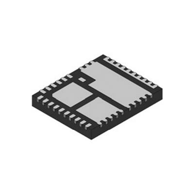
NCP303151
Integrated Driver and
MOSFET with Integrated
Current Monitor
Description
The NCP303151 integrates a MOSFET driver, high−side MOSFET
and low−side MOSFET into a single package.
The driver and MOSFETs have been optimized for high−current
DC−DC buck power conversion applications. The NCP303151
integrated solution greatly reduces package parasitics and board space
compared to a discrete component solution.
www.onsemi.com
Features
• Capable of Average Currents up to 50 A
• 30 V / 30 V Breakdown Voltage MOSFETs for Higher Long Term
•
•
•
•
•
•
•
•
•
Reliability
High−Performance, Universal Footprint, Copper−Clip 5 mm x 6 mm
PQFN Package
Capable of Switching at Frequencies up to 1 MHz
Compatible with 3.3 V or 5 V PWM Input
Responds Properly to 3−level PWM Inputs
Precise Current Monitoring
Option for Zero Cross Detection with 3−level PWM
Internal Bootstrap Diode
Catastrophic Fault Detection
♦ Thermal Flag (OTP) for Over−Temperature Condition
♦ Over−Current Protection FAULT (OCP)
♦ Under−Voltage Lockout (UVLO) on VCC and PVCC
Supports Intel® Power State 4
Applications
• Desktop & Notebook Microprocessors
• Graphic Cards
• Routers and Switches
PQFN39
MN SUFFIX
CASE 483BF
MARKING DIAGRAM
NCP
303151
AZZYYWW
NCP303151
A
ZZ
YY
WW
= Specific Device Code
= Assembly Location
= Wafer Lot
= Year
= Work Week
ORDERING INFORMATION
Device
Package
Shipping†
NCP303151MNTWG
5x6 PQFN
3000 / Tape &
Reel
†For information on tape and reel specifications,
including part orientation and tape sizes, please
refer to our Tape and Reel Packaging Specification
Brochure, BRD8011/D.
© Semiconductor Components Industries, LLC, 2018
August, 2018 − Rev. 1
1
Publication Order Number:
NCP303151/D
�NCP303151
DIAGRAMS
RVCC
V 5V
C PVCC
CVCC
PVCC
PWM
PWM from
controller
DRVON from
controller
VCC
RBOOT
VIN
BOOT
PHASE
FAULT
IOUT
SW
VOUT
L OUT
ZCD_EN
Current
sense
RefIN
Voltage
IIN
C BOOT
DISB#
Fault
ZCD_EN
V IN
C VIN
COUT
IMON
REFIN
AGND
PGND
Figure 1. Application Diagram
PVCC
3.3 V
BOOT
flag on FAULT
THERMAL
WARNING
FAULT
FAULT
LATCH
EN_PWM
IMON
VIN
IMON
FAULT LOGIC
REFIN
PHASE
1 V / 2.4 V
EN_POR
LEVEL
SHIFT
STARTUP
(POR)
EN/UVLO
EN_PWM
EN_POR
PWM CONTROL
LOGIC
VCC
EN_IC
REN_DOWN
EN_POR
DISB#
HDRV
SW
VCC
LDRV
RPWM_UP
PWM INPUT
STAGE
PWM
VCC
GL
RPWM_DOWN
EN_POR
ZCD_EN
ZCD
CONTROL
AGND
Figure 2. Block Diagram
www.onsemi.com
2
PGND
�NCP303151
PINOUT DIAGRAM
6.0 mm
N/C
1
AGND
2
VCC
3
PVCC
4
PGND
5
GL
6
REFIN
IMON
ZCD_EN
FAULT
DISB#
PWM
BOOT
PHASE
N/C
VIN
5.0 mm
39
38
37
36
35
34
33
32
31
30
40
GL
29
VIN
28
VIN
27
VIN
26
VIN
25
VIN
24
PGND
23
PGND
22
PGND
21
PGND
20
PGND
13
14
15
16
SW
17
18
19
SW
12
SW
11
SW
10
SW
PGND
9
SW
8
SW
PGND
SW
7
SW
PGND
SW
41
Figure 3. Top View
Table 1. PIN LIST AND DESCRIPTIONS
Pin No.
Symbol
1
NC
Description
2
AGND
3
VCC
4
PVCC
Power Supply input for LS Gate Driver and Boot Diode.
5, 40
PGND
Reserved for PVCC de−coupling capacitor return.
No connect.
Analog Ground for the analog portions of the IC and for substrate.
Power Supply input for all analog control functions
6, 41
GL
7−9, 20−24
PGND
Low−Side Gate Monitor.
10−19
SW
Switching node junction between high−and low−side MOSFETs
25−30
VIN
Input Voltage to Power Stage.
31
NC
No connect.
32
PHASE
Return Connection for BOOT capacitor.
33
BOOT
Supply for high−side MOSFET gate driver. A capacitor from BOOT to PHASE supplies the charge to turn
on the n−channel high side MOSFET. During the freewheeling interval (LS MOSFET on) the high side
capacitor is recharged by an internal diode.
34
PWM
PWM input to gate driver IC.
35
DISB#
Output disable pin. When this pin is pulled to a logic high level, the driver is enabled. There is an internal
pull−down resistor on this pin.
36
FAULT
FAULT Reporting Pin
37
ZCD_EN
38
IMON
Current Monitor Output (output is referenced to REFIN) − 5 mA/A
39
REFIN
Referenced voltage used for IMON feature. DC input voltage supplied by external source (not generated
on SPS driver IC)
Power ground connection for Power Stage high current path.
Zero Current Detection Function Enable
www.onsemi.com
3
�NCP303151
Table 2. ABSOLUTE MAXIMUM RATINGS (Electrical Information − all signals referenced to PGND unless noted otherwise)
Min
Max
Unit
VCC, PVCC
−0.3
6
V
VIN
−0.3
25
V
BOOT (DC)
−0.3
32
V
BOOT to PHASE (DC)
−0.3
7
V
VSW, PHASE (DC)
−0.3
25
V
−5
25
V
−0.3
VVCC + 0.3
V
Pin Name / Parameter
VSW, PHASE (< 5 ns)
All Other Pins
ESD
Human Body Model, JESD22−A114
2000
V
Charged Device Model, JESD22−C101
1000
V
Stresses exceeding those listed in the Maximum Ratings table may damage the device. If any of these limits are exceeded, device functionality
should not be assumed, damage may occur and reliability may be affected.
Table 3. THERMAL INFORMATION
Rating
Symbol
Value
Unit
qJA
12.4
°C/W
qJ−PCB
1.8
°C/W
Operating Junction Temperature Range (Note 1)
TJ
−40 to +150
°C
Operating Ambient Temperature Range
TA
−40 to +125
°C
Maximum Storage Temperature Range
TSTG
−55 to +150
°C
Moisture Sensitivity Level
MSL
1
Thermal Resistance (under On Semi SPS Thermal Board)
1. The maximum package power dissipation must be observed.
2. JESD 51−5 (1S2P Direct−Attach Method) with 0 LFM
3. JESD 51−7 (1S2P Direct−Attach Method) with 0 LFM
Table 4. RECOMMENDED OPERATING CONDITIONS
Parameter
Supply Voltage Range
Conversion Voltage
Continuous Output Current
Min
Typ
Max
Unit
VCC, PVCC
Pin Name
Conditions
4.5
5.0
5.5
V
VIN
4.5
12
16
V
FSW = 1 MHz, VIN = 12 V, VOUT = 1.0 V, TA = 25°C
45
A
FSW = 300 kHz, VIN = 12 V, VOUT = 1.0 V, TA = 25°C
50
A
FSW = 500 kHz, VIN = 12 V, VOUT = 1.0 V,
Duration = 10 ms, Period = 1 s, TA = 25°C
80
A
125
°C
Peak Output Current
Junction Temperature
−40
Functional operation above the stresses listed in the Recommended Operating Ranges is not implied. Extended exposure to stresses beyond
the Recommended Operating Ranges limits may affect device reliability.
Table 5. ELECTRICAL CHARACTERISTICS
(VVCC = 5.0 V, VVIN = 12 V, VDISB# = 2.0 V, CVCC = 0.1 mF unless specified otherwise) Min/Max values are valid for the temperature range
−40°C ≤ TJ ≤ 125°C unless noted otherwise, and are guaranteed by test, design or statistical correlation.
Parameter
Symbol
Conditions
Min
Typ
Max
Unit
VCC SUPPLY CURRENT
No switching
DISB# = 5 V, PWM = 0 V
−
8
−
mA
Disabled
DISB# = 0 V, SW = 0 V
−
120
−
mA
3.8
4.1
4.2
V
−
0.17
−
V
125
ms
UVLO Threshold
VUVLO
UVLO Hysteresis
UVLO_Hyst
POR Delay to Enable IC
TD_POR
VCC rising
VCC UVLO rising to internal PWM enable
www.onsemi.com
4
�NCP303151
Table 5. ELECTRICAL CHARACTERISTICS
(VVCC = 5.0 V, VVIN = 12 V, VDISB# = 2.0 V, CVCC = 0.1 mF unless specified otherwise) Min/Max values are valid for the temperature range
−40°C ≤ TJ ≤ 125°C unless noted otherwise, and are guaranteed by test, design or statistical correlation.
Parameter
Symbol
Conditions
Min
Typ
Max
Unit
DISB# INPUT
−
130
−
kW
High−Level Input Voltage
VUPPER
2.7
−
−
V
Low−Level Input Voltage
VLOWER
−
−
0.65
V
Pull−Down Resistance
Enable Propagation Delay
PWM=GND, Delay Between EN from
LOW to HIGH to GL from LOW to HIGH
– Slow EN Setting
16
26
32
ms
Disable Propagation Delay
PWM=GND, Delay Between EN from
HIGH to LOW to GL from HIGH to LOW
– Fast EN setting
−
43
109
ns
VPWM_HI
2.35
2.45
2.55
V
Mid−State Voltage Upper Threshold
VTRI_HI
2.05
2.2
2.3
V
Mid−State Voltage Lower Threshold
VTRI_LO
0.9
1.0
1.1
V
Input Low Voltage
VPWM_LO
0.65
0.75
0.85
V
Pull−Up Impedance
RUP_PWM
−
21
−
kW
Pull−Down Impedance
RDOWN_PWM
−
10
−
kW
3−State Open Voltage
VPWM_HIZ
1.4
1.65
1.85
V
Non−overlap Delay, Leading Edge
TDEADON
GL 1.2 V. PWM Transition 0→1
7
ns
Non−overlap Delay, Trailing Edge
TDEADOFF
SW =0.5 V, PWM Transition 1→0
6
ns
PWM Propagation Delay, Rising
TPD_PHGLL
PWM Going HIGH to GL Going LOW,
VIH_PWM to 90% GL
−
17
20
ns
PWM Propagation Delay, Falling
TPD_PLGHL
PWM Going LOW to GH Going LOW,
VIL_PWM to 90% GH
−
26
30
ns
Exiting PWM Mid−state Propagation
Delay, Mid−to−Low
TPWM_EXIT_L
PWM (from Tri−State) going LOW to
GL going HIGH, VIL_PWM to 10% GL
−
20
30
ns
Exiting PWM Mid−state Propagation
Delay, Mid−to−High
TPWM_EXIT_H
PWM (from Tri−State) going HIGH to
SW going HIGH, VIH_PWM to 10% SW
−
27
30
ns
PWM High to 3−State hold Off Time
TD_HOLDOFF1
PWM Going High to HS Going Off
20
43
50
ns
PWM Low to 3−State hold Off Time
TD_HOLDOFF2
PWM Going Low to LS Going Off
20
36
50
ns
HS minimal turn on time
TON_MIN_HS
SW gate rising 10% to falling 10%
37
ns
LS minimal turn on time
TON_MIN_LS
LS gate rising 10% to falling 10%
33
ns
HS minimal turn off time
TOFF_MIN_HS
SW gate falling 10% to rising 10%
31
ns
LS minimal turn off time
TOFF_MIN_LS
LS gate falling 10% to rising 10%
51
ns
PWM INPUT (TA=25°C, VCC / PVCC=5 V, fSW=1 MHz, IOUT=10 A)
Input High Voltage
FAULT FLAG OUTPUT VOLTAGE/CURRENT
FAULT Report Output Voltage
VFAULT
3
−
−
V
Fault Report Delay time
TDFAULT
−
100
−
ns
IMON
HS off to LS On Blanking Stop Time
TBLANK_HSOFF IMON Blanking Time for PWM transition 1³0
−
90
−
ns
HS on to LS Off Blanking Stop Time
TBLANK_HSON IMON Blanking Time for PWM transition 0³1
−
70
−
ns
−
5
−
MHz
IMON Amplifier Gain BW
BWIMON
L=150 nH, VIN=12 V, VOUT=1.0 V,
fSW=800 kHz
www.onsemi.com
5
�NCP303151
Table 5. ELECTRICAL CHARACTERISTICS
(VVCC = 5.0 V, VVIN = 12 V, VDISB# = 2.0 V, CVCC = 0.1 mF unless specified otherwise) Min/Max values are valid for the temperature range
−40°C ≤ TJ ≤ 125°C unless noted otherwise, and are guaranteed by test, design or statistical correlation.
Parameter
Symbol
Conditions
Min
Typ
Max
Unit
−
60
75
ns
2.3
V
IMON
TDELAY
IMON Propagation Delay Time
L=150 nH, VIN=12 V, VOUT=1.0 V,
fSW=800 kHz, IMON Peak to IL Peak
IMON OPERATING RANGE ( TA = TJ = −405C to 1255C, VCC = 4.5 V to 5.5 V, VIN = 4.5 − 20 V)
VIMON
Dynamic range at IMON pin
0.6
IMON ACCURACY (TA = 255C to 1255C, VCC/PVCC = 5 V, VIN = 12 V) (Note 4)
IMON_SLOPE
VIMON_10A
VIMON_20A
VIMON_30A
IMON_SLOPE
RIMON=1 kW
resistor placed
from IMON to
REFIN.
Current Monitor
Voltage
(VIMON−REFIN)
VIMON_40A
IOUT=−10 A to 30 A
4.75
5.00
5.25
mA/A
IOUT=10 A, Voltage is Referenced to
REFIN Pin
46.5
50
53.5
mV
IOUT = 20 A, Voltage is Referenced to
REFIN Pin
95
100
105
mV
IOUT = 30 A, Voltage is Referenced to
REFIN Pin
142.5
150
157.5
mV
IOUT = 40 A, Voltage is Referenced to
REFIN Pin
190
200
210
mV
−
350
−
mV
BOOTSTRAP DIODE
Forward Voltage
VF
Breakdown Voltage
VR
Forward Bias Current = 10 mA
30
V
LOW−SIDE DRIVER
Source Current=100 mA
−
0.64
−
W
Sink Current=100 mA
−
0.29
−
W
Over−Temperature Warning Accuracy
Driver IC Temperature
136
140
143
°C
OTW Hysteresis
Driver IC Temperature
15
°C
tD_ILimit−COMP Input Signal = 380 mV,
dv/dt = 0.2 mV/nsec.
60
ns
33
ns
Output Impedance, Sourcing
Output Impedance, Sinking
RSOURCE_GL
RSINK_GH
OVER−TEMPERATURE WARNING FAULT
HS CYCLE−BY−CYCLE POSITIVE I−LIMIT
I−limit comparator input−output propagation delay.
I−limit Blanking Time
Over−Current Limit
OCP Hysteresis
tBLANK_ILimit
De−glitch filter (blanking) time for I−limit
comparator trip
ILIM
74
ILIM_HYS
80
86
A
8
A
−50
A
NEGATIVE OVER−CURRENT (NOCP) FAULT
NOCP Trip LOW Level
INOCP_LOW
ZCD_EN INPUT
RUP_PWM
−
21
−
kW
Pull−Down Impedance
RDOWN_PWM
−
10
−
kW
3−State Open Voltage
VPWM_HIZ
1.4
1.65
1.85
V
Pull−Up Impedance
ZCD_EN input Voltage High
VZCD_HI
2.25
2.4
2.55
V
ZCD_EN input Voltage Mid−state
VZCD_MID
1.4
−
2.0
V
ZCD_EN input Voltage Low
VZCD_LO
0.75
0.8
0.85
V
Product parametric performance is indicated in the Electrical Characteristics for the listed test conditions, unless otherwise noted. Product
performance may not be indicated by the Electrical Characteristics if operated under different conditions.
4. Imon performance is guaranteed by independent ATE testing of High−side and Low−side slope and offset
www.onsemi.com
6
�NCP303151
TYPICAL CHARACTERISTICS
(Tests at TA = 25°C, VCC = 5 V, VIN = 12 V, and VO = 1 V unless otherwise specified)
8.0
10.0
Power Loss (W)
12.0
Power Loss (W)
10.0
6.0
4.0
2.0
400kHz
500kHz
800kHz
1MHz
8.0
6.0
4.0
2.0
0.0
0.0
0
10
20
30
40
50
0
10
Output Current (A)
20
30
40
50
Output Current (A)
Figure 4. Power Loss vs. Output Current
Figure 5. Power Loss vs. Switching Frequency
10.0
12
VIN = 12 V
VIN = 6 V
VIN = 8 V
VIN = 10 V
VIN = 16 V
8
6
Power Loss (W)
Power Loss (W)
10
Vcc = 4.5V
Vcc = 5.0V
Vcc = 5.5V
8.0
4
2
0
6.0
4.0
2.0
0.0
0
5
10 15 20 25 30 35 40 45 50
0
10
Efficiency (%)
Without Driver Loss
With Driver Loss
0
5
30
40
50
Figure 7. Power Loss vs. Driver Voltage
Driver Current (mA)
Figure 6. Power Loss vs. Input Voltage
100
95
90
85
80
75
70
65
60
55
20
Output Current (A)
Output Current (A)
10 15 20 25 30 35 40 45 50
50
45
40
35
30
25
20
15
10
5
200
Output Current (A)
400
600
800
1000
Switching Frequency (KHz)
Figure 8. Efficiency vs. Output Load
Figure 9. Driver Supply Current vs. Switching
Frequency
www.onsemi.com
7
�NCP303151
TYPICAL CHARACTERISTICS
(Tests at TA = 25°C, VCC = 5 V, VIN = 12 V, and VO = 1 V unless otherwise specified)
28
26
Driver Current (mA)
Driver Current (mA)
27
25
24
23
22
27
26
25
24
23
21
4.5
4.7
4.9
5.1
5.3
0
5.5
10
Driver Voltage (V)
Figure 10. Driver Current vs. Driver Voltage
4.00
PWM Threshold (V)
4.1
UVLO Threshold (V)
30
4.0
3.9
3.8
UVLO_UP (V)
3.7
VIL_PWM (V)
VTRI_LO (V)
VIH_PWM (V)
VTRI_HI (V)
3.50
3.00
2.50
2.00
1.50
1.00
0.00
3.6
0
50
0.50
UVLO_DOWN (V)
-40
40
Figure 11. Driver Current vs. Output Current
4.2
40
Temperature (°C)
80
4.5
120
4.00
5.1
5.3
5.5
5.80
Quiescent Current (mA)
3.00
4.9
Figure 13. PWM Threshold vs. Driver Voltage
VIL_PWM (V)
VTRI_LO (V)
VIH_PWM (V)
VTRI_HI (V)
3.50
4.7
Driver Voltage (V)
Figure 12. UVLO Threshold vs. Temperature
PWM Threshold (V)
20
Output Current (A)
2.50
2.00
1.50
1.00
0.50
5.75
5.70
5.65
5.60
5.55
5.50
5.45
5.40
0.00
-40
0
40
80
4.5
120
4.7
4.9
5.1
5.3
Driver Voltage (V)
Temperature (°C)
Figure 14. PWM Threshold vs. Temperature
Figure 15. Driver Current vs. Switching
Frequency
www.onsemi.com
8
5.5
�NCP303151
TYPICAL CHARACTERISTICS
3.0
3.0
2.5
2.5
EN_Threshold (V)
EN_Threshold (V)
(Tests at TA = 25°C, VCC = 5 V, VIN = 12 V, and VO = 1 V unless otherwise specified)
2.0
EN_Threshold_High(V)
1.5
EN_Threshold_Low(V)
1.0
2.0
EN_Threshold_High(V)
EN_Threshold_Low(V)
1.5
1.0
0.5
0.5
0.0
0.0
4.5
4.7
4.9
5.1
5.3
-40
5.5
0
Figure 16. EN Threshold vs. Supply Voltage
80
120
Figure 17. EN Threshold vs. Supply Voltage
22.0
22.0
PWM Frequency = 400 KHz
PWM Frequency = 500 KHz
PWM Frequency = 600 KHz
PWM Frequency = 800 KHz
PWM Frequency = 1000 KHz
14.0
10.0
6.0
14.0
10.0
6.0
2.0
2.0
-2.0
-2.0
0
5
VCC = 4.5 V
VCC = 5.0 V
VCC = 5.5 V
18.0
IMON Error (mV)
18.0
IMON Error (mV)
40
Temperature (°C)
Driver Voltage (V)
0
10 15 20 25 30 35 40 45 50
5
10 15 20 25 30 35 40 45 50
Output Current (A)
Output Current (A)
Figure 18. IMON Accuracy vs. Frequency
Figure 19. IMON Accuracy vs. Vcc
www.onsemi.com
9
�NCP303151
FUNCTIONAL DESCRIPTION
With ZCD_EN set high, if PWM falls to less than
VPWM_HI, but stays above VPWM_LO, GL will go high
after the non−overlap delay, and stay high for the duration of
the ZCD Blanking time. Once this timer has elapsed, VSW
will be monitored for zero current, and GL will be pulled low
when zero current is detected.
With ZCD_EN set mid (open), if the PWM goes to low,
GL will go high after the non−overlap delay, and stay high
for the duration of the ZCD Blanking time. Once this timer
has elapsed, VSW will be monitored for zero current, and
GL will be pulled low when zero current is detected.
The SPS NCP303151 is a driver plus MOSFET module
optimized for the synchronous buck converter topology. A
PWM input signal is required to properly drive the high−side
and the low−side MOSFETs. The part is capable of driving
speed up to 1 MHz.
DISB# and UVLO
The SPS NCP303151 is enabled by both DISB# pin input
signal and VCC UVLO. Table 6 summarizes the enable and
disable logics. With DISB# low and VCC UVLO, SPS is
fully shut down. If VCC is ready but DISB# is low, SPS goes
into sleep mode with very low Quiescent current, where only
critical circuitry are alive. The part should also read
fuses/program itself during this state.
PWM
The PWM Input pin is a tri−state input used to control the
HS MOSFET ON/OFF state. It also determines the state of
the LS MOSFET. See Table 7 for logic operation with
ZCD_EN.
There is a minimum PWM pulse width, typical at 37 ns
(SW gate rising 10% to falling 10%), if the PWM input pulse
width is shorter than that, the driver will extend the pulse
width to 37 ns. If the PWM input is shorter than 5 ns, the
driver will ignore it.
Table 6. UVLO AND DRIVER STATE
VCC
UVLO
DISB#
Driver State
0
X
Full driver shutdown (GH, GL=0), requires
40 ms for start−up
1
0
Partial driver shutdown (GH, GL=0), requires 30 ms for startup
1
1
Enabled (GH/GL follow PWM)
X
Open/0
Table 7. LOGIC TABLE
Disabled (GH, GL=0)
INPUT TRUTH TABLE
NCP303151 needs 40 ms time to go from fully shutdown
mode to power ready mode. The time is 30 ms to go from
partial shutdown mode to power ready mode. Before power
is ready, FAULT pin is strongly pulled low with a 50 W
resistor. As a result, FAULT pin can also be used as a power
ready indicator.
Zero Current Detect Enable Input (ZCD_EN)
The ZCD_EN pin is a logic input pin with an internal
voltage divider connected to VCC.
When ZCD_EN is set low, the NCP303151 will operate
in synchronous rectifier (PWM) mode. This means that
negative current can flow in the LS MOSFET if the load
current is less than 1/2 delta current in the inductor. When
ZCD_EN is set high, Zero Current Detect PWM
(ZCD_PWM) mode will be enabled.
DISB#
ZCD_EN
PWM
GH
GL
L
X
X
L
L
H
H
H
H
L
H
H
L
L
H
H
H
MID
L
ZCD
H
L
H
H
L
H
L
L
L
H
H
L
MID
L
L
H
MID
H
H
L
H
MID
L
L
ZCD
H
MID
MID
L
L
www.onsemi.com
10
�NCP303151
VIH_PWM
VIL_PWM
PWM
GL
GH−PHASE
90%
90%
10%
10%
90%
90%
10%
10%
BOOT−GND
PV CC −V F_DBOOT −1V
90%
SW
t PD_PHGLL tD_DEADON t RISE _GH
t FALL _GL
t PD_PLGHL tD_DEADOFF
t FALL _GH
tRISE _GL
tPD_PHGLL = PWM HI to GL LO , V IH_PWM to 90% GL
tPD _PLGLH
tFALL_GL = 90% GL to 10% GL
tD_DEADON = LS Off to HS On Dead Time , 10% GL to V BOOT−GND DISB# HIGH: Typical 5 VDC
−> VIN On: Typical 16 VDC
−> PWM Signaling: 3.3 V HIGH/ 0 V LOW
The VIN pins are tied to the system main DC power rail.
The DISB# pin can be tied to the VCC rail with an external
pull−up resistor and it will maintain HIGH once the VCC rail
turns on. Or the DISB# pin can be directly tied to the PWM
controller for other purposes.
The driver IC design ensures minimum MOSFET dead
times, while eliminating potential shoot−through
(cross−conduction) currents. To ensure optimal module
efficiency, body diode conduction times must be reduced to
the low nano−second range during CCM and DCM
operation. Delay circuitry is added to prevent gate overlap
during both the low−side MOSFET off to high−side
MOSFET on transition and the high−side MOSFET off to
low−side MOSFET on transition.
Boot Capacitor Refresh
NCP303151 monitors the low Boot−SW voltage. If
DISB# and VCC are ready, but the voltage across the boot
capacitor voltage is lower than 3.1 V, NCP303151 ignores
the PWM input signal and starts the boot refresh circuit. The
boot refresh circuit turns on the low side MOSFET with a
100 ns~200 ns narrow pulse in every 7~14 ms until
Boot−SW voltage is above 3.8 V.
High−Side Driver
The high−side driver (HDRV) is designed to drive a
floating N−channel MOSFET (Q1). The bias voltage for the
high−side driver is developed by a bootstrap supply circuit,
consisting of the internal Schottky diode and external
bootstrap capacitor (CBOOT). During startup, the SW node
is held at PGND, allowing CBOOT to charge to VCC through
the internal bootstrap diode. When the PWM input goes
HIGH, HDRV begins to charge the gate of the high−side
MOSFET (internal GH pin). During this transition, the
charge is removed from the CBOOT and delivered to the
gate of Q1. As Q1 turns on, SW rises to VIN, forcing the
BOOT pin to VIN + VBOOT, which provides sufficient VGS
enhancement for Q1. To complete the switching cycle, Q1
is turned off by pulling HDRV to SW. CBOOT is then
recharged to VCC when the SW falls to PGND. HDRV
output is in phase with the PWM input. The high−side gate
is held LOW when the driver is disabled or the PWM signal
is held within the 3−state window for longer than the 3−state
hold−off time, tD_HOLD−OFF.
Current Monitor (IMON)
The SPS current monitor accurately senses high−side and
low−side MOSFET currents. The currents are summed
together to replicate the output filter inductor current. The
signal is reported from the SPS module in the form of a
5 mA/A current signal (IIMON−REFIN). The IMON signal
will be referenced to an externally supplied signal (REFIN)
and differentially sensed by an external analog/ digital
PWM controller.
The motivation for the IMON feature is to replace the
industry standard output filter DCR sensing, or output
current sense using an external precision resistor. Both
techniques are lossy and lead to reduced system efficiency.
Inductor DCR sensing is also notoriously inaccurate for low
value DCR inductors. Figure x shows a comparison between
conventional inductor DCR sensing and the unique IMON
feature.
The accuracy on IMON signal is ±5 % from 10 A to 30 A
output current. For the SPS module, parameters that can
affect IMON accuracy are tightly controlled and trimmed at
the MOSFET/IC production stage. The user can easily
incorporate the IMON feature and accuracy replacing the
traditional current sensing methods in multi−phase
applications.
Low−Side Driver
The low−side driver (LDRV) is designed to drive the
gate−source of a ground referenced low RDS(ON) N−channel
MOSFET (Q2). The bias for LDRV is internally connected
between VCC and PGND. When the driver is enabled, the
driver’s output is 180° out of phase with the PWM input.
When the driver is disabled, LDRV is held LOW.
www.onsemi.com
14
�NCP303151
Figure 24. DrMOS with Inductor DCR Sensing vs. SPS with IMON
Fault Flag (FAULT)
Fault flag will be pulled HIGH after 10 consecutive
cycle−by−cycle OCPs are detected. Fault flag will clear once
OCP is NOT detected. Module never shuts down nor does
it disable HDRV/LDRV (but driver will still truncate HS on
time when PWM=HIGH and ILIM is detected).
Before power is ready, FAULT pin is strongly pulled low
with a 50 W resistor. This pin is used as a module fault flag
pin if there is OCP, OTW.
Over−Temperature Warning (OTW)
An over temperature event is considered catastrophic in
nature. OTW raises fault flag HIGH once it exceeds 140°C
temperature. Driver still responds to PWM commands.
Once the IC falls below 125°C, fault flag is cleared
internally by driver IC.
Negative−OCP
The NCP303151 can detect large negative inductor
current and protect the low side MOSFET. Once this
Negative current threshold is detected the driver module
takes control and truncates LS on−time pulse (LS FET is
gated off regardless of PWM command). The driver will
stay in this state till one of two things happen 1) 200 ns
expires in which case if the PWM pin is commanding the
driver to turn on LS, the driver will respond and NOCP will
again be monitored 2) PWM commands HS on in which case
the driver will immediately turn on HS regardless of the
200 ns Timer.
Over−Current Protection (OCP)
The NCP303151 has cycle−by−cycle over−current
protection. If current exceeds the OCP threshold, HS FET is
gated off regardless of PWM command. HS FET cannot be
gated on again until the current is less than the OCP
threshold with a hysteresis.
www.onsemi.com
15
�NCP303151
APPLICATION INFORMATION
Decoupling Capacitor for VCC
be sized properly to not generate excessive heating due to
high power dissipation.
Decoupling capacitor on VCC and BOOT capacitor
should be placed as close as possible to the VCC ~ AGND
and BOOT ~ PHASE pin pairs to ensure clean and stable
power supply. Their routing traces should be wide and short
to minimize parasitic PCB resistance and inductance.
The board layout should include a placeholder for
small−value series boot resistor on BOOT ~ PHASE. The
boot−loop size, including series RBOOT and CBOOT, should
be as small as possible.
A boot resistor may be required and it is effective to
control the high−side MOSFET turn−on slew rate and SW
voltage overshoot. RBOOT can improve noise operating
margin in synchronous buck designs that may have noise
issues due to ground bounce or high positive and negative
VSW ringing. Inserting a boot resistance lowers the SPS
module efficiency. Efficiency versus switching noise must
be considered. RBOOT values from 0.5 W to 6.0 W are
typically effective in reducing VSW overshoot.
The VIN and PGND pins handle large current transients
with frequency components greater than 100 MHz. If
possible, these pins should be connected directly to the VIN
and board GND planes. The use of thermal relief traces in
series with these pins is not recommended since this adds
extra parasitic inductance to the power path. This added
inductance in series with either the VIN or PGND pin
degrades system noise immunity by increasing positive and
negative VSW ringing.
PGND pad and pins should be connected to the GND
copper plane with multiple vias for stable grounding. Poor
grounding can create a noisy and transient offset voltage
level between PGND and AGND. This could lead to faulty
operation of gate driver and MOSFETs.
Ringing at the BOOT pin is most effectively controlled by
close placement of the boot capacitor. Do not add any
additional capacitors between BOOT to PGND. This may
lead to excess current flow through the BOOT diode,
causing high power dissipation.
Put multiple vias on the VIN and VOUT copper areas to
interconnect top, inner, and bottom layers to evenly
distribute current flow and heat conduction. Do not put too
many vias on the SW copper to avoid extra parasitic
inductance and noise on the switching waveform. As long as
efficiency and thermal performance are acceptable, place
only one SW node copper on the top layer and put no vias on
the SW copper to minimize switch node parasitic noise. Vias
should be relatively large and of reasonably low inductance.
Critical high−frequency components; such as RBOOT, CBOOT,
RC snubber, and bypass capacitors; should be located as
close to the respective SPS module pins as possible on the
top layer of the PCB. If this is not feasible, they can be placed
on the board bottom side and their pins connected from
bottom to top through a network of low−inductance vias.
For the supply input (VCC pin), local decoupling
capacitor is required to supply the peak driving current and
to reduce noise during switching operation. Use at least 0.68
~ 2.2 mF/ 0402 ~ 0603/ X5R ~ X7R multi−layer ceramic
capacitor for the power rail. Keep this capacitor close to the
VCC pin and AGND copper planes. If it needs to be located
on the bottom side of board, put through−hole vias on each
pad of the decoupling capacitor to connect the capacitor pad
on bottom with VCC pin on top.
The supply voltage range on VCC is 4.5 V ~ 5.5 V,
typically 5 V for normal applications.
Bootstrap Circuit
The bootstrap circuit uses a charge storage capacitor
(CBOOT). A bootstrap capacitor of 0.1 ~ 0.22 mF/ 0402 ~
0603/ X5R ~ X7R is usually appropriate for most switching
applications. A series bootstrap resistor may be needed for
specific applications to lower high−side MOSFET switching
speed. The boot resistor is required when the SPS is
switching above 20 V VIN; when it is effective at controlling
VSW overshoot. RBOOT value from zero to 6 W is typically
recommended to reduce excessive voltage spike and ringing
on the SW node. A higher RBOOT value can cause lower
efficiency due to high switching loss of high−side MOSFET.
Do not add a capacitor or resistor between the BOOT pin
and GND.
It is recommended to add a PCB place holder for a small
size 1 nF ~ 1 mF capacitor close to the REFIN pin and AGND
to reduce switching noise injection.
It is also recommended to add a small 10 ~ 47 pF capacitor
in parallel with the IMON resistor from IMON to REFIN.
This capacitor can help reduce switching noise coupling
onto the IMON signal. The place of the IMON resistor and
cap should be close to the controller, not the SPS to improve
the sensing accuracy.
PCB Layout Guideline
All of the high−current paths; such as VIN, SW, VOUT,
and GND coppers; should be short and wide for low parasitic
inductance and resistance. This helps achieve a more stable
and evenly distributed current flow, along with enhanced
heat radiation and system performance.
Input ceramic bypass capacitors must be close to the VIN
and PGND pins. This reduces the high−current power loop
inductance and the input current ripple induced by the power
MOSFET switching operation.
An output inductor should be located close to the
NCP303151 to minimize the power loss due to the SW
copper trace. Care should also be taken so the inductor
dissipation does not heat the SPS.
PowerTrench MOSFETs are used in the output stage and
are effective at minimizing ringing due to fast switching. In
most cases, no RC snubber on SW node is required. If a
snubber is used, it should be placed close to the SW and
PGND pins. The resistor and capacitor of the snubber must
POWERTRENCH is registered trademark of Semiconductor Components Industries, LLC.
www.onsemi.com
16
�MECHANICAL CASE OUTLINE
PACKAGE DIMENSIONS
PQFN39 5X6, 0.45P
CASE 483BF
ISSUE B
DATE 13 AUG 2019
GENERIC
MARKING DIAGRAM*
XXXXXXXX
XXXXXXXX
AWLYYWW
XXXX
A
WL
YY
WW
= Specific Device Code
= Assembly Location
= Wafer Lot
= Year
= Work Week
*This information is generic. Please refer to
device data sheet for actual part marking.
Pb−Free indicator, “G” or microdot “G”, may
or may not be present. Some products may
not follow the Generic Marking.
DOCUMENT NUMBER:
DESCRIPTION:
98AON13685G
PQFN39 5X6, 0.45P
Electronic versions are uncontrolled except when accessed directly from the Document Repository.
Printed versions are uncontrolled except when stamped “CONTROLLED COPY” in red.
PAGE 1 OF 1
ON Semiconductor and
are trademarks of Semiconductor Components Industries, LLC dba ON Semiconductor or its subsidiaries in the United States and/or other countries.
ON Semiconductor reserves the right to make changes without further notice to any products herein. ON Semiconductor makes no warranty, representation or guarantee regarding
the suitability of its products for any particular purpose, nor does ON Semiconductor assume any liability arising out of the application or use of any product or circuit, and specifically
disclaims any and all liability, including without limitation special, consequential or incidental damages. ON Semiconductor does not convey any license under its patent rights nor the
rights of others.
© Semiconductor Components Industries, LLC, 2018
www.onsemi.com
�onsemi,
, and other names, marks, and brands are registered and/or common law trademarks of Semiconductor Components Industries, LLC dba “onsemi” or its affiliates
and/or subsidiaries in the United States and/or other countries. onsemi owns the rights to a number of patents, trademarks, copyrights, trade secrets, and other intellectual property.
A listing of onsemi’s product/patent coverage may be accessed at www.onsemi.com/site/pdf/Patent−Marking.pdf. onsemi reserves the right to make changes at any time to any
products or information herein, without notice. The information herein is provided “as−is” and onsemi makes no warranty, representation or guarantee regarding the accuracy of the
information, product features, availability, functionality, or suitability of its products for any particular purpose, nor does onsemi assume any liability arising out of the application or use
of any product or circuit, and specifically disclaims any and all liability, including without limitation special, consequential or incidental damages. Buyer is responsible for its products
and applications using onsemi products, including compliance with all laws, regulations and safety requirements or standards, regardless of any support or applications information
provided by onsemi. “Typical” parameters which may be provided in onsemi data sheets and/or specifications can and do vary in different applications and actual performance may
vary over time. All operating parameters, including “Typicals” must be validated for each customer application by customer’s technical experts. onsemi does not convey any license
under any of its intellectual property rights nor the rights of others. onsemi products are not designed, intended, or authorized for use as a critical component in life support systems
or any FDA Class 3 medical devices or medical devices with a same or similar classification in a foreign jurisdiction or any devices intended for implantation in the human body. Should
Buyer purchase or use onsemi products for any such unintended or unauthorized application, Buyer shall indemnify and hold onsemi and its officers, employees, subsidiaries, affiliates,
and distributors harmless against all claims, costs, damages, and expenses, and reasonable attorney fees arising out of, directly or indirectly, any claim of personal injury or death
associated with such unintended or unauthorized use, even if such claim alleges that onsemi was negligent regarding the design or manufacture of the part. onsemi is an Equal
Opportunity/Affirmative Action Employer. This literature is subject to all applicable copyright laws and is not for resale in any manner.
PUBLICATION ORDERING INFORMATION
LITERATURE FULFILLMENT:
Email Requests to: orderlit@onsemi.com
onsemi Website: www.onsemi.com
◊
TECHNICAL SUPPORT
North American Technical Support:
Voice Mail: 1 800−282−9855 Toll Free USA/Canada
Phone: 011 421 33 790 2910
Europe, Middle East and Africa Technical Support:
Phone: 00421 33 790 2910
For additional information, please contact your local Sales Representative
�