ecoSWITCHt
Advanced Load Management
Controlled Load Switch with Low RON
NCP45524, NCP45525
The NCP4552x series of load switches provide a component and
area-reducing solution for efficient power domain switching with
inrush current limit via soft start. These devices are designed to
integrate control and driver functionality with a high performance low
on−resistance power MOSFET in a single package. This cost effective
solution is ideal for power management and hot-swap applications
requiring low power consumption in a small footprint.
Features
•
•
•
•
•
•
•
•
•
Advanced Controller with Charge Pump
Integrated N-Channel MOSFET with Low RON
Input Voltage Range 0.5 V to 13.5 V
Soft-Start via Controlled Slew Rate
Adjustable Slew Rate Control (NCP45525)
Power Good Signal (NCP45524)
Extremely Low Standby Current
Load Bleed (Quick Discharge)
This is a Pb−Free Device
www.onsemi.com
RON TYP
VCC
VIN
18.0 mW
3.3 V
1.8 V
18.8 mW
3.3 V
5.0 V
21.9 mW
3.3 V
12 V
1
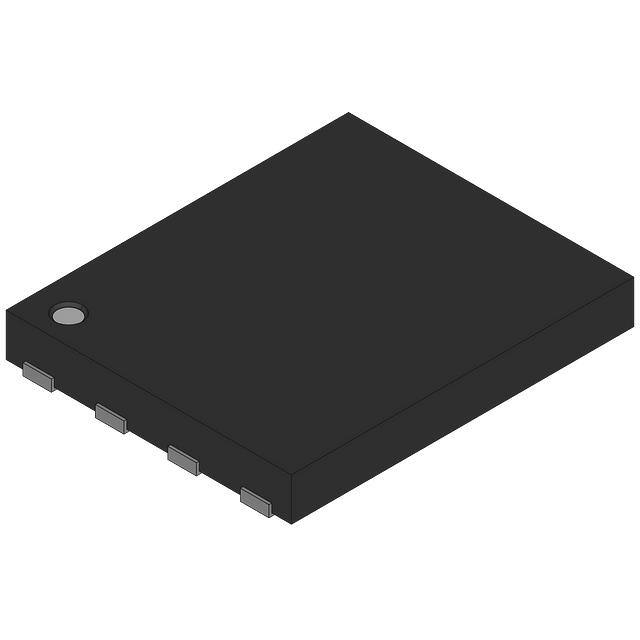
DFN8, 2x2
CASE 506CC
MARKING DIAGRAM
Portable Electronics and Systems
Notebook and Tablet Computers
Telecom, Networking, Medical, and Industrial Equipment
Set−Top Boxes, Servers, and Gateways
Hot Swap Devices and Peripheral Ports
VCC
Bandgap
&
Biases
Charge
Pump
6A
*IMAX_DC is defined as the maximum steady state
current the load switch can pass at room ambient
temperature without entering thermal lockout.
Typical Applications
•
•
•
•
•
IMAX_DC*
EN
1
XX MG
G
XX = 4H for NCP45524−H
= 4L for NCP45524−L
= 5H for NCP45525−H
= 5L for NCP45525−L
M = Date Code
G
= Pb−Free Package
(Note: Microdot may be in either location)
VIN
PG*
Control
Logic
PIN CONFIGURATION
Delay and
Slew Rate
Control
SR*
VIN
1
8
VOUT
EN
2
7
VOUT
VCC
3
6
PG or SR
GND
4
5
BLEED
9: VIN
GND
BLEED
VOUT
(Top View)
Figure 1. Block Diagram
(*Note: either PG or SR available for each part)
ORDERING INFORMATION
See detailed ordering and shipping information on page 14 of
this data sheet.
© Semiconductor Components Industries, LLC, 2016
March, 2020 − Rev. 6
1
Publication Order Number:
NCP45524/D
�NCP45524, NCP45525
Table 1. PIN DESCRIPTION
Pin
Name
Function
1, 9
VIN
Drain of MOSFET (0.5 V – 13.5 V), Pin 1 must be connected to Pin 9
2
EN
NCP45524−H & NCP45525−H − Active−high digital input used to turn on the MOSFET, pin
has an internal pull down resistor to GND
NCP45524−L & NCP45525−L − Active−low digital input used to turn on the MOSFET, pin has
an internal pull up resistor to VCC
3
VCC
Supply voltage to controller (3.0 V − 5.5 V)
4
GND
Controller ground
5
BLEED
Load bleed connection; must be tied to VOUT either directly or through a resistor ≤ 100 MW.
6
PG
NCP45524 − Active−high, open−drain output that indicates when the gate of the MOSFET is
fully charged, external pull up resistor ≥ 1 kW to an external voltage source required; tie to
GND if not used
SR
NCP45525 − Slew rate adjustment; float if not used
7, 8
VOUT
Source of MOSFET connected to load
Table 2. ABSOLUTE MAXIMUM RATINGS
Rating
Symbol
Value
Unit
VCC
−0.3 to 6
V
Supply Voltage Range
Input Voltage Range
VIN
−0.3 to 18
V
Output Voltage Range
VOUT
−0.3 to 18
V
EN Digital Input Range
VEN
−0.3 to (VCC + 0.3)
V
PG Output Voltage Range (Note 1)
VPG
−0.3 to 6
V
Thermal Resistance, Junction−to−Ambient, Steady State (Note 2)
RθJA
40.0
°C/W
Thermal Resistance, Junction−to−Ambient, Steady State (Note 3)
RθJA
72.7
°C/W
Thermal Resistance, Junction−to−Case (VIN Paddle)
RθJC
5.3
°C/W
Continuous MOSFET Current @ TA = 25°C
IMAX
6.0
A
IMAX_TRANS
24
A
Total Power Dissipation @ TA = 25°C (Notes 2 and 4)
Derate above TA = 25°C
PD
2.50
24.9
W
mW/°C
Total Power Dissipation @ TA = 25°C (Notes 3 and 4)
Derate above TA = 25°C
PD
1.37
13.8
W
mW/°C
Storage Temperature Range
TSTG
−40 to 150
°C
Lead Temperature, Soldering (10 sec.)
TSLD
260
°C
ESD Capability, Human Body Model (Notes 5 and 6)
ESDHBM
3.0
kV
ESD Capability, Machine Model (Note 5)
ESDMM
200
V
ESD Capability, Charged Device Model (Note 5)
ESDCDM
1.0
kV
LU
100
mA
Transient MOSFET Current (for up to 500 ms)
Latch−up Current Immunity (Notes 5 and 6)
Stresses exceeding those listed in the Maximum Ratings table may damage the device. If any of these limits are exceeded, device functionality
should not be assumed, damage may occur and reliability may be affected.
1. NCP45524 only. PG is an open−drain output that requires an external pull up resistor ≥ 1 kW to an external voltage source.
2. Surface−mounted on FR4 board using 1 sq−in pad, 1 oz Cu.
3. Surface−mounted on FR4 board using the minimum recommended pad size, 1 oz Cu.
4. Specified for derating purposes only, ensure that IMAX is never exceeded.
5. Tested by the following methods @ TA = 25°C:
ESD Human Body Model tested per JESD22−A114
ESD Machine Model tested per JESD22−A115
ESD Charged Device Model tested per JESD22−C101
Latch−up Current tested per JESD78
6. Rating is for all pins except for VIN and VOUT which are tied to the internal MOSFET’s Drain and Source. Typical MOSFET ESD performance
for VIN and VOUT should be expected and these devices should be treated as ESD sensitive.
www.onsemi.com
2
�NCP45524, NCP45525
Table 3. RECOMMENDED OPERATING RANGES
Rating
Symbol
Min
Max
Unit
Supply Voltage
VCC
3
5.5
V
Input Voltage
VIN
0.5
13.5
V
0
V
Ground
GND
Ambient Temperature
TA
−40
85
°C
Junction Temperature
TJ
−40
125
°C
ETRANS
0
100
mJ
OFF to ON Transition Energy Dissipation Limit (See application section)
Functional operation above the stresses listed in the Recommended Operating Ranges is not implied. Extended exposure to stresses beyond
the Recommended Operating Ranges limits may affect device reliability.
Table 4. ELECTRICAL CHARACTERISTICS (TJ = 25°C unless otherwise specified)
Parameter
Conditions (Note 7)
Symbol
Min
Typ
Max
Unit
18.0
24.0
mW
VCC = 3.3 V; VIN = 5 V
18.8
25.0
VCC = 3.3 V; VIN = 12 V
21.9
31.7
MOSFET
On−Resistance
Leakage Current (Note 8)
VCC = 3.3 V; VIN = 1.8 V
RON
VEN = 0 V; VIN = 13.5 V
ILEAK
0.1
1
mA
VEN = 0 V; VCC = 3 V
ISTBY
0.65
2
mA
3.2
4.5
IDYN
180
300
475
680
86
115
144
72
97
121
CONTROLLER
Supply Standby Current (Note 9)
VEN = 0 V; VCC = 5.5 V
Supply Dynamic Current (Note 10)
VEN = VCC = 3 V; VIN = 12 V
VEN = VCC = 5.5 V; VIN = 1.8 V
Bleed Resistance
RBLEED
VEN = 0 V; VCC = 3 V
VEN = 0 V; VCC = 5.5 V
2
mA
W
EN Input High Voltage
VCC = 3 V − 5.5 V
VIH
V
EN Input Low Voltage
VCC = 3 V − 5.5 V
VIL
0.8
V
EN Input Leakage Current
NCP45524−H; NCP45525−H; VEN = 0 V
IIL
90
500
nA
NCP45524−L; NCP45525−L; VEN = 5.5 V
IIH
90
500
EN Pull Down Resistance
NCP45524−H; NCP45525−H
RPD
76
100
124
kW
EN Pull Up Resistance
NCP45524−L; NCP45525−L
RPU
76
100
124
kW
PG Output Low Voltage (Note 11)
NCP45524; VCC = 3 V; ISINK = 5 mA
VOL
0.2
V
PG Output Leakage Current (Note 12)
NCP45524; VCC = 3 V; VTERM = 3.3 V
IOH
5
100
nA
Slew Rate Control Constant (Note 13)
NCP45525; VCC = 3 V
KSR
31
38
mA
24
Product parametric performance is indicated in the Electrical Characteristics for the listed test conditions, unless otherwise noted. Product
performance may not be indicated by the Electrical Characteristics if operated under different conditions.
7. VEN shown only for NCP45524−H, NCP45525−H (EN Active−High) unless otherwise specified.
8. Average current from VIN to VOUT with MOSFET turned off.
9. Average current from VCC to GND with MOSFET turned off.
10. Average current from VCC to GND after charge up time of MOSFET.
11. PG is an open-drain output that is pulled low when the MOSFET is disabled.
12. PG is an open-drain output that is not driven when the gate of the MOSFET is fully charged, requires an external pull up resistor ≥ 1 kW to
an external voltage source, VTERM.
13. See Applications Information section for details on how to adjust the slew rate.
www.onsemi.com
3
�NCP45524, NCP45525
Table 5. SWITCHING CHARACTERISTICS (TJ = 25°C unless otherwise specified) (Notes 14 and 15)
Parameter
Conditions
Symbol
Min
Typ
VCC = 3.3 V; VIN = 1.8 V
12.1
SR
VCC = 3.3 V; VIN = 12 V
Output Turn−on Delay (Note 16)
Output Turn−off Delay (Note 16)
Power Good Turn−on Time (Note 17)
Power Good Turn−off Time (Note 17)
13.5
VCC = 5.0 V; VIN = 12 V
13.9
VCC = 3.3 V; VIN = 1.8 V
220
VCC = 5.0 V; VIN = 1.8 V
185
TON
VCC = 3.3 V; VIN = 12 V
270
VCC = 5.0 V; VIN = 12 V
260
VCC = 3.3 V; VIN = 1.8 V
1.2
VCC = 5.0 V; VIN = 1.8 V
0.9
TOFF
VCC = 3.3 V; VIN = 12 V
0.4
VCC = 5.0 V; VIN = 12 V
0.2
VCC = 3.3 V; VIN = 1.8 V
0.91
VCC = 5.0 V; VIN = 1.8 V
1.33
VCC = 5.0 V; VIN = 12 V
1.21
VCC = 3.3 V; VIN = 1.8 V
21
VCC = 5.0 V; VIN = 1.8 V
21
VCC = 5.0 V; VIN = 12 V
15
14. See below figure for Test Circuit and Timing Diagram.
15. Tested with the following conditions: VTERM = VCC; RPG = 100 kW; RL = 10 W; CL = 0.1 mF.
16. Applies to NCP45524 and NCP45525.
17. Applies only to NCP45524.
VTERM
RPG
VIN
PG
NCP4552x−H
GND
VEN
RL
SR
50%
TON
CL
50%
Dt
TOFF
90%
VOUT
VOUT
BLEED
VCC
10%
DV
SR =
TPG,ON
DV
90%
Dt
TPG,OFF
50%
50%
VPG
Figure 2. Switching Characteristics Test Circuit and Timing Diagram
www.onsemi.com
4
ms
ms
ms
15
TPG,OFF
VCC = 3.3 V; VIN = 12 V
EN
kV/s
0.93
TPG,ON
VCC = 3.3 V; VIN = 12 V
OFF ON
Unit
11.9
VCC = 5.0 V; VIN = 1.8 V
Output Slew Rate (Note 16)
Max
ns
�NCP45524, NCP45525
TYPICAL CHARACTERISTICS
(TJ = 25°C unless otherwise specified)
35
22
21
20
19
VCC = 5.5 V
18
17
VIN = 5.0 V
25
VIN = 1.8 V
20
15
4.5
6.5
8.5
10.5
10
−45 −30 −15
12.5
0
15
30
45
60
75
90 105 120
VIN, INPUT VOLTAGE (V)
TJ, JUNCTION TEMPERATURE (°C)
Figure 3. On−Resistance vs. Input Voltage
Figure 4. On−Resistance vs. Temperature
ISTBY, SUPPLY STANDBY CURRENT (mA)
ISTBY, SUPPLY STANDBY CURRENT (mA)
2.5
3.5
3.0
2.5
2.0
1.5
1.0
0.5
3.0
IDYN, SUPPLY DYNAMIC CURRENT (mA)
30
VCC = 3 V
0.5
VIN = 12 V
VCC = 3.3 V
RON, ON−RESISTANCE (mW)
23
3.5
4.0
4.5
5.0
5.5
7
6
5
4
VCC = 5.5 V
3
2
1
VCC = 3 V
0
−45 −30 −15
0
15
30
45
60
75
90 105 120
VCC, SUPPLY VOLTAGE (V)
TJ, JUNCTION TEMPERATURE (°C)
Figure 5. Supply Standby Current vs. Supply
Voltage
Figure 6. Supply Standby Current vs.
Temperature
IDYN, SUPPLY DYNAMIC CURRENT (mA)
RON, ON−RESISTANCE (mW)
24
500
450
400
350
300
250
200
VCC = 5.5 V
150
VCC = 3 V
100
0.5
2.5
4.5
6.5
8.5
10.5
12.5
500
450
VIN = 1.8 V
400
350
300
250
VIN = 12 V
200
150
100
3.0
3.5
4.0
4.5
5.0
5.5
VIN, INPUT VOLTAGE (V)
VCC, SUPPLY VOLTAGE (V)
Figure 7. Supply Dynamic Current vs. Input
Voltage
Figure 8. Supply Dynamic Current vs. Supply
Voltage
www.onsemi.com
5
�NCP45524, NCP45525
TYPICAL CHARACTERISTICS
115
600
RBLEED, BLEED RESISTANCE (W)
700
VCC = 5.5 V, VIN = 1.8 V
500
400
300
VCC = 3.0 V, VIN = 12 V
200
100
−45
15
45
75
100
3.0
3.5
4.0
4.5
5.0
5.5
TJ, JUNCTION TEMPERATURE (°C)
VCC, SUPPLY VOLTAGE (V)
Figure 9. Supply Dynamic Current vs.
Temperature
Figure 10. Bleed Resistance vs. Supply
Voltage
135
VCC = 3 V
125
115
VCC = 5.5 V
105
95
−15
15
45
75
105
120
115
110
105
100
95
90
85
−45
−15
15
45
75
105
TJ, JUNCTION TEMPERATURE (°C)
TJ, JUNCTION TEMPERATURE (°C)
Figure 11. Bleed Resistance vs. Temperature
Figure 12. EN Pull Down/Up Resistance vs.
Temperature
0.140
VOL, PG OUTPUT LOW VOLTAGE (V)
RBLEED, BLEED RESISTANCE (W)
VOL, PG OUTPUT LOW VOLTAGE (V)
105
105
145
85
−45
110
95
−15
IPD/PU, EN PULL DOWN/UP RESISTANCE (kW)
IDYN, SUPPLY DYNAMIC CURRENT (mA)
(TJ = 25°C unless otherwise specified)
ISINK = 5 mA
0.135
0.130
0.125
0.120
0.115
0.110
3.0
3.5
4.0
4.5
5.0
5.5
0.20
ISINK = 5 mA
0.18
VCC = 3 V
0.16
0.14
VCC = 5.5 V
0.12
0.10
0.08
−45
−15
15
45
75
105
VCC, SUPPLY VOLTAGE (V)
TJ, JUNCTION TEMPERATURE (°C)
Figure 13. PG Output Low Voltage vs. Supply
Voltage
Figure 14. PG Output Low Voltage vs.
Temperature
www.onsemi.com
6
�NCP45524, NCP45525
TYPICAL CHARACTERISTICS
KSR, SLEW RATE CONTROL CONSTANT (mA)
KSR, SLEW RATE CONTROL CONSTANT (mA)
(TJ = 25°C unless otherwise specified)
34
33
VCC = 5.5 V
32
VCC = 3 V
31
30
29
0.5
2.5
4.5
6.5
8.5
10.5
12.5
VCC = 5.5 V
33
32
31
VCC = 3 V
30
29
28
−45
−15
15
45
75
105
TJ, JUNCTION TEMPERATURE (°C)
Figure 15. Slew Rate Control Constant vs.
Input Voltage
Figure 16. Slew Rate Control Constant vs.
Temperature
14.0
14
SR, OUTPUT SLEW RATE (kV/s)
SR, OUTPUT SLEW RATE (kV/s)
34
VIN, INPUT VOLTAGE (V)
15
VCC = 5.5 V
13
VCC = 3 V
12
11
10
9
8
0.5
2.5
4.5
6.5
8.5
10.5
VCC = 3.3 V, VIN = 12 V
13.5
13.0
12.5
12.0
VCC = 5 V, VIN = 1.8 V
11.5
11.0
10.5
−40
12.5
−20
0
20
40
60
80
100
120
VIN, INPUT VOLTAGE (V)
TJ, JUNCTION TEMPERATURE (°C)
Figure 17. Output Slew Rate vs. Input Voltage
Figure 18. Output Slew Rate vs. Temperature
310
TON, OUTPUT TURN−ON DELAY (ms)
TON, OUTPUT TURN−ON DELAY (ms)
35
290
270
VCC = 3 V
250
VCC = 5.5 V
230
210
190
170
150
0.5
2.5
4.5
6.5
8.5
10.5
12.5
300
VCC = 3.3 V, VIN = 12 V
275
250
225
200
VCC = 5 V, VIN = 1.8 V
175
150
−40
−20
0
20
40
60
80
100
VIN, INPUT VOLTAGE (V)
TJ, JUNCTION TEMPERATURE (°C)
Figure 19. Output Turn−on Delay vs. Input
Voltage
Figure 20. Output Turn−on Delay vs.
Temperature
www.onsemi.com
7
120
�NCP45524, NCP45525
TYPICAL CHARACTERISTICS
1.8
TOFF, OUTPUT TURN−OFF DELAY (ms)
TOFF, OUTPUT TURN−OFF DELAY (ms)
(TJ = 25°C unless otherwise specified)
1.6
1.4
1.2
1.0
VCC = 3 V
0.8
0.6
VCC = 5.5 V
0.4
0.2
0
0.5
2.5
4.5
6.5
8.5
10.5
12.5
0.8
0.6
VCC = 3.3 V, VIN = 12 V
0.4
0.2
−40
−20
0
20
40
60
80
100
VIN, INPUT VOLTAGE (V)
TJ, JUNCTION TEMPERATURE (°C)
Figure 22. Output Turn−off Delay vs.
Temperature
120
1.5
TPG,ON, PG TURN−ON TIME (ms)
TPG,ON, PG TURN−ON TIME (ms)
VCC = 5 V, VIN = 1.8 V
1.0
Figure 21. Output Turn−off Delay vs. Input
Voltage
1.8
1.7
1.6
1.5
1.4
VCC = 3 V
1.3
1.2
1.1
VCC = 5.5 V
1.0
0.9
0.8
0.5
2.5
4.5
6.5
8.5
10.5
1.4
VCC = 3.3 V, VIN = 12 V
1.3
1.2
1.1
1.0
VCC = 5 V, VIN = 1.8 V
0.9
0.8
−40
12.5
−20
0
20
40
60
80
100
VIN, INPUT VOLTAGE (V)
TJ, JUNCTION TEMPERATURE (°C)
Figure 23. Power Good Turn−on Time vs. Input
Voltage
Figure 24. Power Good Turn−on Time vs.
Temperature
120
27.5
TPG,OFF, PG TURN−OFF TIME (ns)
24
TPG,OFF, PG TURN−OFF TIME (ns)
1.2
22
VIN = 13.5 V
20
VIN = 0.5 V
18
16
14
3.5
4.0
4.5
5.0
VCC = 3.3 V, VIN = 12 V
22.5
20.0
17.5
VCC = 5 V, VIN = 1.8 V
15.0
12.5
10.0
−40 −20
12
3.0
25.0
5.5
0
20
40
60
80
100
VCC, SUPPLY VOLTAGE (V)
TJ, JUNCTION TEMPERATURE (°C)
Figure 25. Power Good Turn−off Time vs.
Supply Voltage
Figure 26. Power Good Turn−off Time vs.
Temperature
www.onsemi.com
8
120
�NCP45524, NCP45525
TYPICAL CHARACTERISTICS
(TJ = 25°C unless otherwise specified)
ID, DRAIN CURRENT (A)
100
10 ms
100 ms
10
1
0.1
0.01
TA = 85°C
TJ = 125°C
0 V ≤ VGS ≤ 6 V
Single Pulse
RDS(on) Limit
Thermal Limit
Package Limit
0.1
1 ms
10 ms
100 ms
1
10
VDS, DRAIN−TO−SOURCE VOLTAGE (V)
Figure 27. Maximum Rated Forward Biased
Safe Operating Area
www.onsemi.com
9
100
�NCP45524, NCP45525
APPLICATIONS INFORMATION
Enable Control
than or equal to 1 kW to an external voltage source, VTERM,
that is compatible with input levels of all devices connected
to this pin (as shown in Figures 28 and 29).
The power good output can be used as the enable signal for
other active−high devices in the system (as shown in
Figure 30). This allows for guaranteed by design power
sequencing and reduces the number of enable signals needed
from the system controller. If the power good feature is not
used in the application, the PG pin should be tied to GND.
Both the NCP45524 and the NCP45525 have two part
numbers, NCP4552x-H and NCP4552x-L, that only differ
in the polarity of the enable control.
The NCP4552x-H devices allow for enabling the
MOSFET in an active-high configuration. When the VCC
supply pin has an adequate voltage applied and the EN pin
is at a logic high level, the MOSFET will be enabled.
Similarly, when the EN pin is at a logic low level, the
MOSFET will be disabled. An internal pull down resistor to
ground on the EN pin ensures that the MOSFET will be
disabled when not being driven.
The NCP4552x-L devices allow for enabling the
MOSFET in an active-low configuration. When the VCC
supply pin has an adequate voltage applied and the EN pin
is at a logic low level, the MOSFET will be enabled.
Similarly, when the EN pin is at a logic high level, the
MOSFET will be disabled. An internal pull up resistor to
VCC on the EN pin ensures that the MOSFET will be
disabled when not being driven.
Slew Rate Control
The NCP4552x devices are equipped with controlled
output slew rate which provides soft start functionality. This
limits the inrush current caused by capacitor charging and
enables these devices to be used in hot swap applications.
The slew rate of the NCP45525 can be decreased with an
external capacitor added between the SR pin and ground (as
shown in Figures 31 and 32). With an external capacitor
present, the slew rate can be determined by the following
equation:
Slew Rate +
Power Sequencing
K SR
[Vńs]
C SR
(eq. 1)
The NCP4552x devices will function with any power
sequence, but the output turn−on delay performance may
vary from what is specified. To achieve the specified
performance, there are two recommended power sequences:
1) VCC → VIN → VEN
2) VIN → VCC → VEN
VCC must be at 2 V or higher when EN is asserted to ensure
that the enable is latched properly for correct operation. If
EN comes up before VCC reaches 2 V, then the EN may not
take effect.
where KSR is the specified slew rate control constant, found
in Table 4, and CSR is the slew rate control capacitor added
between the SR pin and ground. The slew rate of the device
will always be the lower of the default slew rate and the
adjusted slew rate. Therefore, if the CSR is not large enough
to decrease the slew rate more than the specified default
value, the slew rate of the device will be the default value.
The SR pin can be left floating if the slew rate does not need
to be decreased.
Load Bleed (Quick Discharge)
Capacitive Load
The NCP4552x devices have an internal bleed resistor,
RBLEED, which is used to bleed the charge off of the load to
ground after the MOSFET has been disabled. In series with
the bleed resistor is a bleed switch that is enabled whenever
the MOSFET is disabled. The MOSFET and the bleed
switch are never concurrently active.
Is it required that the BLEED pin be connected to VOUT
either directly (as shown in Figures 29 and 32) or through an
external resistor, REXT (as shown in Figures 28 and 31).
REXT should not exceed 100 MW and can be used to increase
the total bleed resistance and decrease the load bleed rate.
Care must be taken to ensure that the power dissipated
across RBLEED is kept at a safe level. The maximum
continuous power that can be dissipated across RBLEED is
0.4 W. REXT can be used to decrease the amount of power
dissipated across RBLEED.
The peak in−rush current associated with the initial
charging of the application load capacitance needs to stay
below the specified IMAX. CL (capacitive load) should be
less than Cmax as defined by the following equation:
C max +
I max
SR typ
(eq. 2)
Where IMAX is the maximum load current, and SRtyp is the
typical default slew rate when no external load capacitor is
added to the SR pin.
OFF to ON Transition Energy Dissipation
The energy dissipation due to load current traveling from
VIN to VOUT is very low during steady state operation due
to the low RON. When the EN signal is asserted high, the load
switch transitions from an OFF state to an ON state. During
this time, the resistance from VIN to VOUT transitions from
high impedance to RON, and additional energy is dissipated
in the device for a short period of time. The worst case
energy dissipated during the OFF to ON transition can be
approximated by the following equation:
Power Good
The NCP45524 devices have a power good output (PG)
that can be used to indicate when the gate of the MOSFET
is fully charged. The PG pin is an active-high, open-drain
output that requires an external pull up resistor, RPG, greater
www.onsemi.com
10
�NCP45524, NCP45525
E + 0.5 @ V IN @ ǒI INRUSH ) 0.8 @ I LOADǓ @ dt
Power Planes: The ecoSWITCH is optimized for extremely
low Ron resistance, however, improper PCB layout can
substantially increase source to load series resistance by
adding PCB board parasitic resistance. Solid connections to
the VIN and VOUT pins of the ecoSWITCH to copper
planes should be used to achieve low series resistance and
good thermal dissipation. The ecoSWITCH requires ample
heat dissipation for correct thermal lockout operation. The
internal FET dissipates load condition dependent amounts
of power in the milliseconds following the rising edge of
enable, and providing good thermal conduction from the
packaging to the board is critical. Direct coupling of VIN to
VOUT should be avoided, as this will adversely affect slew
rates. The figure below shows an example of correct power
plane layout. The number and location of pins for specific
ecoSWITCH products may vary. This demonstrates large
planes for both VIN and VOUT, while avoiding capacitive
coupling between the two planes.
(eq. 3)
Where VIN is the voltage on the VIN pin, IINRUSH is the
inrush current caused by capacitive loading on VOUT, and dt
is the time it takes VOUT to rise from 0 V to VIN. IINRUSH can
be calculated using the following equation:
I INRUSH + dv @ C L
dt
(eq. 4)
Where dv/dt is the programmed slew rate, and CL is the
capacitive loading on VOUT. To prevent thermal lockout or
damage to the device, the energy dissipated during the OFF
to ON transition should be limited to ETRANS listed in
operating ranges table.
ecoSWITCH LAYOUT GUIDELINES
Electrical Layout Considerations
Correct physical PCB layout is important for proper low
noise accurate operation of all ecoSWITCH products.
VTERM = 3.3 V
RPG
100 kW
3.0 V − 5.5 V
Power Supply
or Battery
0.5 V − 13.5 V
Controller
VCC
EN
VIN
PG
Bandgap
&
Biases
Control
Logic
Charge
Pump
Delay and
Slew Rate
Control
GND
BLEED
VOUT
REXT
Load
Figure 28. NCP45524 Typical Application Diagram − Load Switch
www.onsemi.com
11
�NCP45524, NCP45525
VCC
3.0 V − 5.5 V
PG VTERM
EN
GND
VIN
0.5 V − 13.5 V
RPG
BACKPLANE
REMOVABLE
CARD
VCC
EN
VIN
PG
Bandgap
&
Biases
Control
Logic
Charge
Pump
Delay and
Slew Rate
Control
GND
VOUT
BLEED
Load
Figure 29. NCP45524 Typical Application Diagram − Hot Swap
VTERM = 3.3 V
EN
PG
EN
PG
RPG
10 kW
Controller
RPD
100 kW
RPD
100 kW
PG
PG
NCP45524−H
NCP45524−H
Figure 30. NCP45524 Simplified Application Diagram − Power Sequencing with PG Output
www.onsemi.com
12
�NCP45524, NCP45525
Power Supply
or Battery
3.0 V − 5.5 V
Controller
0.5 V − 13.5 V
EN
VCC
VIN
Bandgap
&
Biases
Control
Logic
Charge
Pump
Delay and
Slew Rate
Control
SR
GND
BLEED
CSR
VOUT
REXT
Load
Figure 31. NCP45525 Typical Application Diagram − Load Switch
VCC
3.0 V − 5.5 V
GND
EN
VIN
0.5 V − 13.5 V
BACKPLANE
REMOVABLE
CARD
VCC
EN
Bandgap
&
Biases
Control
Logic
Charge
Pump
Delay and
Slew Rate
Control
VIN
SR
GND
BLEED
VOUT
CSR
Load
Figure 32. NCP45525 Typical Application Diagram − Hot Swap
www.onsemi.com
13
�NCP45524, NCP45525
ORDERING INFORMATION
Device
Pin 6 Functionality
EN Polarity
NCP45524IMNTWG−H
PG
Active−High
NCP45524IMNTWG−L
PG
Active−Low
NCP45525IMNTWG−H
SR
Active−High
NCP45525IMNTWG−L
SR
Active−Low
Package
Shipping†
DFN8
(Pb−Free)
3000 / Tape & Reel
†For information on tape and reel specifications, including part orientation and tape sizes, please refer to our Tape and Reel Packaging
Specifications Brochure, BRD8011/D.
ecoSWITCH is a trademark of Semiconductor Components Industries, LLC (SCILLC).
www.onsemi.com
14
�MECHANICAL CASE OUTLINE
PACKAGE DIMENSIONS
DFN8 2x2, 0.5P
CASE 506CC
ISSUE A
1
SCALE 2:1
A
D
PIN ONE
REFERENCE
2X
B
L
ÇÇ
ÇÇ
0.10 C
DETAIL A
ALTERNATE
CONSTRUCTIONS
TOP VIEW
DETAIL B
EXPOSED Cu
A
A3
A1
A1
SIDE VIEW
NOTE 4
DETAIL A
1
D2
4
C
8
5
0.10 C A B
0.05 C
1.70
XX MG
G
(Note: Microdot may be in either location)
*This information is generic. Please refer to
device data sheet for actual part marking.
Pb−Free indicator, “G” or microdot “ G”,
may or may not be present.
NOTE 3
RECOMMENDED
SOLDERING FOOTPRINT*
PACKAGE
OUTLINE
MILLIMETERS
MIN
MAX
0.80
1.00
0.00
0.05
0.20 REF
0.20
0.30
2.00 BSC
1.50
1.70
2.00 BSC
0.80
1.00
0.50 BSC
0.20 REF
0.18
0.38
−−−
0.15
0.14 REF
XX = Specific Device Code
M = Date Code
G
= Pb−Free Package
K
b
BOTTOM VIEW
DIM
A
A1
A3
b
D
D2
E
E2
e
K
L
L1
M
1
8X
e
e/2
A3
NOTES:
1. DIMENSIONING AND TOLERANCING PER
ASME Y14.5M, 1994.
2. CONTROLLING DIMENSION: MILLIMETERS.
3. DIMENSION b APPLIES TO PLATED
TERMINAL AND IS MEASURED BETWEEN
0.15 AND 0.30 MM FROM TERMINAL TIP.
4. COPLANARITY APPLIES TO THE EXPOSED
PAD AS WELL AS THE TERMINALS.
GENERIC
MARKING DIAGRAM*
L
8X
DETAIL B
ALTERNATE
CONSTRUCTION
SEATING
PLANE
E2
M
ÇÇ
ÇÇ
ÉÉ
MOLD CMPD
0.10 C
0.08 C
L
L1
E
0.10 C
2X
DATE 24 JUN 2014
8X
0.50
0.20
2.30
1.00
1
8X
0.50
PITCH
0.30
DIMENSIONS: MILLIMETERS
*For additional information on our Pb−Free strategy and soldering
details, please download the ON Semiconductor Soldering and
Mounting Techniques Reference Manual, SOLDERRM/D.
DOCUMENT NUMBER:
DESCRIPTION:
98AON67172E
DFN8 2X2, 0.5P
Electronic versions are uncontrolled except when accessed directly from the Document Repository.
Printed versions are uncontrolled except when stamped “CONTROLLED COPY” in red.
PAGE 1 OF 1
ON Semiconductor and
are trademarks of Semiconductor Components Industries, LLC dba ON Semiconductor or its subsidiaries in the United States and/or other countries.
ON Semiconductor reserves the right to make changes without further notice to any products herein. ON Semiconductor makes no warranty, representation or guarantee regarding
the suitability of its products for any particular purpose, nor does ON Semiconductor assume any liability arising out of the application or use of any product or circuit, and specifically
disclaims any and all liability, including without limitation special, consequential or incidental damages. ON Semiconductor does not convey any license under its patent rights nor the
rights of others.
© Semiconductor Components Industries, LLC, 2019
www.onsemi.com
�onsemi,
, and other names, marks, and brands are registered and/or common law trademarks of Semiconductor Components Industries, LLC dba “onsemi” or its affiliates
and/or subsidiaries in the United States and/or other countries. onsemi owns the rights to a number of patents, trademarks, copyrights, trade secrets, and other intellectual property.
A listing of onsemi’s product/patent coverage may be accessed at www.onsemi.com/site/pdf/Patent−Marking.pdf. onsemi reserves the right to make changes at any time to any
products or information herein, without notice. The information herein is provided “as−is” and onsemi makes no warranty, representation or guarantee regarding the accuracy of the
information, product features, availability, functionality, or suitability of its products for any particular purpose, nor does onsemi assume any liability arising out of the application or use
of any product or circuit, and specifically disclaims any and all liability, including without limitation special, consequential or incidental damages. Buyer is responsible for its products
and applications using onsemi products, including compliance with all laws, regulations and safety requirements or standards, regardless of any support or applications information
provided by onsemi. “Typical” parameters which may be provided in onsemi data sheets and/or specifications can and do vary in different applications and actual performance may
vary over time. All operating parameters, including “Typicals” must be validated for each customer application by customer’s technical experts. onsemi does not convey any license
under any of its intellectual property rights nor the rights of others. onsemi products are not designed, intended, or authorized for use as a critical component in life support systems
or any FDA Class 3 medical devices or medical devices with a same or similar classification in a foreign jurisdiction or any devices intended for implantation in the human body. Should
Buyer purchase or use onsemi products for any such unintended or unauthorized application, Buyer shall indemnify and hold onsemi and its officers, employees, subsidiaries, affiliates,
and distributors harmless against all claims, costs, damages, and expenses, and reasonable attorney fees arising out of, directly or indirectly, any claim of personal injury or death
associated with such unintended or unauthorized use, even if such claim alleges that onsemi was negligent regarding the design or manufacture of the part. onsemi is an Equal
Opportunity/Affirmative Action Employer. This literature is subject to all applicable copyright laws and is not for resale in any manner.
PUBLICATION ORDERING INFORMATION
LITERATURE FULFILLMENT:
Email Requests to: orderlit@onsemi.com
onsemi Website: www.onsemi.com
◊
TECHNICAL SUPPORT
North American Technical Support:
Voice Mail: 1 800−282−9855 Toll Free USA/Canada
Phone: 011 421 33 790 2910
Europe, Middle East and Africa Technical Support:
Phone: 00421 33 790 2910
For additional information, please contact your local Sales Representative
�