ON Semiconductor
Is Now
To learn more about onsemi™, please visit our website at
www.onsemi.com
onsemi and and other names, marks, and brands are registered and/or common law trademarks of Semiconductor Components Industries, LLC dba “onsemi” or its affiliates and/or
subsidiaries in the United States and/or other countries. onsemi owns the rights to a number of patents, trademarks, copyrights, trade secrets, and other intellectual property. A listing of onsemi
product/patent coverage may be accessed at www.onsemi.com/site/pdf/Patent-Marking.pdf. onsemi reserves the right to make changes at any time to any products or information herein, without
notice. The information herein is provided “as-is” and onsemi makes no warranty, representation or guarantee regarding the accuracy of the information, product features, availability, functionality,
or suitability of its products for any particular purpose, nor does onsemi assume any liability arising out of the application or use of any product or circuit, and specifically disclaims any and all
liability, including without limitation special, consequential or incidental damages. Buyer is responsible for its products and applications using onsemi products, including compliance with all laws,
regulations and safety requirements or standards, regardless of any support or applications information provided by onsemi. “Typical” parameters which may be provided in onsemi data sheets and/
or specifications can and do vary in different applications and actual performance may vary over time. All operating parameters, including “Typicals” must be validated for each customer application
by customer’s technical experts. onsemi does not convey any license under any of its intellectual property rights nor the rights of others. onsemi products are not designed, intended, or authorized
for use as a critical component in life support systems or any FDA Class 3 medical devices or medical devices with a same or similar classification in a foreign jurisdiction or any devices intended for
implantation in the human body. Should Buyer purchase or use onsemi products for any such unintended or unauthorized application, Buyer shall indemnify and hold onsemi and its officers, employees,
subsidiaries, affiliates, and distributors harmless against all claims, costs, damages, and expenses, and reasonable attorney fees arising out of, directly or indirectly, any claim of personal injury or death
associated with such unintended or unauthorized use, even if such claim alleges that onsemi was negligent regarding the design or manufacture of the part. onsemi is an Equal Opportunity/Affirmative
Action Employer. This literature is subject to all applicable copyright laws and is not for resale in any manner. Other names and brands may be claimed as the property of others.
�NCP5901
VR12 Compatible
Synchronous Buck MOSFET
Drivers
The NCP5901 is a high performance dual MOSFET gate driver
optimized to drive the gates of both high−side and low−side power
MOSFETs in a synchronous buck converter. It can drive up to 3 nF
load with a 25 ns propagation delay and 20 ns transition time.
Adaptive anti−cross−conduction and power saving operation
circuit can provide a low switching loss and high efficiency solution
for notebook and desktop systems. Bidirectional EN pin can provide
a fault signal to controller when the gate driver fault detect under
OVP, UVLO occur. Also, an under−voltage lockout function
guarantees the outputs are low when supply voltage is low.
http://onsemi.com
8
1
1
SOIC−8 NB
D SUFFIX
CASE 751
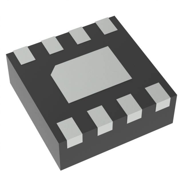
DFN8
MN SUFFIX
CASE 506AA
Features
•
•
•
•
•
•
•
•
•
•
•
Faster Rise and Fall Times
Adaptive Anti−Cross−Conduction Circuit
Pre OV function
ZCD Detect
Floating Top Driver Accommodates Boost Voltages of up to 35 V
Output Disable Control Turns Off Both MOSFETs
Under−voltage Lockout
Power Saving Operation Under Light Load Conditions
Direct Interface to NCP6151 and Other Compatible PWM
Controllers
Thermally Enhanced Package
These are Pb−Free Devices
MARKING DIAGRAMS
8
N5901
ALYW
G
1
N5901
A
L
Y
W
G
= Specific Device Code
= Assembly Location
= Wafer Lot
= Year
= Work Week
= Pb−Free Package
1
Typical Applications
• Power Solutions for Desktop Systems
AJ
M
G
AJMG
G
= Specific Device Code
= Date Code
= Pb−Free Device
ORDERING INFORMATION
Device
Package
Shipping†
NCP5901MNTBG
DFN8
3000 / Tape & Reel
(Pb−Free)
NCP5901DR2G
SOIC−8 2500 / Tape & Reel
(Pb−Free)
†For information on tape and reel specifications,
including part orientation and tape sizes, please
refer to our Tape and Reel Packaging Specification
Brochure, BRD8011/D.
© Semiconductor Components Industries, LLC, 2013
June, 2013 − Rev. 2
1
Publication Order Number:
NCP5901/D
�NCP5901
BST
DRVH
1
PWM
SW
FLAG
9
EN
GND
VCC
DRVL
(Top View)
Figure 1. Pin Diagram
BST
VCC
DRVH
PWM
Logic
SW
Anti−Cross
Conduction
VCC
DRVL
EN
Fault
ZCD
Detection
UVLO
Pre−OV
Figure 2. Block Diagram
Table 1. Pin Descriptions
Pin No.
Symbol
Description
1
BST
Floating bootstrap supply pin for high side gate driver. Connect the bootstrap capacitor between this pin
and the SW pin.
2
PWM
Control input. The PWM signal has three distinctive states: Low = Low Side FET Enabled, Mid = Diode
Emulation Enabled, High = High Side FET Enabled.
3
EN
4
VCC
Power supply input. Connect a bypass capacitor (0.1 mF) from this pin to ground.
5
DRVL
Low side gate drive output. Connect to the gate of low side MOSFET.
6
GND
Bias and reference ground. All signals are referenced to this node (QFN Flag).
7
SW
8
DRVH
High side gate drive output. Connect to the gate of high side MOSFET.
9
FLAG
Thermal flag. There is no electrical connection to the IC. Connect to ground plane.
Logic input. A logic high to enable the part and a logic low to disable the part.
Switch node. Connect this pin to the source of the high side MOSFET and drain of the low side MOSFET.
http://onsemi.com
2
�NCP5901
12V_POWER
CR1
MMSD4148
R164
R1
1.02
R143
0.0
TP4
PWM
TP1
C4
0.027uF
EN
C2
4.7uF
TP5
+
CE9
390uF
TP6
GND
235nH
TP7
Q9
NTMFS4851N
VREG_SW1_LG
LG
VCCP
L
VREG_SW1_OUT
Q10
NTMFS4851N
R3
2.2
JP13_ETCH CSN11
PAD
TP8
C5
1uF
C3
4.7uF
0.0
VREG_SW1_HG
HG
VCC
C1
4.7uF
R142
PWM SW
DRON
TP2
0.0
NCP5901 TP3
BST
Q1
NTMFS4821N
C6
2700pF
JP14_ETCH CSP11
Figure 3. Application Circuit
Table 2. ABSOLUTE MAXIMUM RATINGS
Pin Symbol
Pin Name
VMAX
VMIN
VCC
Main Supply Voltage Input
15 V
−0.3 V
BST
Bootstrap Supply Voltage
35 V wrt/ GND
40 V ≤ 50 ns wrt/ GND
15 V wrt/ SW
−0.3 V wrt/SW
SW
Switching Node
(Bootstrap Supply Return)
35 V
40 V ≤ 50 ns
−5 V
−10 V (200 ns)
DRVH
High Side Driver Output
BST+0.3 V
−0.3 V wrt/SW
−2 V (