NCS2561, NCV2561
Video Amplifier, 1-Channel,
With Reconstruction Filter
and SAG Correction
The NCS2561 is a single high speed video driver including a 2−pole
reconstruction filter and SAG correction capability. The NCS2561 is
available in a space saving SC−88 package optimized for low voltage,
portable applications. It is designed to be compatible with
Digital−to−Analog Converters (DAC) embedded in most video processors.
The NCS2561 internally integrates an 8 MHz 2−pole video DAC
reconstruction filter with a fixed gain of 2. The NCS2561 also has a
built−in SAG correction circuit when used at the output in an AC
−coupled mode. To further reduce power consumption, an enable pin
is provided.
www.onsemi.com
MARKING
DIAGRAMS
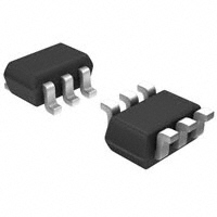
6
1
SC−88
SQ SUFFIX
CASE 419B
YG1 MG
G
1
Features
•
•
•
•
•
•
•
•
•
•
•
•
Internal 8 MHz 2−Pole Reconstruction Filter
Internal Fixed Gain: 6 dB
Integrated Level Shifter
SAG Correction Circuit for Reducing Coupling Capacitor Size
Low Quiescent Current: 6 mA Typ
Shutdown Current < 5 mA
Wide Input Voltage Range
Capability to Drive 2 CVBS Video Signals Together (2x150W Loads)
Excellent Video Performance
Operating Supply Voltage Range: +2.7 V to +3.3 V
NCV Prefix for Automotive and Other Applications Requiring
Unique Site and Control Change Requirements; AEC−Q100
Qualified and PPAP Capable
These Devices are Pb−Free and are RoHS Compliant
Applications
Enable
6
5
NCS2561
IN
Level
Shifter
2−pole
filter
PIN CONNECTIONS
1
6
2
5
3
4
IN
VCC
GND
Enable
SAG
OUT
Top View
Device
Package
Shipping†
NCS2561SQT1G
SC−88 3000 / Tape & Reel
(Pb−Free)
NCV2561SQT1G
SC−88 3000 / Tape & Reel
(Pb−Free)
†For information on tape and reel specifications,
including part orientation and tape sizes, please
refer to our Tape and Reel Packaging Specifications
Brochure, BRD8011/D.
+
1
(Note: Microdot may be in either location)
*Date Code orientation and/or position may
vary depending upon manufacturing location.
ORDERING INFORMATION
• Portable Video, Digital Cameras & Camera Phones
• Set−Top Box Video Filters
• NTSC and PAL
Vcc
2.7V to 3.3V
YG1 = Specific Device Code
M
= Date Code*
G
= Pb−Free Package
4
OUT
3
SAG
−
Related Resource:
Refer to Application Note AND8457/D for details
regarding SAG Correction
2
GND
Figure 1. Block Diagram
© Semiconductor Components Industries, LLC, 2011
August, 2018 − Rev. 4
1
Publication Order Number:
NCS2561/D
�NCS2561, NCV2561
PIN FUNCTION AND DESCRIPTION
Pin
Name
Type
Description
1
IN
Input
2
GND
Ground
Ground
3
SAG
Output
Sag Compensation
4
OUT
Output
Video Output
5
Enable
Input
6
VCC
Power
Video Input
Enable / Disable Function: High = Enable, Low = Disable. When left open the default state is High.
Power Supply / 2.7 V ≤ VCC ≤ 3.3 V
ATTRIBUTES
Characteristic
ESD Protection (Note 1)
Value
Human Body Model
Machine Model
2 kV
200 V
Latch−up Current (Note 2)
75 mA
Moisture Sensitivity (Note 3)
Level 1
Flammability Rating
Oxygen Index: 28 to 34
UL 94 V−0 @ 0.125 in
1. This device series incorporates ESD protection and is tested by the following methods:
ESD Human Body Model tested per JEDEC standard JS−001−2017 (AEC−Q100−002)
ESD Charged Device Model tested per JEDEC standard JS−002−2014 (AEC−Q100−011).
2. Latch−up Current tested per JEDEC standard JESD78E (AEC−Q100−004).
3. For additional Moisture Sensitivity information, refer to Application Note AND8003/D.
MAXIMUM RATINGS
Rating
Symbol
Value
Unit
VCC
3.6
Vdc
Input Voltage Range
VI
−0.5 to VCC + 0.5
Vdc
Output Short−Circuit to GND thru 75 W
ISC
Continuous
−
Maximum Junction Temperature (Note 4)
TJ
150
°C
TA
−40 to +125
−40 to +125
°C
Storage Temperature Range
Tstg
−60 to +150
°C
Thermal Resistance, Junction−to−Air
RqJA
250
°C/W
Power Supply Voltages
Operating Ambient Temperature
NCS2561
NCV2561 (Note 5)
Stresses exceeding those listed in the Maximum Ratings table may damage the device. If any of these limits are exceeded, device functionality
should not be assumed, damage may occur and reliability may be affected.
4. Power dissipation must be considered to ensure maximum junction temperature (TJ) is not exceeded.
5. NCV prefix is for automotive and other applications requiring site and change control.
MAXIMUM POWER DISSIPATION
The maximum power that can be safely dissipated is
limited by the associated rise in junction temperature. For
the plastic packages, the maximum safe junction
temperature is 150°C. If the maximum is exceeded
momentarily, proper circuit operation will be restored as
soon as the die temperature is reduced. Leaving the device
in the “overheated” condition for an extended period can
result in device burnout. To ensure proper operation, it is
important to observe the de−rating curves.
www.onsemi.com
2
�NCS2561, NCV2561
DC ELECTRICAL CHARACTERISTICS with VCC = 2.7 V to 3.3 V (TA = +25°C, RL = 150 W to GND, unless otherwise specified)
Characteristic
Symbol
Conditions
Min
Typ
Max
Unit
VCC = 3.3 V, VIN = 0 V
10
60
60
80
mV
DC PERFORMANCE
VOLS
Offset Level−Shift Output Voltage
TA = −40°C to +125°C (Note 6)
IIB
Input Bias Current
VIN
Input Voltage Range (Note 7)
AV
Voltage Gain
VIH
Enable Input High Level Voltage
VIL
Enable Input Low Level Voltage
±3
VCC = 3.3 V
GND
VCC = 3.3 V, 0 < VIN < 1.5 V
40 IRE Sync,
100 IRE White Level
5.8
pA
VCC − 1.5
V
6.2
dB
1.6
VCC
V
GND
0.8
V
6.0
OUTPUT CHARACTERISTICS
VOH
Output High Level Voltage
VOL
Output Low Level Voltage
(Note 8)
IO
Output Current
RL = 150 W to GND
RL = 75 W to GND
VCC − 0.3
VCC = 3.3 V
VCC − 0.1
VCC − 0.3
V
60
mV
±50
mA
POWER SUPPLY
VCC
Operating Voltage Range
2.7
3.3
V
ICC, ON
Power Supply Current − Enabled
TA = −40°C to +125°C (Note 6)
VIN = 0 V, VCC = 3.3 V, IO = 0 mA
6.0
7.5
9.0
mA
ICC,
Power Supply Current − Disabled
VIN = 0 V, VCC = 3.3 V, IO = 0 mA
1.5
5.0
mA
VCC = 2.7 V to 3.3 V
±80
OFF
PSRR
Power Supply Rejection Ratio
mV/V
6. Guaranteed by design and/or characterization.
7. Limited by output swing and internal gain.
8. Output low voltage level is limited by the internal level shift circuitry.
AC ELECTRICAL CHARACTERISTICS with VCC = 2.7 V to 3.3 V (TA = +25°C, RL = 150 W to GND, unless otherwise specified)
Symbol
Characteristic
Conditions
Min
Typ
Max
Unit
−0.4
−0.2
−18
0
+0.4
−22
+0.4
+0.8
dB
FREQUENCY DOMAIN PERFORMANCE
An
Normalized Passband Gain (Note
9)
VCC=3.3 V, f=1.0 MHz , VO=2 Vp−p
VCC=3.3 V, f=4.5 MHz , VO=2 Vp−p
f = 27 MHz, VO = 2 Vp−p
dG
Differential Gain
VCC = 3.3 V, AV = +2, RL = 150 W,
f = 3.58 MHz, 4.43 MHz
0.5
%
dP
Differential Phase
VCC = 3.3 V, AV = +2, RL = 150 W,
f = 3.58 MHz, 4.43 MHz
1.0
°
VCC = 3.3 V, 100% White Signal
70
dB
VCC = 3.3 V, 100 kHz to 5.0 MHz
15
ns
SNR
Signal to Noise Ratio
TIME DOMAIN RESPONSE
DTg
Group Delay Variation
tON
Turn ON Time
1.5
ms
tOFF
Turn OFF Time
50
ns
9. The normalized gain is guaranteed by design and characterization. The max normalized gain of +0.8 dB is the result of smooth peaking
(pre−emphasis, see figure 2) taking into account the increase of the losses at the highest frequencies into connectors and cable at the output.
For frequencies lower than 2 MHz the max normalized gain is 0.4 dB.
www.onsemi.com
3
�NCS2561, NCV2561
TYPICAL CHARACTERISTICS (At TA = +25°C and RL = 150 W, unless otherwise specified)
Figure 2. Frequency Response
Figure 3. Group Delay vs. Frequency
Figure 4. Differential Gain
Figure 5. Differential Phase
Figure 6. PSRR vs. Frequency
Figure 7. Quiescent Current vs. Supply Voltage
www.onsemi.com
4
�NCS2561, NCV2561
Figure 8. Quiescent Current vs. Temperature
(VCC = 3.0 V)
Figure 9. Signal−to−Noise Ratio vs. Temperature
www.onsemi.com
5
�NCS2561, NCV2561
APPLICATIONS INFORMATION
To ensure the output signal is not clipped due to the lower
rail limit, the NCS2561 has built−in level shift circuitry. The
role of this circuitry is to avoid clipping of the sync signal at
the output by shifting up the video signal by about 60 mV.
The level shift circuitry level shifts the sync signal above the
internal op amp transistor saturation limit. This function is
particularly useful when the video signal is DC−coupled at
the output.
The NCS2561 is a single video driver optimized for
portable applications with low power consumption in a
space saving SC−88 package. It includes sag correction
circuitry allowing significant reduction of the AC−coupled
output capacitor.
Internal Level Shift
The input common mode voltage range (see
specifications VIN) of the NCS2561 includes the lower rail
(GND) and extends to VCC − 1.5V on a power supply range
of 2.7 V to 3.3 V. Many video processors operate with a
supply ranging from 0 V to a positive supply (typically
3.3 V), so the lowest voltage of the video signal provided by
the DAC is 0 V. Although a 0 V (GND) signal is within the
input common−mode range of the NCS2561, the output
signal will be limited, specifically at the lower rail. Op amps
use transistors with saturation voltage (Vsat) higher than
0 V. If the lowest level of the input voltage is lower than Vsat
the signal will be clipped at the output.
1 Vpp
VCC
2.7V to 3.3V
Video
DAC
Built−in 2−Pole Reconstruction Filter
The NCS2561 has a 2−pole reconstruction filter with a
−3 dB cut−off frequency at 8 MHz. The filter serves as an
anti−alias filter removing the unwanted over−sampling
effects produced by the video DAC. The 27 MHz
over−sampling frequency from the video DAC is attenuated
by 22 dB typical. In order to improve the stop−band
attenuation a small capacitor (Cs) of a few tenths pico Farads
can be added in parallel with the source resistor (Rs) (See
Figure 10).
Enable
1V
10 pF
0V
IN
1.4 kW
+
Rs
OUT
12 pF
−
Cs
TV
47 mF / 67 mF
1.1 kW
75 W
845 W
SAG
325 W
Cs: Optional
528 W
75 W
22 mF
650 W
NCS2561
GND
Figure 10. Block Diagram Showing Filter and Sag Correction Circuits
Shutdown Mode
this video output is not permanently used and actually used
in very specific period of time when pictures or small movies
want to be displayed on a bigger screen. The device’s
quiescent current drops typically down to 2.7 mA when the
device is in the shutdown mode.
If the Enable pin is left open by default the circuit will be
enabled. The Enable pin offers a shutdown function, so the
NCS2561 can consequently be disabled when not used. This
is particularly important for digital still cameras or cell
phones with camera having a video output feature. Indeed
www.onsemi.com
6
�NCS2561, NCV2561
Sag Correction
capacitors, and a coupling configuration to saving space.
The sag compensation circuitry allows the reduction of this
output coupling capacitor value by inducing peaking at the
lower cutoff frequency of the high pass filter. The high−pass
filter is created by the coupling capacitor and the load
resistor (1/(2pRLCout), and this peaking lowers the cutoff
frequency. Simulation results provided in Figure 11 show
the effect of the sag compensation at the low cut−off
frequency.
Video drivers that do not incorporate sag compensation
traditionally recommend a large coupling capacitor (220 mF)
on the output of the video driver. Larger output coupling
capacitors (≥ 470 mF) are often chosen by design engineers
when the application allows this (Set−Top Box). A larger
output coupling capacitor allows a lower cut−off frequency
to avoid field tilt effects; however in portable applications
there is a trade−off between large and expensive coupling
Gain VS Frequency
20
15
10
Gain (dB)
5
0
−5
−10
−15
−20
−25
−30
1
10
100
1000
10000
100000
1000000 10000000 1E+08
Frequency (Hz)
Cout = 22uF
Cout = 47uF
Cout = 67uF
Cout = 100uF
Cout = 220uF
Figure 11. Simulation Results with Csag = 22 mF and Variable Cout
Calculations show that a 220 mF output capacitor
produces a low cutoff frequency of 5 Hz, and a 470 mF
capacitor will give a low cutoff frequency at 2.6 Hz. The
cutoff frequency (−3 dB) is defined by the equation:
1/(2pRLCout). In the case where no sag is used (Figure 14),
a low Cout value can adversely affect the low cutoff
frequency; the cut−off frequency will be in the critical 50 Hz
or 60 Hz frequencies. This undesirable affect will manifest
itself as field tilt. Due to the SAG correction the large output
capacitor is reduced without degrading the video
performances by the use of two smaller and cheaper output
capacitors.
Video
DAC
1 Vpp
Vcc
2.7V to 3.3V
1V
NCS2561
0V
IN
Rs
Enable
Vcc
Enable
+
Level
Shifter
2−pole
filter
TV
OUT 47 mF / 67 mF
75 W
−
75 W
SAG
GND
Figure 12. Sag Correction Configuration
www.onsemi.com
7
22 mF
�NCS2561, NCV2561
The Csag value has no significant impact on the coupling
even as the value increases. A value of 22 mF is
recommended for optimal performance.
To achieve similar behavior to an output coupling
capacitor value Cout = 220 mF (no sag) the nominal
equivalent sag combination is Csag = 22 mF and Cout =
67 mF. A value of 47 mF for Cout will yield equivalent
results. If we consider a coupling cap of 470 mF, the best
compromise for sag combination is Csag = 22 mF and Cout
= 100 mF. A value of 67 mF for Cout will yield equivalent
results.
Figures 13 and 14 show the impact of the output coupling
capacitor on a video signal corresponding to a worst case
situation regarding the low frequency bandwidth. The video
signal used is a 50 Hz 1/2 black − 1/2 white video pattern.
This signal is obtained using the PAL Flat Field Square wave
signal option available with the video generator TG700 from
Tektronix. These measurements show how the sag function
can help to reduce the field tilt problem using lower value
coupling capacitor than traditional approach.
Figure 14. Csag = 22 mF, Cout = 47 mF
(Top : Input, Bottom : Output)
Figure 13. No sag, Cout = 220 mF
(Top : Input, Bottom : Output)
Video
DAC
1 Vpp
Vcc
2.7V to 3.3V
1V
NCS2561
0V
IN
Rs
Enable
Vcc
Enable
+
Level
Shifter
2−pole
filter
OUT
220mF / 470mF
TV
75 W
−
75 W
SAG
GND
Figure 15. NCS2561 in an AC−Coupled Configuration with no sag
www.onsemi.com
8
�NCS2561, NCV2561
DC−Coupled Output
The problems of field tilt effects on the video signal are
also eliminated providing the best video quality with
optimal dynamic or peak−to−peak amplitude of the video
signal allowing operating at the lower power supply voltage
(2.7 V) without risk of signal clipping. In this coupling
configuration the average output voltage is higher than 0 V
and the power consumption can be a little higher than with
an AC−coupled configuration.
Having efficient output AC−coupled capability thanks to
the sag correction option, with the built−in level shifter, the
NCS2561 can also be DC−coupled to a 150 W load. This has
the advantage of eliminating the AC−coupling capacitors at
the output by reducing the number of external components
and saving space on the board. This can be a key advantage
for some portable applications with limited space.
Video
DAC
1 Vpp
Vcc
2.7V to 3.3V
1V
NCS2561
0V
IN
Vcc
Enable
+
Level
Shifter
Rs
Enable
TV
OUT
2−pole
filter
75 W
−
75 W
SAG
GND
Figure 16. DC−Coupled Input and Output Configuration
Video Driving Capability
applications is illustrated in the Figure 17. Figure 18
(multiburst) and Figure 19 (linearity) show that the video
signal can efficiently drive a 75 W equivalent load and not
degrade the video performance.
With an output current capability of ±50 mA the NSC2561
was designed to be able to drive at least 2 video display loads
in parallel (2 different display or 1 display + 1 VCR). This
Video
DAC
1 Vpp
Vcc
2.7V to 3.3V
1V
NCS2561
0V
IN
Rs
Enable
Vcc
Enable
+
Level
Shifter
2−pole
filter
OUT
75 W
47 mF /
67 mF
TV
75 W
−
SAG
22 mF
75 W
Other Video
Display
75 W
GND
Figure 17. NCS2561 Driving 2 Video Display (two 150 W loads)
www.onsemi.com
9
�NCS2561, NCV2561
Figure 18. Multiburst Test with two 150 W loads
Figure 19. Linearity Test with two 150 W loads
ESD Protection
more than 4 kV has been measured on this specific output
pin. This feature is particularly important for video driver
which usually constitutes the last stage in the video chain
before the video output connector.
All the device pins are protected against electrostatic
discharge at a level of 2 kV HBM. The output has been
considered with a particular attention with ESD structure
able to sustain typically more than 2 kV HBM. Actually
www.onsemi.com
10
�MECHANICAL CASE OUTLINE
PACKAGE DIMENSIONS
SC−88/SC70−6/SOT−363
CASE 419B−02
ISSUE Y
1
SCALE 2:1
DATE 11 DEC 2012
2X
aaa H D
D
H
A
D
6
5
GAGE
PLANE
4
1
2
L
L2
E1
E
DETAIL A
3
aaa C
2X
bbb H D
2X 3 TIPS
e
B
6X
b
ddd
TOP VIEW
C A-B D
M
A2
DETAIL A
A
6X
NOTES:
1. DIMENSIONING AND TOLERANCING PER ASME Y14.5M, 1994.
2. CONTROLLING DIMENSION: MILLIMETERS.
3. DIMENSIONS D AND E1 DO NOT INCLUDE MOLD FLASH,
PROTRUSIONS, OR GATE BURRS. MOLD FLASH, PROTRUSIONS, OR GATE BURRS SHALL NOT EXCEED 0.20 PER END.
4. DIMENSIONS D AND E1 AT THE OUTERMOST EXTREMES OF
THE PLASTIC BODY AND DATUM H.
5. DATUMS A AND B ARE DETERMINED AT DATUM H.
6. DIMENSIONS b AND c APPLY TO THE FLAT SECTION OF THE
LEAD BETWEEN 0.08 AND 0.15 FROM THE TIP.
7. DIMENSION b DOES NOT INCLUDE DAMBAR PROTRUSION.
ALLOWABLE DAMBAR PROTRUSION SHALL BE 0.08 TOTAL IN
EXCESS OF DIMENSION b AT MAXIMUM MATERIAL CONDITION. THE DAMBAR CANNOT BE LOCATED ON THE LOWER
RADIUS OF THE FOOT.
ccc C
A1
SIDE VIEW
C
SEATING
PLANE
END VIEW
c
RECOMMENDED
SOLDERING FOOTPRINT*
6X
DIM
A
A1
A2
b
C
D
E
E1
e
L
L2
aaa
bbb
ccc
ddd
MILLIMETERS
MIN
NOM MAX
−−−
−−−
1.10
0.00
−−−
0.10
0.70
0.90
1.00
0.15
0.20
0.25
0.08
0.15
0.22
1.80
2.00
2.20
2.00
2.10
2.20
1.15
1.25
1.35
0.65 BSC
0.26
0.36
0.46
0.15 BSC
0.15
0.30
0.10
0.10
GENERIC
MARKING DIAGRAM*
6
XXXMG
G
6X
0.30
INCHES
NOM MAX
−−− 0.043
−−− 0.004
0.035 0.039
0.008 0.010
0.006 0.009
0.078 0.086
0.082 0.086
0.049 0.053
0.026 BSC
0.010 0.014 0.018
0.006 BSC
0.006
0.012
0.004
0.004
MIN
−−−
0.000
0.027
0.006
0.003
0.070
0.078
0.045
0.66
1
2.50
0.65
PITCH
XXX = Specific Device Code
M
= Date Code*
G
= Pb−Free Package
(Note: Microdot may be in either location)
DIMENSIONS: MILLIMETERS
*For additional information on our Pb−Free strategy and soldering
details, please download the ON Semiconductor Soldering and
Mounting Techniques Reference Manual, SOLDERRM/D.
*Date Code orientation and/or position may
vary depending upon manufacturing location.
*This information is generic. Please refer to
device data sheet for actual part marking.
Pb−Free indicator, “G” or microdot “G”, may
or may not be present. Some products may
not follow the Generic Marking.
STYLES ON PAGE 2
DOCUMENT NUMBER:
DESCRIPTION:
98ASB42985B
SC−88/SC70−6/SOT−363
Electronic versions are uncontrolled except when accessed directly from the Document Repository.
Printed versions are uncontrolled except when stamped “CONTROLLED COPY” in red.
PAGE 1 OF 2
ON Semiconductor and
are trademarks of Semiconductor Components Industries, LLC dba ON Semiconductor or its subsidiaries in the United States and/or other countries.
ON Semiconductor reserves the right to make changes without further notice to any products herein. ON Semiconductor makes no warranty, representation or guarantee regarding
the suitability of its products for any particular purpose, nor does ON Semiconductor assume any liability arising out of the application or use of any product or circuit, and specifically
disclaims any and all liability, including without limitation special, consequential or incidental damages. ON Semiconductor does not convey any license under its patent rights nor the
rights of others.
© Semiconductor Components Industries, LLC, 2019
www.onsemi.com
�SC−88/SC70−6/SOT−363
CASE 419B−02
ISSUE Y
DATE 11 DEC 2012
STYLE 1:
PIN 1. EMITTER 2
2. BASE 2
3. COLLECTOR 1
4. EMITTER 1
5. BASE 1
6. COLLECTOR 2
STYLE 2:
CANCELLED
STYLE 3:
CANCELLED
STYLE 4:
PIN 1. CATHODE
2. CATHODE
3. COLLECTOR
4. EMITTER
5. BASE
6. ANODE
STYLE 5:
PIN 1. ANODE
2. ANODE
3. COLLECTOR
4. EMITTER
5. BASE
6. CATHODE
STYLE 6:
PIN 1. ANODE 2
2. N/C
3. CATHODE 1
4. ANODE 1
5. N/C
6. CATHODE 2
STYLE 7:
PIN 1. SOURCE 2
2. DRAIN 2
3. GATE 1
4. SOURCE 1
5. DRAIN 1
6. GATE 2
STYLE 8:
CANCELLED
STYLE 9:
PIN 1. EMITTER 2
2. EMITTER 1
3. COLLECTOR 1
4. BASE 1
5. BASE 2
6. COLLECTOR 2
STYLE 10:
PIN 1. SOURCE 2
2. SOURCE 1
3. GATE 1
4. DRAIN 1
5. DRAIN 2
6. GATE 2
STYLE 11:
PIN 1. CATHODE 2
2. CATHODE 2
3. ANODE 1
4. CATHODE 1
5. CATHODE 1
6. ANODE 2
STYLE 12:
PIN 1. ANODE 2
2. ANODE 2
3. CATHODE 1
4. ANODE 1
5. ANODE 1
6. CATHODE 2
STYLE 13:
PIN 1. ANODE
2. N/C
3. COLLECTOR
4. EMITTER
5. BASE
6. CATHODE
STYLE 14:
PIN 1. VREF
2. GND
3. GND
4. IOUT
5. VEN
6. VCC
STYLE 15:
PIN 1. ANODE 1
2. ANODE 2
3. ANODE 3
4. CATHODE 3
5. CATHODE 2
6. CATHODE 1
STYLE 16:
PIN 1. BASE 1
2. EMITTER 2
3. COLLECTOR 2
4. BASE 2
5. EMITTER 1
6. COLLECTOR 1
STYLE 17:
PIN 1. BASE 1
2. EMITTER 1
3. COLLECTOR 2
4. BASE 2
5. EMITTER 2
6. COLLECTOR 1
STYLE 18:
PIN 1. VIN1
2. VCC
3. VOUT2
4. VIN2
5. GND
6. VOUT1
STYLE 19:
PIN 1. I OUT
2. GND
3. GND
4. V CC
5. V EN
6. V REF
STYLE 20:
PIN 1. COLLECTOR
2. COLLECTOR
3. BASE
4. EMITTER
5. COLLECTOR
6. COLLECTOR
STYLE 21:
PIN 1. ANODE 1
2. N/C
3. ANODE 2
4. CATHODE 2
5. N/C
6. CATHODE 1
STYLE 22:
PIN 1. D1 (i)
2. GND
3. D2 (i)
4. D2 (c)
5. VBUS
6. D1 (c)
STYLE 23:
PIN 1. Vn
2. CH1
3. Vp
4. N/C
5. CH2
6. N/C
STYLE 24:
PIN 1. CATHODE
2. ANODE
3. CATHODE
4. CATHODE
5. CATHODE
6. CATHODE
STYLE 25:
PIN 1. BASE 1
2. CATHODE
3. COLLECTOR 2
4. BASE 2
5. EMITTER
6. COLLECTOR 1
STYLE 26:
PIN 1. SOURCE 1
2. GATE 1
3. DRAIN 2
4. SOURCE 2
5. GATE 2
6. DRAIN 1
STYLE 27:
PIN 1. BASE 2
2. BASE 1
3. COLLECTOR 1
4. EMITTER 1
5. EMITTER 2
6. COLLECTOR 2
STYLE 28:
PIN 1. DRAIN
2. DRAIN
3. GATE
4. SOURCE
5. DRAIN
6. DRAIN
STYLE 29:
PIN 1. ANODE
2. ANODE
3. COLLECTOR
4. EMITTER
5. BASE/ANODE
6. CATHODE
STYLE 30:
PIN 1. SOURCE 1
2. DRAIN 2
3. DRAIN 2
4. SOURCE 2
5. GATE 1
6. DRAIN 1
Note: Please refer to datasheet for
style callout. If style type is not called
out in the datasheet refer to the device
datasheet pinout or pin assignment.
DOCUMENT NUMBER:
DESCRIPTION:
98ASB42985B
SC−88/SC70−6/SOT−363
Electronic versions are uncontrolled except when accessed directly from the Document Repository.
Printed versions are uncontrolled except when stamped “CONTROLLED COPY” in red.
PAGE 2 OF 2
ON Semiconductor and
are trademarks of Semiconductor Components Industries, LLC dba ON Semiconductor or its subsidiaries in the United States and/or other countries.
ON Semiconductor reserves the right to make changes without further notice to any products herein. ON Semiconductor makes no warranty, representation or guarantee regarding
the suitability of its products for any particular purpose, nor does ON Semiconductor assume any liability arising out of the application or use of any product or circuit, and specifically
disclaims any and all liability, including without limitation special, consequential or incidental damages. ON Semiconductor does not convey any license under its patent rights nor the
rights of others.
© Semiconductor Components Industries, LLC, 2019
www.onsemi.com
�onsemi,
, and other names, marks, and brands are registered and/or common law trademarks of Semiconductor Components Industries, LLC dba “onsemi” or its affiliates
and/or subsidiaries in the United States and/or other countries. onsemi owns the rights to a number of patents, trademarks, copyrights, trade secrets, and other intellectual property.
A listing of onsemi’s product/patent coverage may be accessed at www.onsemi.com/site/pdf/Patent−Marking.pdf. onsemi reserves the right to make changes at any time to any
products or information herein, without notice. The information herein is provided “as−is” and onsemi makes no warranty, representation or guarantee regarding the accuracy of the
information, product features, availability, functionality, or suitability of its products for any particular purpose, nor does onsemi assume any liability arising out of the application or use
of any product or circuit, and specifically disclaims any and all liability, including without limitation special, consequential or incidental damages. Buyer is responsible for its products
and applications using onsemi products, including compliance with all laws, regulations and safety requirements or standards, regardless of any support or applications information
provided by onsemi. “Typical” parameters which may be provided in onsemi data sheets and/or specifications can and do vary in different applications and actual performance may
vary over time. All operating parameters, including “Typicals” must be validated for each customer application by customer’s technical experts. onsemi does not convey any license
under any of its intellectual property rights nor the rights of others. onsemi products are not designed, intended, or authorized for use as a critical component in life support systems
or any FDA Class 3 medical devices or medical devices with a same or similar classification in a foreign jurisdiction or any devices intended for implantation in the human body. Should
Buyer purchase or use onsemi products for any such unintended or unauthorized application, Buyer shall indemnify and hold onsemi and its officers, employees, subsidiaries, affiliates,
and distributors harmless against all claims, costs, damages, and expenses, and reasonable attorney fees arising out of, directly or indirectly, any claim of personal injury or death
associated with such unintended or unauthorized use, even if such claim alleges that onsemi was negligent regarding the design or manufacture of the part. onsemi is an Equal
Opportunity/Affirmative Action Employer. This literature is subject to all applicable copyright laws and is not for resale in any manner.
PUBLICATION ORDERING INFORMATION
LITERATURE FULFILLMENT:
Email Requests to: orderlit@onsemi.com
onsemi Website: www.onsemi.com
◊
TECHNICAL SUPPORT
North American Technical Support:
Voice Mail: 1 800−282−9855 Toll Free USA/Canada
Phone: 011 421 33 790 2910
Europe, Middle East and Africa Technical Support:
Phone: 00421 33 790 2910
For additional information, please contact your local Sales Representative
�