NCV4274C
Regulator, 400 mA,
Low Dropout Voltage
Description
The NCV4274C is a precision micro−power voltage regulator with
an output current capability of 400 mA available in the DPAK,
D2PAK and SOT−223 packages.
The output voltage is accurate within ±2.0% with a maximum
dropout voltage of 0.5 V with an input up to 40 V. Low quiescent
current is a feature drawing only 125 mA with a 1 mA load. This part is
ideal for automotive and all battery operated microprocessor
equipment.
The regulator is protected against reverse battery, short circuit, and
thermal overload conditions. The device can withstand load dump
transients making it suitable for use in automotive environments.
www.onsemi.com
MARKING DIAGRAMS
4
DPAK
DT SUFFIX
CASE 369C
Features
•
•
•
•
•
•
•
•
3.3 V, 5.0 V, ±2.0% Output Options
Low 125 mA Quiescent Current at 1 mA load current
400 mA Output Current Capability
Fault Protection
+60 V Peak Transient Voltage with Respect to GND
S −42 V Reverse Voltage
S Short Circuit
S Thermal Overload
Very Low Dropout Voltage
NCV Prefix for Automotive and Other Applications Requiring
Unique Site and Control Change Requirements; AEC−Q100
Qualified and PPAP Capable
These are Pb−Free Devices
D2PAK
DS SUFFIX
CASE 418AF
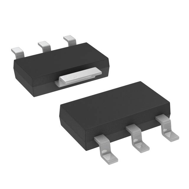
SOT−223
ST SUFFIX
CASE 318E
1
Input
2, 4 Ground
3
Output
74C−xxG
ALYWW
x
1
2
3
NC
V4274C−xx
AWLYYWWG
1
Input
2, 4 Ground
3
Output
AYW
74CxxG
G
1
xx
= 33 (3.3 V)
= 50 (5.0 V)
A
= Assembly Location
L, WL = Wafer Lot
Y, YY
= Year
W, WW = Work Week
G or G = Pb−Free Package
(Note: Microdot may be in either location)
ORDERING INFORMATION
See detailed ordering and shipping information on page 12 of
this data sheet.
© Semiconductor Components Industries, LLC, 2016
November, 2018 − Rev. 4
1
Publication Order Number:
NCV4274C/D
�NCV4274C
I
Q
Bandgap
Refernece
Current Limit and
Saturation Sense
−
+
Thermal
Shutdown
GND
Figure 1. Block Diagram
Pin Definitions and Functions
Pin No.
Symbol
1
I
2,4
GND
3
Q
Function
Input; Bypass directly at the IC with a ceramic capacitor to GND.
Ground
Output; Bypass with a capacitor to GND.
ABSOLUTE MAXIMUM RATINGS
Pin Symbol, Parameter
I, Input−to−Regulator
Symbol
Condition
Min
Max
Unit
V
Voltage
VI
−42
45
Current
II
Internally
Limited
Internally
Limited
I, Input peak Transient Voltage to Regulator with Respect
to GND (Note 1)
VI
60
V
Q, Regulated Output
Voltage
VQ
−1.0
40
V
Current
IQ
Internally
Limited
Internally
Limited
GND, Ground Current
IGND
−
100
mA
Junction Temperature
Storage Temperature
TJ
TStg
−40
−50
150
150
°C
°C
ESDHB
4
ESD Capability, Machine Model (Note 2)
ESDMM
200
V
ESD Capability, Charged Device Model (Note 2)
ESDCDM
1
kV
ESD Capability, Human Body Model (Note 2)
VQ = VI
kV
Stresses exceeding those listed in the Maximum Ratings table may damage the device. If any of these limits are exceeded, device functionality
should not be assumed, damage may occur and reliability may be affected.
1. Load Dump Test B (with centralized load dump suppression) according to ISO16750-2 standard. Guaranteed by design. Not tested in
production. Passed Class C.
2. This device series incorporates ESD protection and is tested by the following methods:
ESD HBM tested per AEC−Q100−002 (EIA/JESD22−A114)
ESD MM tested per AEC−Q100−003 (EIA/JESD22−A115)
Field Induced Charge Device Model ESD characterization is not performed on plastic molded packages with body sizes
很抱歉,暂时无法提供与“NCV4274CST33T3G”相匹配的价格&库存,您可以联系我们找货
免费人工找货- 国内价格
- 1+10.83240
- 10+9.12600
- 30+8.05680