NCV73830V1GEVB
NCV7383 FlexRay) Bus
Driver Evaluation Board
User's Manual
Introduction
http://onsemi.com
This document describes the NCV7383EVB Evaluation
board for the ON Semiconductor NCV7383 FlexRay Bus
Driver. The functionality and major parameters can be
evaluated with the NCV7383EVB board.
The NCV7383 is a single-channel FlexRay bus driver
compliant with the FlexRay Electrical Physical Layer
Specification Version 3.0.1, capable of communicating at
speeds of up to 10 Mb/s. It provides differential transmit and
receive capability between a wired FlexRay communication
medium on one side and a protocol controller and a host on
the other side.
NCV7383 mode control functionality is optimized for
nodes without the need of extended power management
provided by transceivers with permanent connection to the
car battery as is on NCV7381.
NCV7383 is primarily intended for nodes switched off by
ignition. Additional details can be found in the NCV7383
datasheet.
EVAL BOARD USER’S MANUAL
allows users immediately start with the NCV7383 FlexRay
Bus Driver. The MCU is preprogrammed with a firmware
which provides simple mode control and FlexRay
communication. With use of Freescalet BDM programmer
and a suitable development environment, the MCU
firmware can be freely modified and reprogrammed.
1
VIO
VCC
TxD
BP
TxEN
BM
RxD
GND
BGE
ERRN
STBN
CSN
SCK
SDO
Figure 2. NCV7383 Pin Connections
Board Hardware
The board consists of MCU with integrated 2-channel
FlexRay communication controller interconnected with two
separate FlexRay bus drivers (NCV7383), two voltage
regulators and peripherals. The board is prepared for various
modifications in power supply concept and FlexRay bus
termination, and allows simple extension of the system by
unused MCU pins. USB interface provides compatibility
with standard PC. The address of each board can be easily
modified by address switch what allows to create complex
FlexRay network without the need of reprogramming the
MCU. Implemented High Speed CAN interface can be used
as a diagnostic interface in a network built from several
nodes. For evaluation purposes NCV7383 is populated with
several LED diodes and most of the bus driver signals are
comfortable accessible to oscilloscope probes.
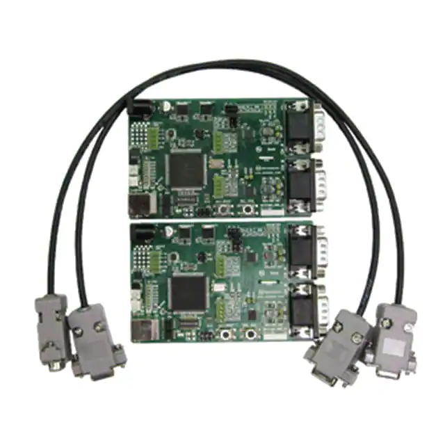
Figure 1. Evaluation Board Photo
The NCV7383EVB Evaluation board is a reference
design for stand-alone 2−channel FlexRay node. The board
is intended to give designers easy, quick and convenient
means for evaluation of NCV7383 FlexRay bus drivers. The
design incorporates complete node solution with possibility
of modifications and small board size. A set of two boards
© Semiconductor Components Industries, LLC, 2013
July, 2013 − Rev. 1
1
Publication Order Number:
EVBUM2172/D
�NCV73830V1GEVB
GENERAL FEATURES
• All NCV7383 digital I/O pins connected to test points –
FlexRay Transceiver
• Two separate FlexRay channels with NCV7383 Bus
•
•
•
easy connection to Logic Analyzer
Driver compliant with the FlexRay Electrical Physical
Layer Specification Version 3.0.1,
Reconfigurable bus termination – End node / Middle
node
Common mode Choke and additional ESD protection
footprint
SUBD-9 connectors – FlexRay bus
• 8 general purpose LEDs
• Address switch
• External Interrupt switch
Other
• Two Automotive Voltage regulators (Input battery
voltage up to 42 V)
• Power supplies voltage monitoring
• Instant 2-nodes FlexRay network with running
MCU
• Freescalet 16-bit MC9S12XF family MCU
• Integrated FlexRay Communication Controller
communication by connecting two NCV7383 EVBs.
• PC configuration software under development
(Protocol Specification Rev. 2.1)
(available upon request)
• Integrated CAN 2.0 A, B Controller
• Background Debug Module – single-wire
•
•
•
•
PCB Layout
• The FlexRay transceiver, the ESD protection and the
communication with host development system
512 k byte Flash
32 k byte RAM
50 MHz maximum CPU bus frequency
Relatively small 112-pin LQFP package
•
•
Peripherals
•
• Optical isolated USB interface (USB to UART
converter)
common mode choke are placed near to the FlexRay
the ECU connector
The FlexRay signal lines (BP, BM) are decoupled from
disturbances on the ECU board
The routing of the FlexRay lines (BP, BM, TxD and
TxEN) is symmetric
The distance between the lines BP and BM resp. TxD
and TxEN is minimized
• Additional CAN interface
GETTING STARTED
considered as Master Board. Node address is
configured by address switch SW12 – see Address
Switch for details.
4. Connect the boards according to Figure 3. Up to 5
boards with addresses 1 to 5 can be connected
together.
5. Connect the oscilloscope to any test-point as
needed.
6. When power supply is applied, MCU
automatically configures the FlexRay
Communication Controller setting based on the
current node address and initiates FlexRay
communication.
The NCV7383EVB board is fully assembled,
pre-programmed and can be immediately used for
evaluation. Only a few steps need be proceeded to get fully
working simple FlexRay network.
Connect the evaluation boards as follows:
1. Set the boards to default configuration according
to Jumpers and Default Configuration section.
2. Select one of the bus termination type (Bus
Termination Configuration section) and adapt the
respective devices. End node termination type is
recommended for 2-node network.
3. Set a different board address on each board. One
of the boards must be set with address 1 and is
http://onsemi.com
2
�NCV73830V1GEVB
Figure 3. Basic NCV7383 Evaluation Board connection
Power Modes
•
•
Normal Mode LED Signaling
The nodes can operate in two different power modes:
Normal mode – all the nodes continuously
communicates over the FlexRay bus.
Standby mode – the communication is suspended. Both
NCV7383 FlexRay transceivers are switched to Low
Power Standby operating mode. Indication LEDs are
switched off. The MCU is operating in low power
STOP mode where the oscillator is stopped and the
current consumption is substantially reduced.
The properly running setup should signal following
(Figure 4):
Enter Standby Mode Sequence
A transition to Standby mode can be initiated by the node
with address 1:
• Press and hold the Node1 #IRQ button for more than 3
seconds. The GO_TO_STANDBY signal is transmitted
over the FlexRay bus. All the nodes then synchronously
stop the communication and switch to Standby mode.
Figure 4. LEDs Signaling Description
• LED8 - LED4
•
Wakeup Sequence
The network operating in Standby mode can be woken-up
by any node:
• Press the #IRQ button on any node connected to the
network. The MCU is woken-up from STOP mode by
an external interrupt (#IRQ button pressed), resume
operation in Normal mode and automatically wake up
the rest of the network by the FlexRay Remote Wakeup
Pattern sent over the bus. Once all the nodes are
initialized, the FlexRay communication is restarted.
•
•
Toggling LED signals data was
received correctly in the particular slot (Slot 1 – Slot 5)
LED3 Each node transmits its own #IRQ Button
status (BTN_IRQ_DOWN signal). This LED signals
that one of the nodes in the network detected the #IRQ
button pressed.
LED2 When the #IRQ button is pressed and held
down, the LED2 is gradually decreasing intensity
indicating the time remaining to ENTER STANDBY
MODE event (100% to 0% in 2.4 seconds).
LED1 LED1 changes intensity according to input
battery voltage.
⋅ The LED intensity is directly proportional to the
battery voltage in range of 10 V to 14V.
http://onsemi.com
3
�NCV73830V1GEVB
⋅ Battery voltage being below 10 V is indicated by
LED1 OFF state.
⋅ Battery voltage exceeding 14 V is indicated by
LED1 full intensity (Figure 5).
Standby Mode LED Signaling
In Standby mode, all the LEDs except LED8 are switched
OFF. The LED8 is turned ON with very low intensity,
signaling the MCU is correctly operating in the low power
STOP mode and is ready to be woken-up.
LED1 Intensity [%]
FlexRay Communication Cycle Configuration
100%
Cycle Length: 10000 us
Number of Static Slots: 10 (5 slots active)
Static Slot Length: 31 us
Static Slot Payload Length: 6 Words
Dynamic Segment: Not used
Symbol Window Length: 14 us
0%
10 V
FB20120813.01
VBAT [V]
14 V
Figure 5. LED1 Intensity vs. Battery Voltage
SLOT
1
2
3
4
5
Node 1
Tx
Rx
Rx
Rx
Rx
Node 2
Rx
Tx
Rx
Rx
Rx
Node 3
Rx
Rx
Tx
Rx
Rx
Node 4
Rx
Rx
Rx
Tx
Rx
Node 5
Rx
Rx
Rx
Rx
Tx
Each node is assigned to one communication slot. The
Slot number corresponds to particular Node address.
6
7
8
9
10
Static Segment
Symbol
Window
310 ms
14 ms
NIT
9676 ms
Figure 6. FlexRay Communication Cycle Configuration (Tx − Transmitter Buffer, Rx − Receive Buffer)
http://onsemi.com
4
�NCV73830V1GEVB
BOARD OVERVIEW
Basic Interface
Figure 7. NCV7383EVB Connectors and Switches
Legend:
9. BDM Connector (MCU debugging interface)
10. Power supply input connector
11. Aux digital I/O connector
12. CAN backbone connector 1
13. CAN backbone connector 2
14. USB interface
15. MCU Interrupt Request connector
16. Address switch
17. FlexRay CC Strobe output signals
1. Power supply input connector
2. Aux digital I/O connector
3. CAN backbone connector 1
4. CAN backbone connector 2
5. USB interface
6. MCU Interrupt Request connector
7. Address switch
8. FlexRay CC Strobe output signals
Power Supply Input Connector
signals can be also used as general Input / Output signals for
debugging or other purposes.
Power supply input socket. Plug diameter 2.1 mm, length
14 mm. Maximum input voltage 42 V (Limited by onboard
voltage regulators input voltage range).
Figure 8. Power Supply Input Connector
Figure 9. Aux Digital I/O Connector
Aux Digital I/O Connector
CAN Backbone Connectors
These pin header contains 8 auxiliary MCU signals – one
complete SPI interface (4 pins), one UART interface (2 pins)
and 2 signals connected to MCU ADC interface. These
CAN backbone network is created as parallel connection
of several boards. Each board contains two equivalent
http://onsemi.com
5
�NCV73830V1GEVB
FlexRay BD Digital Signals Test Points Headers
connectors in parallel, so whole network can be prepared
using only simple point-to-point twisted pair.
PCB1
PCB2
These headers are intended to be used as a test points for
digital probes. Headers contain all FlexRay BD digital input
and output signals.
Test points for both FlexRay channel A and channel B are
placed on separated headers (J73 – channel A, J83 –
channel B).
PCB3
Figure 10. CAN Backbone Connectors
USB Interface
Standard B type USB socket is used for connection to PC.
USB interface is bus powered and electrically isolated from
the rest of the board, so it is not possible to supply this board
via USB.
Figure 13. FlaxRay BD Digital Signals Test Points
FlexRay BD Analog Signals Test Points
FlexRay CC Strobe Output Signals
The MCU FlexRay block provides a number of strobe
signals for observing internal protocol timing related signals
in the protocol engine.
STB1
STB3
STB0
STB2
•
•
•
•
•
•
Figure 11. FlexRay CC Strobe Output Signals
There are 6 analog test points on the board:
BP – FlexRay Bus Plus terminal (Channel A)
BM – FlexRay Bus Minus terminal (Channel A)
VIO – Bus Driver VIO Power Supply input
BP – FlexRay Bus Plus terminal (Channel B)
BM – FlexRay Bus Minus terminal (Channel B)
VCC – Bus Driver VCC Power Supply input
FlexRay Bus Connectors
FlexRay EPL Specification [2] does not prescribe certain
connectors for FlexRay systems. Common used 9-pin
D-Sub connectors were chosen as a suitable connector,
whose electrical characteristics satisfy the specification.
BDM Connector (MCU Debugging Interface)
The BDM module provides a single-wire communication
with host development system (Programming and
debugging interface).
BKGD
GND
NC
RESET
NC
VCC
Figure 12. BDM Connector
Table 1. FLEXRAY CONNECTOR
Pin #
Signal
Description
Connection
1
-
Reserved
Not Connected
2
FR_BM
BM bus line
BM
3
FR_GND
Ground
GND
4
-
Reserved
Not Connected
5
-
Reserved
Not Connected
6
-
Reserved
Not Connected
7
FR_BP
BP bus line
BP
8
-
Reserved
Not Connected
9
(FR_Vbat)
Optional FR external supply
Main supply line
NOTE: Connector Type: 9−pin D−sub (DIN 41652 or corresponding international standard), plug (male)
http://onsemi.com
6
ESD Protection
Yes (Optional)
Yes (Optional)
Yes
�NCV73830V1GEVB
Jumpers and Default Configuration
Figure 14. Jumpers and Soldering Straps
Table 2. 2−PIN JUMPER
Table 3. 3−PIN JUMPER
Open
1 2 3
Open
Closed
Closed position 1−2
Closed position 2−3
http://onsemi.com
7
�NCV73830V1GEVB
Table 4. NCV7383 EVB JUMPERS CONFIGURATION
Jumper
J3
Function
Bus Driver VIO supply
Configuration
Open
Closed
J4
Bus Driver VCC supply
Bus Driver VIO connected to voltage regulator output
Open
Bus Driver VCC unsupplied
Closed
J40
CAN bus termination
J52
General purpose LED
Bus Driver VCC connected to voltage regulator output
Open
CAN bus without termination
Closed
J53
UART power supply
J54
MCU output mcu_PP0 function
J87
Channel B SCK pin connection
J89
J75
J85
Channel B SDO pin connection
Channel A Bus Driver digital
input pull-ups
Channel B Bus Driver digital
input pull-ups
Description
Bus Driver VIO unsupplied
LEDs Disabled
Closed
LEDs Enabled
Open
UART Disabled
Closed
UART Enabled
Open
LED D101 not used
Closed
SCK_B disconnected
Closed 1-2
SCK_B connected to common hardware SPI interface
Closed 2-3
SCK_B connected to separated software SPI interface
Open
SDO_B disconnected
Closed 1-2
SDO_B connected to common hardware SPI interface
Closed 2-3
SDO_B connected to separated software SPI interface
Open
TxEN, SCN and SCK pull-ups disconnected from VIO
Closed
Closed
5V – 5V_BD
Closed
Closed
Open
Closed
LED D101 connected to PWM0 output
Open
Open
Closed
3V3 – 3V3_BD
CAN bus with 120 W termination
Open
Closed
Default
Closed 1-2
Closed 1-2
Closed
TxEN, SCN and SCK pull-ups connected to VIO
TxEN, SCN and SCK pull-ups disconnected from VIO
Closed
TxEN, SCN and SCK pull-ups connected to VIO
Bus Termination Configuration
Figure 15. FlexRay Bus Termination Assembly Drawing (R72, R82, C77, C87 placed on the BOTTOM side)
http://onsemi.com
8
�NCV73830V1GEVB
BP
FlexRay Bus
Driver
BUS
BM
C75
C85
C76
C86
R70
R80
R71
R81
R72
R82
C77
C87
Figure 16. FlexRay Bus Termination Connection (Channel A: R7x, C7x; Channel B: R8x, C8x)
Table 5. FLEXRAY BUS TERMINATION CONFIGURATION AND PARAMETERS
End node
Middle node – Variant 1
Middle node – Variant 2
Component
(Low-Ohmic termination)
(High-Ohmic termination)
(Custom termination)
Ch. A: C75, C76
Ch. B: C85, C86
Short
Short
100 pF
Ch. A: R70, R71
Ch. B: R80, R81
47 W
1300 W
24 W
Ch. A: R72
Ch. B: R82
Not Assembled
Not Assembled
47 W
Ch. A: C77
Ch. B: C87
4.7 nF
4.7 nF
4.7 pF
Switches and Pushbuttons
Figure 17. Switches Description
• SW10...MCU Reset button
• SW11...MCU External interrupt button
• SW12...8-way DIP switch. The function depends on the
MCU program. As default it is used for setting a node
address.
http://onsemi.com
9
�NCV73830V1GEVB
⋅ The switch configuration shown in this figure
means binary 0b00000010 (Node address is set
to 2).
Address Switch
This switch is used for setting a node number. Each board
is programmed with the same firmware, so every node in the
network must be configured with different unique number.
Be careful:
MCU Reset Button
This button is connected directly to MCU RESET pin.
0123456 7
MCU External Interrupt Button
The MCU interrupt module support one maskable
interrupt input. This input is connected to SW11.
LEDs
Figure 18. Address Switch
Three power LEDs indicate proper function of voltage
regulators. In case the MCU and the NCV7381 bus drivers
IO cells use the same power supply (as by default) MCU
VCC LED and BD VIO LED signalling is also the same.
The board contains a bank of eight general purpose LEDs
(Green). Their function depends on the MCU program.
There is also USB indication LED which is used to signal
ongoing USB data transmission.
⋅ LSB is situated on the left.
⋅ ON means the particular switch is closed and
output is Logical 0!
⋅ OFF means the particular switch is open and
output is Logical 1!
Figure 19. LEDs Description
http://onsemi.com
10
�NCV73830V1GEVB
BLOCK DIAGRAM
PROGRAMMING/
DEBUG INTERFACE
CAN
BACKBONE
USB
INTERFACE
SWITCHES
CLOCK
LED’s
MCU
EXTERNAL
RESET
MC9S12XF512MLM
POWER SUPPLIES
FlexRay CC A
AUX I/O PINS
FlexRay CC
AUX OUTPUTS
FlexRay CC B
MCU & FR BD IO
VIO 3V3
FR BD VCC
VCC 5V
NCV7383
FlexRay BD A
NCV7383
FlexRay BD B
PASSIVE NETWORK
PASSIVE NETWORK
FlexRay CONNECTOR
FlexRay CONNECTOR
Figure 20. NCV7383 Evaluation Board Block Diagram
NCV7383 TYPICAL APPLICATION DIAGRAM
IN
VIO
reg.
VCC
reg.
OUT
OUT
CVIO
VIO
FlexRay
Communication
Controller
TxD
TxEN
RxD
Bus Guardian
BGE
Host Interface
STBN
ERRN
SPI
CVCC
VCC
NCV7383
CMC
BP
BP
BM
BM
CSN
SCK
SDO
RBUS1
MCU
VBAT
IN
GND
RBUS2
ECU
CBUS
FB20110411.12
Figure 21. NCV7383 FlexRay Bus Driver Typical Application Diagram
http://onsemi.com
11
GND
�NCV73830V1GEVB
Table 6. RECOMMENDED EXTERNAL COMPONENTS FOR THE APPLICATION DIAGRAM
Component
Function
Min.
Typ.
Max.
Unit
Note
CVCC
Decoupling capacitor on VCC supply line, ceramic
100
nF
CVIO
Decoupling capacitor on VIO supply line, ceramic
100
nF
RBUS1
Bus termination resistor
47.5
W
(1)
RBUS2
Bus termination resistor
47.5
W
(1)
CBUS
Common-mode stabilizing capacitor, ceramic
4.7
nF
(2)
CMC
Common-mode choke
100
mH
1. Tolerance ±1%, type 0805. The value RBUS1 + RBUS2 should match the nominal cable impedance.
2. Tolerance ±20%, type 0805.
SPECIFICATIONS
Power Supply
The Evaluation board can be powered either via DC
power supply input socket with plug diameter 2.1 mm and
length 14 mm or by one of the FlexRay bus connectors (See
the connector description Table 1). Maximum input voltage
(42 V) is limited by on-board voltage regulators input
voltage range.
Split Termination
In order to achieve a better EMC performance, it is
recommended to make use of a so-called split termination in
all ECUs, where the Termination resistance RT is split into
two equal parts RTA and RTB [2].
Figure 22. ECU with Split Termination [2]
The serial RC combination (R1; C1) at the centre tap of the
split termination provides a termination to GND for
common mode signals. R1 is preferably omitted. Typical
values are given in the following table:
Table 7. TERMINATION PARAMETERS
Typ
Units
R1
Name
Resistor
Description
< 10
W
C1
Capacitor
4700
pF
2 × |RTA - RTB| / (RTA + RTB)
Matching of termination resistors
≤2
%
For RTA and RTB the use of 1% tolerated resistors leads to
a matching of 2%.
The better the matching of the split termination resistors
RTA and RTB, the lower the electromagnetic emission.
BP
FlexRay Bus
Driver
Standard Termination
BUS
BM
RTA
Recommended bus split termination is shown in the
Figure 23. Considering passive network, without active
stars, proper termination should be applied at the two nodes
that have the maximum electrical distance on the bus. The
sum of termination resistors values should match the
nominal cable impedance. At other nodes a high-ohmic split
termination should be applied.
RTB
C1
Figure 23. Basic Split Termination
http://onsemi.com
12
�NCV73830V1GEVB
Table 8. BASIC SPLIT TERMINATION PARAMETERS
Value
Name
Description
RTA, RTB
Termination resistors
C1
Capacitor
End node
Middle node
Units
47
1300
W
4700
4700
pF
Custom Termination
BP
In some cases a specific termination topology is required
for middle modes. Such a termination connection and
typical values are shown in Figure 25 and Table 9.
FlexRay Bus
Driver
BUS
BM
CMC
BP
FlexRay Bus
Driver
BUS
BM
RTA
CTA
CTB
RTA
RTB
RTB
R1
C1
C1
Figure 25. Middle Node Split Termination
Figure 24. End Node Split Termination
Table 9. CUSTOM SPLIT TERMINATION PARAMETERS
Value
Name
Description
End node
Middle node
Units
47
24
W
4700
4.7
pF
RTA, RTB
Termination resistors
C1
Capacitor
R1
Resistor
−
47
W
CTA, CTB
Termination capacitors
−
100
pF
Common Mode Choke
choke represents high impedance for common mode signals.
The parasitic stray inductance should be as low as possible
in order to keep oscillations on the bus low. The common
mode choke is placed between transceiver and split
termination [2].
A common mode choke is used to improve the emission
and immunity performance. The function of the common
mode choke is to force the current in both signal wires to be
of the same strength, but opposite direction. Therefore, the
Figure 26. ECU with Split Termination and Common Mode Choke [2]
http://onsemi.com
13
�NCV73830V1GEVB
Table 10. COMMON−MODE CHOKE REQUIREMENTS [2]
Name
Description
Typ
Units
≤1
W
Main inductance
≥ 100
mH
Stray inductance


 工商网监
湘ICP备2023018690号
工商网监
湘ICP备2023018690号
