NCV8508 5.0 V, 250 mA LDO with Watchdog and RESET
The NCV8508 is a precision micropower Low Dropout (LDO) voltage regulator. The part contains many of the required operational requirements for powering microprocessors. Its robustness makes it suitable for severe automotive environments. In addition to being a good fit for the automotive environment, the NCV8508 is ideal for use in battery operated, microprocessor controlled equipment because of its extremely low quiescent current.
16
http://onsemi.com MARKING DIAGRAMS
16 NCV85085 AWLYYWW
Features
• • • • •
• •
• • •
Output Voltage: 5.0 V ±3.0% Output Voltage IOUT Up to 250 mA Quiescent Current Independent of Load Micropower Compatible Control Functions: ♦ Wakeup ♦ Watchdog ♦ RESET Low Quiescent Current (100 mA typ) Protection Features: ♦ Thermal Shutdown ♦ Short Circuit ♦ 45 V Operation Internally Fused Leads in SO−16L Package NCV Prefix for Automotive and Other Applications Requiring Site and Control Changes Pb−Free Package is Available*
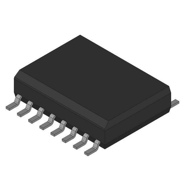
1 SO−16L DW SUFFIX CASE 751G
1
NCV85085 AWLYYWW D2PAK−7 DPS SUFFIX CASE 936AB 1
A WL YY WW
= Assembly Location = Wafer Lot = Year = Work Week
PIN CONNECTIONS
SO−16L 1 NC NC NC GND GND NC Sense VOUT 16 Delay RESET Wakeup GND GND WDI NC VIN Tab = GND Lead 1. VOUT 2. VIN 3. WDI 4. GND 5. Wakeup 6. RESET 7. Delay 1
D2PAK−7
*For additional information on our Pb−Free strategy and soldering details, please download the ON Semiconductor Soldering and Mounting Techniques Reference Manual, SOLDERRM/D.
ORDERING INFORMATION
See detailed ordering and shipping information in the package dimensions section on page 10 of this data sheet.
© Semiconductor Components Industries, LLC, 2004
1
August, 2004 − Rev. 20
Publication Order Number: NCV8508/D
�NCV8508
MRA4004T3 VBAT C1* 0.1 mF VIN VOUT C2 1.0 mF WDI VDD I/O RESET
NCV8508
Delay RESET WAKEUP
GND RDelay 60 k
I/O
*C1 required if regulator is located far from power supply filter. *
Microprocessor
.
Figure 1. Application Circuit
MAXIMUM RATINGS
Rating Input Voltage, VIN Output Voltage, VOUT ESD Susceptibility: Human Body Model Machine Model Logic Inputs/Outputs (RESET, WDI, Wakeup) Operating Junction Temperature, TJ Storage Temperature Range, TS Package Thermal Resistance, SO−16L: Junction−to−Case, RqJC Junction−to−Ambient, RqJA Package Thermal Resistance, D2PAK, 7−Lead: Junction−to−Case, RqJC Junction−to−Ambient, RqJA Lead Temperature Soldering: Reflow: (SMD styles only) (Note 1) 4.0 10 to 50 (Note 2) 240 peak (Note 3) 18 80 2.0 200 −0.3 to +7.0 −40 to150 −55 to +150 kV V V °C °C °C/W °C/W °C/W °C/W °C Value −0.3 to 45 −0.3 to 18 Unit V V
Maximum ratings are those values beyond which device damage can occur. Maximum ratings applied to the device are individual stress limit values (not normal operating conditions) and are not valid simultaneously. If these limits are exceeded, device functional operation is not implied, damage may occur and reliability may be affected. 1. 60 second maximum above 183°C. 2. Depending on thermal properties of substrate RqJA = RqJC + RqJCA. 3. −5°C/+0°C allowable conditions.
http://onsemi.com
2
�NCV8508
ELECTRICAL CHARACTERISTICS (−40°C ≤ TJ ≤ 125°C; 6.0 V ≤ VIN ≤ 28 V, 100 mA ≤ IOUT ≤ 150 mA, C2 = 1.0 mF, RDelay = 60 k;
unless otherwise specified.) Characteristic OUTPUT Output Voltage Dropout Voltage (VIN − VOUT) Load Regulation Line Regulation Current Limit Thermal Shutdown Quiescent Current RESET Threshold Output Low Output High Delay Time − RLOAD = 10 k to VOUT, VOUT ≥ 1.0 V RLOAD = 5.1 k to VOUT, VOUT ≥ 1.0 V RLOAD = 10 k to GND RLOAD = 5.1 k to GND VIN = 14 V, RDelay = 60 k, IOUT = 5.0 mA VIN = 14 V, RDelay = 120 k, IOUT = 5.0 mA 4.50 − VOUT − 0.5 VOUT − 1.0 2.0 − 4.65 0.2 0.4 VOUT − 0.25 VOUT − 0.5 3.0 6.0 4.80 0.4 0.8 − 4.0 − V V V ms ms − IOUT = 150 mA. Note 4 VIN = 14 V, 100 mA ≤ IOUT ≤ 150 mA 6.0 V ≤ VIN ≤ 28 V, IOUT = 5.0 mA − Guaranteed by Design VIN = 12 V, IOUT = 150 mA, (see Figure 6) 4.85 − − − 250 150 − 5.00 450 5.0 5.0 400 180 100 5.15 900 30 50 − 210 150 V mV mV mV mA °C mA Test Conditions Min Typ Max Unit
WATCHDOG INPUT Threshold High Threshold Low Hysteresis Input Current Pulse Width WDI = 6.0 V 50% WDI falling edge to 50% WDI rising edge and 50% WDI rising edge to 50% WDI falling edge, (see Figure 5) − − − 70 − − − 5.0 − − 100 0.1 − − 30 − +10 − %VOUT %VOUT mV mA ms
WAKEUP OUTPUT (VIN = 14 V, IOUT = 5.0 mA) Wakeup Period Wakeup Duty Cycle Nominal RESET HIGH to Wakeup Rising Delay Time See Figures 4 and 5, RDELAY = 60 k See Figures 4 and 5, RDELAY = 120 k See Figure 3 RDELAY = 60 k 50% RESET rising edge to 50% Wakeup edge, RDELAY = 120 k (see Figures 3 and 4) 50% WDI falling edge to 50% Wakeup falling edge 50% RESET falling edge to 50% Wakeup falling edge. VOUT = 5.0 V→ 4.5 V RLOAD = 10 k to VOUT, VOUT ≥ 1.0 V RLOAD = 5.1 k to VOUT, VOUT ≥ 1.0 V RLOAD = 10 k to GND RLOAD = 5.1 k to GND 18 − 45 9.0 − 25 50 50 12.5 25 32 − 55 16 − ms ms % ms ms
Wakeup Response to Watchdog Input Wakeup Response to RESET
− −
0.1 0.1
5.0 5.0
ms ms
Output Low Output High DELAY Output Voltage
− VOUT − 0.5 VOUT − 1.0
0.2 0.4 VOUT − 0.25 VOUT − 0.5
0.4 0.8 −
V V
IDELAY = 50 mA. Note 5
−
1.25
−
V
4. Measured when the output voltage has dropped 100 mV from the nominal value. (see Figure 12) 5. Current drain on the Delay pin directly affects the Delay Time, Wakeup Period, and the RESET to Wakeup Delay Time.
http://onsemi.com
3
�NCV8508
PACKAGE PIN DESCRIPTION
PACKAGE PIN # D2PAK−7 1 2 3 4 5 6 SO−16L 8 9 11 4, 5, 12, 13 14 15 PIN SYMBOL VOUT VIN WDI GND Wakeup RESET FUNCTION Regulated output voltage ± 3.0%. Supply Voltage to the IC. CMOS compatible input lead. The Watchdog function monitors the falling edge of the incoming signal. Ground connection. CMOS compatible output consisting of a continuously generated signal used to “wake up” the microprocessor from sleep mode. CMOS compatible output lead RESET goes low whenever VOUT drops by more than 7.0% from nominal, or during the absence of a correct Watchdog signal. Buffered bandgap voltage used to create timing current for RESET and Wakeup from RDelay. No Connection. Kelvin connection which allows remote sensing of the output voltage for improved regulation. Connect to VOUT if remote sensing is not required.
7 − −
16 1−3, 6, 10 7
Delay NC Sense
VIN
− +
Charge Pump 11 V 1.25 V
+ −
Internally connected on 7 lead D2PAK Current Limit Thermal Shutdown
VOUT Sense
Bandgap Reference
RESET
+
WDI Falling Edge Detect Timing Circuit
Delay
−
Watchdog Circuit
Wakeup Circuit
Wakeup
Figure 2. Block Diagram
http://onsemi.com
4
�NCV8508
TIMING DIAGRAMS
VIN
RESET
Wakeup Duty Cycle = 50%
Wakeup
WDI
VOUT POR RESET High to Wakeup Delay Time Power Up Microprocessor Sleep Mode
WDI Pulse Must Occur with Wakeup in Low State for 50% Duty Cycle. Reference Figure 17 for Occurrence of WDI with Wakeup in High State.
Normal Operation with Varying Watchdog Signal
Figure 3. Power Up, Sleep Mode and Normal Operation
VIN RESET Wakeup WDI
RESET Delay Time
VOUT POR RESET High to Wakeup Delay Time Wakeup Period RESET High to Wakeup Delay Time
Figure 4. Error Condition: Watchdog Remains Low and a RESET Is Issued
RESET Wakeup
Wakeup Period
WDI RESET Threshold VOUT Watchdog Pulse Width POR Watchdog Pulse Width Power Down POR
Figure 5. Power Down and Restart Sequence
http://onsemi.com
5
�NCV8508
TYPICAL PERFORMANCE CHARACTERISTICS
120 −40°C −600 VOUT Transient, mV −500 −400 −300 −200 −100 200 250 0 0 50 10 mF ESR = 3.4 W 100 mF ESR = 1.3 W 100 150 Switching Current, mA 200 250 1.0 mF ESR = 4.6 W −700
110 IQ, mA +25°C
100
+125°C 90 0 50 100 150 IOUT, mA
Figure 6. Quiescent Current vs Output Current
Figure 7. Load Transient Response
3.7 3.6 3.5 POR Delay, ms POR Delay, ms 3.4 3.3 3.2 3.1 3.0 2.9 2.8 2.7 −40 −20 0 20 40 60 80 Temperature, °C 100 120 140
14 12 10 8 6 4 2 0 15 60 105 150 RDELAY, kW 195 240
Figure 8. POR Delay vs Temp, RDELAY = 60 kW
Figure 9. POR Delay vs RDELAY
27.0 26.5 Wakeup Period, ms 26.0 25.5 25.0 24.5 24.0 23.5 23.0 −40 −20 0 20 40 60 80 Temperature (°C) 100 120 140
100 90 80 70 RDELAY, ms 60 50 40 30 20 10 0 15 60 105 150 RDELAY, kW 195 240
Figure 10. Wakeup Period vs Temp, RDELAY = 60 kW
Figure 11. Wakeup Period vs RDELAY
http://onsemi.com
6
�NCV8508
TYPICAL PERFORMANCE CHARACTERISTICS
1.0 0.9 0.8 Dropout Voltage (V) 0.7 0.6 0.5 0.4 0.3 0.2 0.1 0.0 0 25 50 75 100 125 150 175 200 225 250 Output Current (mA) −40°C +25°C +125°C Output Voltage (V)
5.10
5.05
5.00 VIN = 14 V IOUT = 5.0 mA 4.95
4.90 −40 −25 −10
5
20 35 50 65 Temperature (°C)
80
95 110 125
Figure 12. Dropout Voltage vs Output Current
Figure 13. Output Voltage vs Temperature
160 140 120
1000
Unstable Region 100 ESR (W)
IOUT (mA)
100 80 60 40 20 0 1.0 1.5 2.0 2.5 3.0 3.5 4.0 VIN (V) RL = 33 W
Stable Region 10
4.5
5.0
5.5
6.0
1 0 5 10 15 20 25
C = 1.0 mF, 10 mF 30 35 40 45 Output Current (mA)
Figure 14. Output Current vs Input Voltage
Figure 15. Output Capacitor ESR
DEFINITION OF TERMS Dropout Voltage: The input−output voltage differential at which the circuit ceases to regulate against further reduction in input voltage. Measured when the output voltage has dropped 100 mV from the nominal value obtained at 14 V input, dropout voltage is dependent upon load current and junction temperature. Input Voltage: The DC voltage applied to the input terminals with respect to ground. Line Regulation: The change in output voltage for a change in the input voltage. The measurement is made under conditions of low dissipation or by using pulse techniques such that the average chip temperature is not significantly affected. Load Regulation: The change in output voltage for a change in load current at constant chip temperature. Quiescent Current: The part of the positive input current that does not contribute to the positive load current. The regulator ground lead current. Ripple Rejection: The ratio of the peak−to−peak input ripple voltage to the peak−to−peak output ripple voltage. Current Limit: Peak current that can be delivered to the output.
http://onsemi.com
7
�NCV8508
DETAILED OPERATING DESCRIPTION The NCV8508 is a precision micropower voltage regulator with very low quiescent current (100 mA typical at 250 mA load). A typical dropout voltage is 450 mV at 150 mA. Microprocessor control logic includes Watchdog, Wakeup and RESET. This unique combination of extremely low quiescent current and full microprocessor control makes the NCV8508 ideal for use in battery operated, microprocessor controlled equipment in addition to being a good fit in the automotive environment. The NCV8508 Wakeup function brings the microprocessor out of Sleep mode. The microprocessor in turn, signals its Wakeup status back to the NCV8508 by issuing a Watchdog signal. The Watchdog logic function monitors an input signal (WDI) from the microprocessor. The NCV8508 responds to the falling edge of the Watchdog signal which it expects at least once during each Wakeup period. When the correct Watchdog signal is received, a falling edge is issued on the Wakeup signal line. RESET is independent of VIN and operates correctly to an output voltage as low as 1.0 V. A signal is issued in any of three situations. During power up the RESET is held low until the output voltage is in regulation. During operation if the output voltage shifts below the regulation limits, the RESET toggles low and remains low until proper output voltage regulation is restored. And finally, a RESET signal is issued if the regulator does not receive a Watchdog signal within the Wakeup period. The RESET pulse width, Wakeup signal frequency, and Wakeup delay time are all set by one external resistor, RDelay. The Delay pin is a buffered bandgap voltage (1.25 V). It can be used as a reference for an external tracking regulator as shown in Figure 16. The regulator is protected against short circuit and thermal runaway conditions. The device runs through 45 volt transients, making it suitable for use in automotive environments.
MRA4004T3 VIN VBAT 0.1 mF 1.0 mF VIN VOUT
200 mA
5V 10 mF
12 k
NCV8508
Delay GND 60 k 0.1 mF
CS8182
VREF/ENABLE GND
Adj 3.9 k
Figure 16. Application Circuit
http://onsemi.com
8
�NCV8508
CIRCUIT DESCRIPTION
Functional Description
To reduce the drain on the battery a system can go into a low current consumption mode when ever its not performing a main routine. The Wakeup signal is generated continuously and is used to interrupt a microcontroller that is in sleep mode. The nominal output is a 5.0 volt square wave (voltage generated from VOUT) with a duty cycle of 50% at a frequency that is determined by a timing resistor, RDelay. When the microprocessor receives a rising edge from the Wakeup output, it must issue a Watchdog pulse and check its inputs to decide if it should resume normal operations or remain in the sleep mode. The first falling edge of the Watchdog signal causes the Wakeup to go low within 2.0 ms (typ) and remain low until the next Wakeup cycle (see Figure 17). Other Watchdog pulses received within the same cycle are ignored (Figure 3). During power up, RESET is held low until the output voltage is in regulation. During operation, if the output voltage shifts below the regulation limits, the RESET toggles low and remains low until proper output voltage regulation is restored. After the RESET delay, RESET returns high. The Watchdog circuitry continuously monitors the input Watchdog signal (WDI) from the microprocessor. The absence of a falling edge on the Watchdog input during one Wakeup cycle will cause a RESET pulse to occur at the end of the Wakeup cycle. (see Figure 4). The Wakeup output is pulled low during a RESET regardless of the cause of the RESET. After the RESET returns high, the Wakeup cycle begins again (see Figure 4). The RESET Delay Time, Wakeup signal frequency and RESET high to Wakeup delay time are all set by one external resistor RDelay. Wakeup Period = (4.17 × 10⁻⁷)RDelay RESET Delay Time = (5.21 × 10⁻⁸)RDelay RESET HIGH to Wakeup Delay Time = (2.08 × 10⁻⁷)RDelay
Resistor temperature coefficient and tolerance as well as the tolerance of the NCV8508 must be taken into account in order to get the correct system tolerance for each parameter.
WDI
Wakeup
Wakeup Response to WDI
Figure 17. Wakeup Response to WDI
RESET
Wakeup
Wakeup Response to RESET
Figure 18. Wakeup Response to RESET (Low Voltage)
http://onsemi.com
9
�NCV8508
APPLICATION NOTES
Thermal Resistance, Junction to Ambient, RqJA, (°C/W)
Calculating Power Dissipation in a Single Output Linear Regulator
100 90 80 70 60 50 40 0 0.5 1.0 1.5 2.0 Copper Area (inch2) 2.5 3.0
The maximum power dissipation for a single output regulator (Figure 19) is:
PD(max) + [VIN(max) * VOUT(min)] IOUT(max) ) VIN(max)IQ
(1)
where: VIN(max) is the maximum input voltage, VOUT(min) is the minimum output voltage, IOUT(max) is the maximum output current for the application, and IQ is the quiescent current the regulator consumes at IOUT(max).
IIN VIN IOUT SMART REGULATOR® VOUT
Figure 20. 16 Lead SOW (4 Leads Fused), qJA as a Function of the Pad Copper Area (2 oz. Cu Thickness), Board Material = 0.0625, G−10/R−4
} Control Features
IQ
Heatsinks
Figure 19. Single Output Regulator with Key Performance Parameters Labeled
Once the value of PD(max) is known, the maximum permissible value of RqJA can be calculated:
T RqJA + 150°C * A PD
(2)
A heatsink effectively increases the surface area of the package to improve the flow of heat away from the IC and into the surrounding air. Each material in the heat flow path between the IC and the outside environment will have a thermal resistance. Like series electrical resistances, these resistances are summed to determine the value of RqJA:
RqJA + RqJC ) RqCS ) RqSA
(3)
The value of RqJA can then be compared with those in the package section of the data sheet. Those packages with RqJA’s less than the calculated value in Equation 2 will keep the die temperature below 150°C. In some cases, none of the packages will be sufficient to dissipate the heat generated by the IC, and an external heatsink will be required.
ORDERING INFORMATION
Device NCV8508DW50 NCV8508DW50G NCV8508DW50R2 NCV8508D2T50 NCV8508D2T50G NCV8508D2T50R4 Output Voltage 5.0 V 5.0 V 5.0 V 5.0 V 5.0 V 5.0 V
where: RqJC = the junction−to−case thermal resistance, RqCS = the case−to−heatsink thermal resistance, and RqSA = the heatsink−to−ambient thermal resistance. RqJC appears in the package section of the data sheet. Like RqJA, it too is a function of package type. RqCS and RqSA are functions of the package type, heatsink and the interface between them. These values appear in heatsink data sheets of heatsink manufacturers.
Package SO−16L SO−16L (Pb−Free) SO−16L D2PAK−7 D2PAK−7 (Pb−Free) D2PAK−7
Shipping† 47 Units / Rail 47 Units / Rail 1000 / Tape & Reel 50 Units / Rail 50 Units / Rail 750 / Tape & Reel
†For information on tape and reel specifications, including part orientation and tape sizes, please refer to our Tape and Reel Packaging Specifications Brochure, BRD8011/D.
http://onsemi.com
10
�NCV8508
PACKAGE DIMENSIONS
SO−16L DW SUFFIX CASE 751G−03 ISSUE C
D
16 M 9
A
q
h X 45 _
M
8X
0.25
E
NOTES: 1. DIMENSIONS ARE IN MILLIMETERS. 2. INTERPRET DIMENSIONS AND TOLERANCES PER ASME Y14.5M, 1994. 3. DIMENSIONS D AND E DO NOT INLCUDE MOLD PROTRUSION. 4. MAXIMUM MOLD PROTRUSION 0.15 PER SIDE. 5. DIMENSION B DOES NOT INCLUDE DAMBAR PROTRUSION. ALLOWABLE DAMBAR PROTRUSION SHALL BE 0.13 TOTAL IN EXCESS OF THE B DIMENSION AT MAXIMUM MATERIAL CONDITION. MILLIMETERS DIM MIN MAX A 2.35 2.65 A1 0.10 0.25 B 0.35 0.49 C 0.23 0.32 D 10.15 10.45 E 7.40 7.60 e 1.27 BSC H 10.05 10.55 h 0.25 0.75 L 0.50 0.90 q 0_ 7_
H
B
1
8
16X
B TA
S
B B
S
0.25
M
A
A1
14X
e
SEATING PLANE
T
C
http://onsemi.com
11
L
�NCV8508
PACKAGE DIMENSIONS
D2PAK−7 (SHORT LEAD) DP SUFFIX CASE 936AB−01 ISSUE O
NOTES: 1. DIMENSIONS AND TOLERANCING PER ANSI Y14.5M, 1982. 2. CONTROLLING DIMENSION: INCH.
K
A E
TERMINAL 8
U
DIM A B C D E G H K L M N P R S U V
S B H L P G N R M
V
D
INCHES MIN MAX 0.396 0.406 0.326 0.336 0.170 0.180 0.026 0.036 0.045 0.055 0.050 REF 0.539 0.579 0.055 0.066 0.000 0.010 0.100 0.110 0.017 0.023 0.058 0.078 0° 8° 0.095 0.105 0.256 REF 0.305 REF
MILLIMETERS MIN MAX 10.05 10.31 8.28 8.53 4.31 4.57 0.66 0.91 1.14 1.40 1.27 REF 13.69 14.71 1.40 1.68 0.00 0.25 2.54 2.79 0.43 0.58 1.47 1.98 0° 8° 2.41 2.67 6.50 REF 7.75 REF
C
SMART REGULATOR is a registered trademark of Semiconductor Components Industries, LLC (SCILLC).
ON Semiconductor and are registered trademarks of Semiconductor Components Industries, LLC (SCILLC). SCILLC reserves the right to make changes without further notice to any products herein. SCILLC makes no warranty, representation or guarantee regarding the suitability of its products for any particular purpose, nor does SCILLC assume any liability arising out of the application or use of any product or circuit, and specifically disclaims any and all liability, including without limitation special, consequential or incidental damages. “Typical” parameters which may be provided in SCILLC data sheets and/or specifications can and do vary in different applications and actual performance may vary over time. All operating parameters, including “Typicals” must be validated for each customer application by customer’s technical experts. SCILLC does not convey any license under its patent rights nor the rights of others. SCILLC products are not designed, intended, or authorized for use as components in systems intended for surgical implant into the body, or other applications intended to support or sustain life, or for any other application in which the failure of the SCILLC product could create a situation where personal injury or death may occur. Should Buyer purchase or use SCILLC products for any such unintended or unauthorized application, Buyer shall indemnify and hold SCILLC and its officers, employees, subsidiaries, affiliates, and distributors harmless against all claims, costs, damages, and expenses, and reasonable attorney fees arising out of, directly or indirectly, any claim of personal injury or death associated with such unintended or unauthorized use, even if such claim alleges that SCILLC was negligent regarding the design or manufacture of the part. SCILLC is an Equal Opportunity/Affirmative Action Employer. This literature is subject to all applicable copyright laws and is not for resale in any manner.
PUBLICATION ORDERING INFORMATION
LITERATURE FULFILLMENT: Literature Distribution Center for ON Semiconductor P.O. Box 61312, Phoenix, Arizona 85082−1312 USA Phone: 480−829−7710 or 800−344−3860 Toll Free USA/Canada Fax: 480−829−7709 or 800−344−3867 Toll Free USA/Canada Email: orderlit@onsemi.com N. American Technical Support: 800−282−9855 Toll Free USA/Canada Japan: ON Semiconductor, Japan Customer Focus Center 2−9−1 Kamimeguro, Meguro−ku, Tokyo, Japan 153−0051 Phone: 81−3−5773−3850 ON Semiconductor Website: http://onsemi.com Order Literature: http://www.onsemi.com/litorder For additional information, please contact your local Sales Representative.
http://onsemi.com
12
NCV8508/D
�


 工商网监
湘ICP备2023018690号
工商网监
湘ICP备2023018690号
