NCV8660
Very Low Iq LD0 150 mA
Regulator with RESET and
Delay Time Select
The NCV8660 is a precision very low Iq low dropout voltage
regulator. Quiescent currents as low as 28 mA typical make it ideal for
automotive applications requiring low quiescent current with or
without a load. Integrated control features such as Reset and Delay
Time Select make it ideal for powering microprocessors.
It is available with a fixed output voltage of 5.0 V and 3.3 V and
regulates within ±2.0%.
http://onsemi.com
MARKING
DIAGRAMS
•
•
•
•
•
•
•
•
•
•
Fixed Output Voltage of 5 V and 3.3 V
±2.0% Output Voltage up to VBAT = 40 V
Output Current up to 150 mA
Microprocessor Compatible Control Functions:
♦ Delay Time Select
♦ RESET Output
NCV Prefix for Automotive
♦ Site and Change Control
♦ AEC−Q100 Qualified
Low Dropout Voltage
Low Quiescent Current of 28 mA Typical
Stable Under No Load Conditions
Protection Features:
♦ Thermal Shutdown
♦ Short Circuit
These are Pb−Free Devices
1
8660yxG
ALYWW
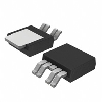
DPAK 5−PIN
DT SUFFIX
CASE 175AA
Features
5
1
8
8
1
SOIC−8 FUSED
CASE 751
1
x
y
A
L
Y
WW
G or G
660yx
ALYWW
G
= 5 for 5 V Output, 3 for 3.3 V Output
= 1 for 8 ms, 128 ms Reset Delay,
= 3 for 16 ms, 64 ms Reset Delay
= Assembly Location
= Wafer Lot
= Year
= Work Week
= Pb−Free Package
Applications
• Automotive:
•
Body Control Module
Instrument and Clusters
♦ Occupant Protection and Comfort
♦ Powertrain
Battery Powered Consumer Electronics
♦
ORDERING INFORMATION
♦
See detailed ordering and shipping information in the
dimensions section on page 12 of this data sheet.
IN
VBAT
13.2 V
OUT
NCV8660
OUT
CIN
0.1 mF
COUT
2.2 mF
DT
DT
RO
RO
GND
Figure 1. Application Diagram
© Semiconductor Components Industries, LLC, 2009
January, 2009 − Rev. 9
1
Publication Order Number:
NCV8660/D
�NCV8660
PIN DESCRIPTIONS
Pin
DPAK
SOIC−8
FUSED
Symbol
1
1
IN
Input Supply Voltage. 0.1 mF bypass capacitor to GND at the IC.
2
2
RO
Reset Output. CMOS compatible output. Goes low when VOUT drops by more than 7%
from nominal.
3, Tab
5−8
GND
4
3
DT
5
4
OUT
Function
Ground
Reset Delay Time Select. Short to GND or connect to OUT to select time.
Regulated Voltage Output. 2.2 mF to ground for typical applications.
IN
OUT
Current Limit
and Thermal
Shutdown
+
−
Vref1
GND
DT
−
Timing
Circuit
+
Vref2
Figure 2. Block Diagram
http://onsemi.com
2
RO
�NCV8660
ABSOLUTE MAXIMUM RATINGS
Symbol
Min
Max
Unit
Input Voltage (IN)
Rating
VIN
−0.3
40
V
Input Current
IIN
−1.0
−
mA
−0.3
−0.3
5.5
16
Output Voltage (OUT)
DC
Transient, t < 10 s (Note 1)
VOUT
V
Output Current (OUT)
IOUT
−1.0
Current
Limited
mA
Storage Temperature Range
TSTG
−55
150
°C
DT (Reset Delay Time Select) Voltage (Note 2)
VDT
−0.3
16
V
DT (Reset Delay Time Select) Current (Note 2)
IDT
−1.0
1.0
mA
RO (Reset Output) Voltage
DC
Transient, t < 10 s
VRO
−0.3
−0.3
5.5
16
RO (Reset Output) Current
IRO
−1.0
1.0
mA
ESD Capability, Human Body Model (Note 3)
ESDHB
−2.0
2.0
kV
ESD Capability, Machine Model (Note 3)
ESDMM
−200
200
V
ESD Capability, Charged Device Model (Note 3)
ESDCDM
−1.0
1.0
kV
V
ESD CAPABILITY
THERMAL RESISTANCE
Junction−to−Case (Note 4)
DPAK 5
RqJC
15
°C/W
Junction−to−Ambient (Note 4)
DPAK 5
RqJA
66
°C/W
Junction−to−Tab (Note 4)
DPAK 5
RqJT
4.0
°C/W
Junction−to−Ambient (Note 4)
SOIC−8 FUSED
RqJA
104
°C/W
Junction−to−Lead (pin 6) (Note 4)
SOIC−8 FUSED
RqJT
33
°C/W
DPAK 5
SOIC−8 FUSED
MSL
1
3
−
LEAD SOLDERING TEMPERATURE AND MSL
Moisture Sensitivity Level
Lead Temperature Soldering: SMD style only, Reflow (Note 5)
Pb−Free Part 60 − 150 sec above 217°C, 40 sec max at peak
SLD
−
265 peak
°C
Stresses exceeding Maximum Ratings may damage the device. Maximum Ratings are stress ratings only. Functional operation above the
Recommended Operating Conditions is not implied. Extended exposure to stresses above the Recommended Operating Conditions may affect
device reliability.
1. The output voltage must not exceed the input voltage.
2. External resistor required to minimize current to less than 1 mA when the control voltage is above 16 V.
3. This device series incorporates ESD protection and is tested by the following methods:
ESD HBM tested per AEC−Q100−002 (EIA/JESD22−A114)
ESD MM tested per AEC−Q100−003 (EIA/JESD22−A115)
ESD CDM tested per EIA/JESD22/C101, Field Induced Charge Model
4. Values represented typical steady−state thermal performance on 1 oz. copper FR4 PCB with 1 in2 copper area.
5. Per IPC / JEDEC J−STD−020C.
OPERATING RANGE
Pin Symbol, Parameter
Symbol
Min
Max
Unit
VIN, Input Voltage Operating Range
VIN
4.5
40
V
Junction Temperature Range
TJ
−40
150
°C
http://onsemi.com
3
�NCV8660
ELECTRICAL CHARACTERISTICS 5.5 V < VIN < 40 V, −40°C ≤ TJ ≤ +150°C, unless otherwise specified
Characteristic
Symbol
Conditions
Min
Typ
Max
Unit
Iq
100mA < IOUT < 150mA, VIN = 13.2V, TJ = 25°C
−
25
30
mA
GENERAL
Quiescent Current
−
−
40
Thermal Shutdown (Note 6)
TSD
150
175
195
°C
Thermal Hysteresis (Note 6)
THYS
−
25
−
°C
6 V ≤ VIN ≤ 16 V, 0.1 mA ≤ IOUT ≤ 150 mA
4.9
5.0
5.1
V
6 V ≤ VIN ≤ 40 V, 0.1 mA ≤ IOUT ≤ 100 mA
4.9
5.0
5.1
5.6 V ≤ VIN ≤ 16 V, 0 mA ≤ IOUT ≤ 150 mA,
−40°C ≤ TJ ≤ +125°C
4.9
5.0
5.1
5.5 V ≤ VIN ≤ 16 V, 0.1 mA ≤ IOUT ≤ 150 mA
3.234
3.3
3.366
5.5 V ≤ VIN ≤ 40 V, 0.1 mA ≤ IOUT ≤ 100 mA
3.234
3.3
3.366
OUT = 96% x VOUT nominal
205
−
525
mA
OUT = 0 V
205
−
525
mA
100mA < IOUT < 150mA, VIN = 13.2V, TJ ≤ 85°C
OUT
Output Voltage
VOUT
Output Voltage
VOUT
Output Current Limit
ICL
Output Current Limit,
Short Circuit
ISCKT
V
Load Regulation
DVOUT
VIN = 13.2 V, IOUT = 0.1 mA to 150 mA
−40
10
40
mV
Line Regulation
DVOUT
IOUT = 5 mA, VIN = 6 V to 28 V
−20
0
20
mV
IOUT = 100 mA, (Note 7)
VDR = VIN – VOUT, (DVOUT = −100 mV)
−
0.225
0.45
V
IOUT = 150 mA, (Note 7)
VDR = VIN – VOUT, (DVOUT = −100 mV)
−
0.30
0.60
Dropout Voltage − 5.0 V Only
Output Load Capacitance
Power Supply Ripple Rejection
VDR
CO
Output capacitance for stability
2.2
−
−
mF
PSRR
VIN = 13.2 V, 0.5 VPP, 100 Hz
−
60
−
dB
2
−
−
−
−
0.8
V
V
DT = 5 V
−
−
1.0
mA
VOUT decreasing
90
93
96
%VOUT
−
2.0
−
%VOUT
DT (Reset Delay Time Select)
Threshold Voltage
High
Low
Input Current
RO, Reset Output
RESET Threshold
RESET Threshold Hysteresis
VRf
VRhys
RO Output Low
VRL
10 kW RESET to OUT, VOUT = 4.5 V
RO Output High (OUT−RO)
VRH
10 kW RESET to GND
Reset Reaction Time
tRR
VIN_RT
Input Voltage Reset Threshold
−
0.2
0.4
V
VOUT
−0.4
VOUT
−0.2
VOUT
V
VOUT into UV to RESET Low
16
25
38
msec
VIN Decreasing, VOUT > VRT
−
3.8
4.25
V
5.0
10
20
40
80
8.0
16
32
64
128
11.5
23
46
92
184
RESET Delay with DT Selection
Delay Time Out of RESET
− 8 ms version
− 16 ms version
− 32 ms version
− 64 ms version
− 128 ms version
tdRx
VOUT into regulation to RO High
msec
6. Not production tested, guaranteed by design.
7. Dropout at a given current level is defined as the voltage difference of VIN to VOUT with VIN decreasing until the output drops by 100 mV.
http://onsemi.com
4
�NCV8660
5.0
3.315
4.995
3.310
3.305
4.99
OUTPUT VOLTAGE (V)
OUTPUT VOLTAGE (V)
TYPICAL OPERATING CHARACTERISTICS
4.985
4.98
4.975
4.97
4.965
80
60
100 120
3.295
3.290
3.285
3.280
3.275
3.270
3.265
Iout = 0 mA, 150 mA
3.260
0
20
40
−40 −20
140 160
Figure 4. Output Voltage vs. Temperature
(OUT = 3.3 V)
4.995
3.305
4.99
4.985
4.98
−40°C
4.975
4.97
4.965
150°C
0
20
40
60
80
25°C
3.300
25°C
4.96
100
120
140
3.295
3.285
3.280
3.275
3.270
150°C
3.265
3.260
3.255
160
−40°C
3.290
0
20
40
Figure 5. Output Voltage vs. Output Current
(OUT = 5 V)
80
100
120
140
160
Figure 6. Output Voltage vs. Output Current
(OUT = 3.3 V)
3.5
5
3.0
OUTPUT VOLTAGE (V)
6
4
−40°C
3
60
OUTPUT CURRENT (mA)
OUTPUT CURRENT (mA)
OUTPUT VOLTAGE (V)
140 160
Figure 3. Output Voltage vs. Temperature
(OUT = 5 V)
3.310
2
25°C
1
0
100 120
80
TEMPERATURE (°C)
5.0
4.955
60
TEMPERATURE (°C)
OUTPUT VOLTAGE (V)
OUTPUT VOLTAGE (V)
Iout = 0 mA, 150 mA
4.96
−40 −20
0
20
40
3.300
2.5
2.0
1.5
150°C 25°C
−40°C
1.0
0.5
150°C
0
0.5
1
1.5
2
2.5
3
3.5
4
4.5
5
5.5
0
6
0
0.5
1
1.5
2
2.5
3
3.5
4
4.5
5
5.5
INPUT VOLTAGE (V)
INPUT VOLTAGE (V)
Figure 7. Output Voltage vs. Input Voltage
(RLOAD = 51 k, Iout = 100 mA, OUT = 5 V)
Figure 8. Output Voltage vs. Input Voltage
(RLOAD = 51 k, Iout = 100 mA, OUT = 3.3 V)
http://onsemi.com
5
6
�NCV8660
380
600
370
500
DROPOUT VOLTAGE (mV)
CURRENT LIMIT (mA)
TYPICAL OPERATING CHARACTERISTICS
360
350
340
330
320
310
−40 −20
400
200
25°C
100
−40°C
Vin = 13.2 V
0
20
40
60
80
100 120
150°C
300
0
140 160
0
25
50
TEMPERATURE (°C)
Figure 9. Current Limit vs. Temperature
125
150
40
150 mA
35
500
125 mA
1 mA
400
100 mA
300
75 mA
200
50 mA
25 mA
100
10 mA
0
−40 −20
0
20
40
60
80
100 120
30
25
20
15
10
5
0
140 160
Iout = 0 mA
0
2
4
6
TEMPERATURE (°C)
8
10
12
14
16
INPUT VOLTAGE (V)
Figure 11. Dropout Voltage vs. Temperature
Figure 12. Quiescent Current vs. Input Voltage
35
29
QUIESCENT CURRENT (mA)
28.5
QUIESCENT CURRENT (mA)
100
Figure 10. Dropout Voltage vs. Output Current
QUIESCENT CURRENT (mA)
DROPOUT VOLTAGE (mV)
600
75
OUTPUT CURRENT (mA)
28
27.5
27
26.5
26
25.5
25
24.5
24
23.5
−40 −20
0
20
40
60
80
100 120
25°C
25
−40°C
20
15
10
5
0
140 160
150°C
30
0
20
40
60
80
100
120
140
160
TEMPERATURE (°C)
OUTPUT CURRENT (mA)
Figure 13. Quiescent Current vs. Temperature
Figure 14. Quiescent Current vs. Output Current
http://onsemi.com
6
�NCV8660
TYPICAL OPERATING CHARACTERISTICS
Figure 15. Load Transient
(VIN = 13.2 V, OUT = 5 V)
Figure 17. Load Transient
(VIN = 13.2 V, OUT = 3.3 V)
IN
OUT
Cout = 2.2 mF
Iout = 150 mA
Figure 16. Line Transient (OUT = 5 V)
Figure 18. Line Transient (OUT = 3.3 V)
http://onsemi.com
7
�NCV8660
80
80
70
70
60
60
MAG (dB)
MAG (dB)
TYPICAL OPERATING CHARACTERISTICS
50
40
30
20
0
10
100
40
30
20
VIN = 13.2 V
COUT = 4.7 mF
IOUT = 100 mA
10
50
VIN = 13.2 V
COUT = 4.7 mF
IOUT = 150 mA
10
0
1k
10 k
100 k
1M
10 M
10
100
1k
FREQUENCY
Figure 19. Ripple Rejection vs. Frequency
(VIN = 13.2 V, IOUT = 100 mA)
10000
125°C
1M
10 M
Unstable Region
125°C
ESR (W)
100
10
Stable Region
10
1
Stable Region
1
0.1
0.01
25°C
−40°C
1000
0
20
40
60
80
100
120
140
Vin = 13.2 V
CLOAD = 2.2 mF
0.1
Vin = 13.2 V
CLOAD = 2.2 mF
0.01
160
0
20
40
60
80
100
120
140
OUTPUT CURRENT (mA)
OUTPUT CURRENT (mA)
Figure 21. Output Capacitor ESR vs. Output
Current (OUT = 5 V)
Figure 22. Output Capacitor ESR vs. Output
Current (OUT = 3.3 V)
5.5
5.0
4.5
OUTPUT VOLTAGE (V)
ESR (W)
10000
−40°C
100
100 k
Figure 20. Ripple Rejection vs. Frequency
(VIN = 13.2 V, IOUT = 150 mA)
Unstable Region
25°C
1000
10 k
FREQUENCY
Temperature Increasing
4.0
3.5
Temperature Decreasing
3.0
2.5
2.0
1.5
1.0
0.5
0
25
50
100
75
125
150
175
TEMPERATURE (°C)
Figure 23. Thermal Shutdown vs. Temperature
http://onsemi.com
8
160
�NCV8660
DETAILED OPERATING DESCRIPTION
General
Current Limit
The NCV8660 is a 5 V and 3.3 V linear regulator
providing low drop−out voltage for 150 mA at low quiescent
current levels. Also featured in this part is a reset output with
selectable delay times. Delay times are selectable via part
selection and control through the Delay Time Select (DT)
pin. No pull−up resistor is needed on the reset output (RO).
Pull−up and pull−down capability are included. Only a small
bypass capacitor on the input (IN) supply pin and output
(OUT) voltage pin are required for normal operation.
Thermal shutdown functionality protects the IC from
damage caused from excessively high temperatures
appearing on the IC.
Current limit is provided on OUT to protect the IC. The
minimum specification is 205 mA. Current limit is specified
under two conditions (OUT = 96% x OUT nominal) and
(OUT = 0 V). No fold−back circuitry exists. Any measured
differences can be attributed to change in die temperature.
The part may be operated up to 205 mA provided thermal die
temperature is considered and is kept below 150°C.
Degradation of electrical parameters at this current is
expected at these elevated levels. A reset (RO) will not occur
with a load less than 205 mA.
Reset Output
A reset signal is provided on the Reset Output (RO) pin to
provide feedback to the microprocessor of an out of
regulation condition. This is in the form of a logic signal on
RO. Output (OUT) voltage conditions below the RESET
threshold cause RO to go low. The RO integrity is
maintained down to OUT = 1.0 V.
The Reset Output (RO) circuitry includes an active
internal pullup to the output (OUT) as shown in Figure 24.
No external pullup is neccessary.
Output Voltage
Output stability is determined by the capacitor selected
from OUT to GND. The NCV8660 has been designed to
work with low ESR (equivalent series resistance) ceramic
capacitors. The device is extremely stable using virtually
any capacitor 2.2 mF and above. Reference the Output
Capacitor Stability graph in Figure 21.
The output capacitor value will affect overshoot during
power−up. A lower value capacitor will cause higher
overshoot on the output. System evaluation should be
performed with minimum loading for evaluation of
overshoot.
Selection of process technology for the NCV8660 allows
for low quiescent current independent of loading. Quiescent
current will remain flat across the entire range of loads
providing a low quiescent current condition in standby and
under heavy loads. This is highly beneficial to systems
requiring microprocessor interrupts during standby mode as
duty cycle and load changes have no impact on the standby
current. Reference Figure 14 for Quiescent Current vs
Output Current.
OUT
RO
Reset
Control
Signal
Figure 24. Reset Output Circuitry
http://onsemi.com
9
�NCV8660
IN
t
Reset Delay Time
OUT
t < Reset Reaction Time
OUT Reset Threshold plus Hysteresis
OUT Reset Threshold
t
RO
t
Reset
Threshold
Plus
Hysteresis
Thermal
Shutdown
Voltage Dip
at Input
Reset Delay Time
Secondary
Spike
Overload
at Output
Reset Delay Time
Thermal Shutdown
minus
Thermal Hysteresis
Figure 25. Reset Timing
During power−up (or restoring OUT voltage from a reset
event), the OUT voltage must be maintained above the Reset
threshold for the Reset Delay time before RO goes high. The
time for Reset Delay is determined by the choice of IC and
the state of the DT pin.
The Delay Time select (DT) pin is logic level controlled
and provides Reset Delay time per the chart. Note the DT pin
is sampled only when RO is low, and changes to the DT pin
when RO is high will not effect the reset delay time.
Thermal Shutdown
When the die temperature exceeds the Thermal Shutdown
threshold, a Thermal Shutdown event is detected OUT is
turned off, and RO goes low. The IC will remain in this state
until the die temperature moves below the shutdown
threshold (175°C typical) minus the hysteresis factor (25°C
typical). The output will then turn back on and RO will go
high after the RESET Delay time.
Reset Delay Time Select
Selection of the NCV8660 device and the state of the DT
pin determines the available Reset Delay times. The part is
designed for use with DT tied to ground or OUT, but may be
controlled by any logic signal which provides a threshold
between 0.8 V and 2 V. The default condition for an open DT
pin is the slower Reset time (DT = GND condition). Times
are in pairs and are highlighted in the chart below. Consult
factory for availability.
DT=GND
DT=OUT
Reset Time
Reset Time
NCV86601
8 ms
128 ms
NCV86602
8 ms
32 ms
NCV86603
16 ms
64 ms
NCV86604
32 ms
128 ms
Reset
Reaction
Time
http://onsemi.com
10
�NCV8660
80
Theta JA curve
70
60
50
0
100
R(t), (°C/W)
10
1
0.1
100
200
300
400
500
600
170
1.6
160
1.4
150
1.2
1.0
0.8
0.6
ThetaJA (°C/W)
90
1.8
1.2
Power curve with PCB 1 oz cu
140
130
120
110
0.4
100
0.2
90
80
0
700
1.3
MAX POWER (W)
Power curve with PCB 1 oz cu
MAX POWER (W)
ThetaJA (°C/W)
100
40
180
2.0
110
Theta JA curve
1.1
1.0
0.9
0.8
0
100
200
300
400
500
600
COPPER HEAT SPREADER AREA (mm2)
COPPER HEAT SPREADER AREA (mm2)
Figure 26. RqJA vs. PCB Copper Area (DPAK)
Figure 28. RqJA vs. PCB Copper Area
(SOIC−8 Fused)
0.7
700
0.5
0.2
0.1
0.05
0.02
0.01
Single Pulse
0.01
0.001
0.000001
Psi Tab−A
0.00001
0.0001
0.001
0.01
0.1
PULSE TIME (sec)
1
10
100
1000
10
100
1000
Figure 27. Transient Thermal Response (DPAK)
Cu Area = 645 mm2
100
R(t), (°C/W)
0.5
0.2
10 0.1
0.05
0.02
1
0.01
Single Pulse
0.1
0.01
0.001
0.000001
Psi L−A
0.00001
0.0001
0.001
0.01
0.1
PULSE TIME (sec)
1
Figure 29. Transient Thermal Response (SOIC−8 Fused)
Cu Area = 645 mm2
http://onsemi.com
11
�NCV8660
ORDERING INFORMATION
Reset Delay Time,
DT to GND
Reset Delay Time,
DT to OUT
NCV86601DT50RKG
8 ms
128 ms
NCV86602DT50RKG
8 ms
32 ms
NCV86603DT50RKG
16 ms
64 ms
NCV86604DT50RKG
32 ms
128 ms
NCV86601D50G
8 ms
128 ms
NCV86601D50R2G
8 ms
128 ms
NCV86602D50R2G
8 ms
32 ms
NCV86603D50R2G
16 ms
64 ms
NCV86604D50R2G
32 ms
128 ms
NCV86601DT33RKG
8 ms
128 ms
NCV86602DT33RKG
8 ms
32 ms
NCV86603DT33RKG
16 ms
64 ms
32 ms
128 ms
8 ms
128 ms
NCV86602D33R2G
8 ms
32 ms
NCV86603D33R2G
16 ms
64 ms
NCV86604D33R2G
32 ms
128 ms
Device
NCV86604DT33RKG
NCV86601D33R2G
Output Voltage
5.0 V
3.3 V
Package
Shipping†
DPAK
(Pb−Free)
2500 / Tape & Reel
98 Units / Rail
SOIC−8 FUSED
(Pb−Free)
2500 / Tape & Reel
DPAK
(Pb−Free)
2500 / Tape & Reel
SOIC−8 FUSED
(Pb−Free)
2500 / Tape & Reel
†For information on tape and reel specifications, including part orientation and tape sizes, please refer to our Tape and Reel Packaging
Specification Brochure, BRD8011/D.
http://onsemi.com
12
�MECHANICAL CASE OUTLINE
PACKAGE DIMENSIONS
DPAK−5, CENTER LEAD CROP
CASE 175AA
ISSUE B
DATE 15 MAY 2014
SCALE 1:1
−T−
C
B
V
NOTES:
1. DIMENSIONING AND TOLERANCING
PER ANSI Y14.5M, 1982.
2. CONTROLLING DIMENSION: INCH.
SEATING
PLANE
E
R
R1
Z
A
S
12 3 4 5
U
K
F
J
L
H
D
G
5 PL
0.13 (0.005)
M
T
2.2
0.086
0.34 5.36
0.013 0.217
5.8
0.228
10.6
0.417
0.8
0.031
SCALE 4:1
mm Ǔ
ǒinches
*For additional information on our Pb−Free strategy and soldering
details, please download the ON Semiconductor Soldering and
Mounting Techniques Reference Manual, SOLDERRM/D.
DOCUMENT NUMBER:
DESCRIPTION:
98AON12855D
INCHES
MIN
MAX
0.235 0.245
0.250 0.265
0.086 0.094
0.020 0.028
0.018 0.023
0.024 0.032
0.180 BSC
0.034 0.040
0.018 0.023
0.102 0.114
0.045 BSC
0.170 0.190
0.185 0.210
0.025 0.040
0.020
−−−
0.035 0.050
0.155 0.170
MILLIMETERS
MIN
MAX
5.97
6.22
6.35
6.73
2.19
2.38
0.51
0.71
0.46
0.58
0.61
0.81
4.56 BSC
0.87
1.01
0.46
0.58
2.60
2.89
1.14 BSC
4.32
4.83
4.70
5.33
0.63
1.01
0.51
−−−
0.89
1.27
3.93
4.32
GENERIC
MARKING DIAGRAMS*
RECOMMENDED
SOLDERING FOOTPRINT*
6.4
0.252
DIM
A
B
C
D
E
F
G
H
J
K
L
R
R1
S
U
V
Z
XXXXXXG
ALYWW
AYWW
XXX
XXXXXG
IC
Discrete
XXXXXX
A
L
Y
WW
G
= Device Code
= Assembly Location
= Wafer Lot
= Year
= Work Week
= Pb−Free Package
*This information is generic. Please refer to
device data sheet for actual part marking.
Pb−Free indicator, “G” or microdot “ G”,
may or may not be present.
Electronic versions are uncontrolled except when accessed directly from the Document Repository.
Printed versions are uncontrolled except when stamped “CONTROLLED COPY” in red.
DPAK−5 CENTER LEAD CROP
PAGE 1 OF 1
ON Semiconductor and
are trademarks of Semiconductor Components Industries, LLC dba ON Semiconductor or its subsidiaries in the United States and/or other countries.
ON Semiconductor reserves the right to make changes without further notice to any products herein. ON Semiconductor makes no warranty, representation or guarantee regarding
the suitability of its products for any particular purpose, nor does ON Semiconductor assume any liability arising out of the application or use of any product or circuit, and specifically
disclaims any and all liability, including without limitation special, consequential or incidental damages. ON Semiconductor does not convey any license under its patent rights nor the
rights of others.
© Semiconductor Components Industries, LLC, 2019
www.onsemi.com
�MECHANICAL CASE OUTLINE
PACKAGE DIMENSIONS
SOIC−8 NB
CASE 751−07
ISSUE AK
8
1
SCALE 1:1
−X−
DATE 16 FEB 2011
NOTES:
1. DIMENSIONING AND TOLERANCING PER
ANSI Y14.5M, 1982.
2. CONTROLLING DIMENSION: MILLIMETER.
3. DIMENSION A AND B DO NOT INCLUDE
MOLD PROTRUSION.
4. MAXIMUM MOLD PROTRUSION 0.15 (0.006)
PER SIDE.
5. DIMENSION D DOES NOT INCLUDE DAMBAR
PROTRUSION. ALLOWABLE DAMBAR
PROTRUSION SHALL BE 0.127 (0.005) TOTAL
IN EXCESS OF THE D DIMENSION AT
MAXIMUM MATERIAL CONDITION.
6. 751−01 THRU 751−06 ARE OBSOLETE. NEW
STANDARD IS 751−07.
A
8
5
S
B
0.25 (0.010)
M
Y
M
1
4
−Y−
K
G
C
N
X 45 _
SEATING
PLANE
−Z−
0.10 (0.004)
H
M
D
0.25 (0.010)
M
Z Y
S
X
J
S
8
8
1
1
IC
4.0
0.155
XXXXX
A
L
Y
W
G
IC
(Pb−Free)
= Specific Device Code
= Assembly Location
= Wafer Lot
= Year
= Work Week
= Pb−Free Package
XXXXXX
AYWW
1
1
Discrete
XXXXXX
AYWW
G
Discrete
(Pb−Free)
XXXXXX = Specific Device Code
A
= Assembly Location
Y
= Year
WW
= Work Week
G
= Pb−Free Package
*This information is generic. Please refer to
device data sheet for actual part marking.
Pb−Free indicator, “G” or microdot “G”, may
or may not be present. Some products may
not follow the Generic Marking.
1.270
0.050
SCALE 6:1
INCHES
MIN
MAX
0.189
0.197
0.150
0.157
0.053
0.069
0.013
0.020
0.050 BSC
0.004
0.010
0.007
0.010
0.016
0.050
0 _
8 _
0.010
0.020
0.228
0.244
8
8
XXXXX
ALYWX
G
XXXXX
ALYWX
1.52
0.060
0.6
0.024
MILLIMETERS
MIN
MAX
4.80
5.00
3.80
4.00
1.35
1.75
0.33
0.51
1.27 BSC
0.10
0.25
0.19
0.25
0.40
1.27
0_
8_
0.25
0.50
5.80
6.20
GENERIC
MARKING DIAGRAM*
SOLDERING FOOTPRINT*
7.0
0.275
DIM
A
B
C
D
G
H
J
K
M
N
S
mm Ǔ
ǒinches
*For additional information on our Pb−Free strategy and soldering
details, please download the ON Semiconductor Soldering and
Mounting Techniques Reference Manual, SOLDERRM/D.
STYLES ON PAGE 2
DOCUMENT NUMBER:
DESCRIPTION:
98ASB42564B
SOIC−8 NB
Electronic versions are uncontrolled except when accessed directly from the Document Repository.
Printed versions are uncontrolled except when stamped “CONTROLLED COPY” in red.
PAGE 1 OF 2
onsemi and
are trademarks of Semiconductor Components Industries, LLC dba onsemi or its subsidiaries in the United States and/or other countries. onsemi reserves
the right to make changes without further notice to any products herein. onsemi makes no warranty, representation or guarantee regarding the suitability of its products for any particular
purpose, nor does onsemi assume any liability arising out of the application or use of any product or circuit, and specifically disclaims any and all liability, including without limitation
special, consequential or incidental damages. onsemi does not convey any license under its patent rights nor the rights of others.
© Semiconductor Components Industries, LLC, 2019
www.onsemi.com
�SOIC−8 NB
CASE 751−07
ISSUE AK
DATE 16 FEB 2011
STYLE 1:
PIN 1. EMITTER
2. COLLECTOR
3. COLLECTOR
4. EMITTER
5. EMITTER
6. BASE
7. BASE
8. EMITTER
STYLE 2:
PIN 1. COLLECTOR, DIE, #1
2. COLLECTOR, #1
3. COLLECTOR, #2
4. COLLECTOR, #2
5. BASE, #2
6. EMITTER, #2
7. BASE, #1
8. EMITTER, #1
STYLE 3:
PIN 1. DRAIN, DIE #1
2. DRAIN, #1
3. DRAIN, #2
4. DRAIN, #2
5. GATE, #2
6. SOURCE, #2
7. GATE, #1
8. SOURCE, #1
STYLE 4:
PIN 1. ANODE
2. ANODE
3. ANODE
4. ANODE
5. ANODE
6. ANODE
7. ANODE
8. COMMON CATHODE
STYLE 5:
PIN 1. DRAIN
2. DRAIN
3. DRAIN
4. DRAIN
5. GATE
6. GATE
7. SOURCE
8. SOURCE
STYLE 6:
PIN 1. SOURCE
2. DRAIN
3. DRAIN
4. SOURCE
5. SOURCE
6. GATE
7. GATE
8. SOURCE
STYLE 7:
PIN 1. INPUT
2. EXTERNAL BYPASS
3. THIRD STAGE SOURCE
4. GROUND
5. DRAIN
6. GATE 3
7. SECOND STAGE Vd
8. FIRST STAGE Vd
STYLE 8:
PIN 1. COLLECTOR, DIE #1
2. BASE, #1
3. BASE, #2
4. COLLECTOR, #2
5. COLLECTOR, #2
6. EMITTER, #2
7. EMITTER, #1
8. COLLECTOR, #1
STYLE 9:
PIN 1. EMITTER, COMMON
2. COLLECTOR, DIE #1
3. COLLECTOR, DIE #2
4. EMITTER, COMMON
5. EMITTER, COMMON
6. BASE, DIE #2
7. BASE, DIE #1
8. EMITTER, COMMON
STYLE 10:
PIN 1. GROUND
2. BIAS 1
3. OUTPUT
4. GROUND
5. GROUND
6. BIAS 2
7. INPUT
8. GROUND
STYLE 11:
PIN 1. SOURCE 1
2. GATE 1
3. SOURCE 2
4. GATE 2
5. DRAIN 2
6. DRAIN 2
7. DRAIN 1
8. DRAIN 1
STYLE 12:
PIN 1. SOURCE
2. SOURCE
3. SOURCE
4. GATE
5. DRAIN
6. DRAIN
7. DRAIN
8. DRAIN
STYLE 13:
PIN 1. N.C.
2. SOURCE
3. SOURCE
4. GATE
5. DRAIN
6. DRAIN
7. DRAIN
8. DRAIN
STYLE 14:
PIN 1. N−SOURCE
2. N−GATE
3. P−SOURCE
4. P−GATE
5. P−DRAIN
6. P−DRAIN
7. N−DRAIN
8. N−DRAIN
STYLE 15:
PIN 1. ANODE 1
2. ANODE 1
3. ANODE 1
4. ANODE 1
5. CATHODE, COMMON
6. CATHODE, COMMON
7. CATHODE, COMMON
8. CATHODE, COMMON
STYLE 16:
PIN 1. EMITTER, DIE #1
2. BASE, DIE #1
3. EMITTER, DIE #2
4. BASE, DIE #2
5. COLLECTOR, DIE #2
6. COLLECTOR, DIE #2
7. COLLECTOR, DIE #1
8. COLLECTOR, DIE #1
STYLE 17:
PIN 1. VCC
2. V2OUT
3. V1OUT
4. TXE
5. RXE
6. VEE
7. GND
8. ACC
STYLE 18:
PIN 1. ANODE
2. ANODE
3. SOURCE
4. GATE
5. DRAIN
6. DRAIN
7. CATHODE
8. CATHODE
STYLE 19:
PIN 1. SOURCE 1
2. GATE 1
3. SOURCE 2
4. GATE 2
5. DRAIN 2
6. MIRROR 2
7. DRAIN 1
8. MIRROR 1
STYLE 20:
PIN 1. SOURCE (N)
2. GATE (N)
3. SOURCE (P)
4. GATE (P)
5. DRAIN
6. DRAIN
7. DRAIN
8. DRAIN
STYLE 21:
PIN 1. CATHODE 1
2. CATHODE 2
3. CATHODE 3
4. CATHODE 4
5. CATHODE 5
6. COMMON ANODE
7. COMMON ANODE
8. CATHODE 6
STYLE 22:
PIN 1. I/O LINE 1
2. COMMON CATHODE/VCC
3. COMMON CATHODE/VCC
4. I/O LINE 3
5. COMMON ANODE/GND
6. I/O LINE 4
7. I/O LINE 5
8. COMMON ANODE/GND
STYLE 23:
PIN 1. LINE 1 IN
2. COMMON ANODE/GND
3. COMMON ANODE/GND
4. LINE 2 IN
5. LINE 2 OUT
6. COMMON ANODE/GND
7. COMMON ANODE/GND
8. LINE 1 OUT
STYLE 24:
PIN 1. BASE
2. EMITTER
3. COLLECTOR/ANODE
4. COLLECTOR/ANODE
5. CATHODE
6. CATHODE
7. COLLECTOR/ANODE
8. COLLECTOR/ANODE
STYLE 25:
PIN 1. VIN
2. N/C
3. REXT
4. GND
5. IOUT
6. IOUT
7. IOUT
8. IOUT
STYLE 26:
PIN 1. GND
2. dv/dt
3. ENABLE
4. ILIMIT
5. SOURCE
6. SOURCE
7. SOURCE
8. VCC
STYLE 29:
PIN 1. BASE, DIE #1
2. EMITTER, #1
3. BASE, #2
4. EMITTER, #2
5. COLLECTOR, #2
6. COLLECTOR, #2
7. COLLECTOR, #1
8. COLLECTOR, #1
STYLE 30:
PIN 1. DRAIN 1
2. DRAIN 1
3. GATE 2
4. SOURCE 2
5. SOURCE 1/DRAIN 2
6. SOURCE 1/DRAIN 2
7. SOURCE 1/DRAIN 2
8. GATE 1
DOCUMENT NUMBER:
DESCRIPTION:
98ASB42564B
SOIC−8 NB
STYLE 27:
PIN 1. ILIMIT
2. OVLO
3. UVLO
4. INPUT+
5. SOURCE
6. SOURCE
7. SOURCE
8. DRAIN
STYLE 28:
PIN 1. SW_TO_GND
2. DASIC_OFF
3. DASIC_SW_DET
4. GND
5. V_MON
6. VBULK
7. VBULK
8. VIN
Electronic versions are uncontrolled except when accessed directly from the Document Repository.
Printed versions are uncontrolled except when stamped “CONTROLLED COPY” in red.
PAGE 2 OF 2
onsemi and
are trademarks of Semiconductor Components Industries, LLC dba onsemi or its subsidiaries in the United States and/or other countries. onsemi reserves
the right to make changes without further notice to any products herein. onsemi makes no warranty, representation or guarantee regarding the suitability of its products for any particular
purpose, nor does onsemi assume any liability arising out of the application or use of any product or circuit, and specifically disclaims any and all liability, including without limitation
special, consequential or incidental damages. onsemi does not convey any license under its patent rights nor the rights of others.
© Semiconductor Components Industries, LLC, 2019
www.onsemi.com
�onsemi,
, and other names, marks, and brands are registered and/or common law trademarks of Semiconductor Components Industries, LLC dba “onsemi” or its affiliates
and/or subsidiaries in the United States and/or other countries. onsemi owns the rights to a number of patents, trademarks, copyrights, trade secrets, and other intellectual property.
A listing of onsemi’s product/patent coverage may be accessed at www.onsemi.com/site/pdf/Patent−Marking.pdf. onsemi reserves the right to make changes at any time to any
products or information herein, without notice. The information herein is provided “as−is” and onsemi makes no warranty, representation or guarantee regarding the accuracy of the
information, product features, availability, functionality, or suitability of its products for any particular purpose, nor does onsemi assume any liability arising out of the application or use
of any product or circuit, and specifically disclaims any and all liability, including without limitation special, consequential or incidental damages. Buyer is responsible for its products
and applications using onsemi products, including compliance with all laws, regulations and safety requirements or standards, regardless of any support or applications information
provided by onsemi. “Typical” parameters which may be provided in onsemi data sheets and/or specifications can and do vary in different applications and actual performance may
vary over time. All operating parameters, including “Typicals” must be validated for each customer application by customer’s technical experts. onsemi does not convey any license
under any of its intellectual property rights nor the rights of others. onsemi products are not designed, intended, or authorized for use as a critical component in life support systems
or any FDA Class 3 medical devices or medical devices with a same or similar classification in a foreign jurisdiction or any devices intended for implantation in the human body. Should
Buyer purchase or use onsemi products for any such unintended or unauthorized application, Buyer shall indemnify and hold onsemi and its officers, employees, subsidiaries, affiliates,
and distributors harmless against all claims, costs, damages, and expenses, and reasonable attorney fees arising out of, directly or indirectly, any claim of personal injury or death
associated with such unintended or unauthorized use, even if such claim alleges that onsemi was negligent regarding the design or manufacture of the part. onsemi is an Equal
Opportunity/Affirmative Action Employer. This literature is subject to all applicable copyright laws and is not for resale in any manner.
PUBLICATION ORDERING INFORMATION
LITERATURE FULFILLMENT:
Email Requests to: orderlit@onsemi.com
onsemi Website: www.onsemi.com
◊
TECHNICAL SUPPORT
North American Technical Support:
Voice Mail: 1 800−282−9855 Toll Free USA/Canada
Phone: 011 421 33 790 2910
Europe, Middle East and Africa Technical Support:
Phone: 00421 33 790 2910
For additional information, please contact your local Sales Representative
�