NLAS4717EP
4.5�W High Bandwidth, Dual
SPDT Analog Switch
The NLAS4717EP is an advanced CMOS analog switch fabricated
in sub−micron silicon gate CMOS technology. The device is a dual
independent Single Pole Double Throw (SPDT) switch featuring low
RDS(on) of 4.5 � at 3.0 V.
The device also features guaranteed Break−Before−Make (BBM)
switching, assuring the switches never short the driver.
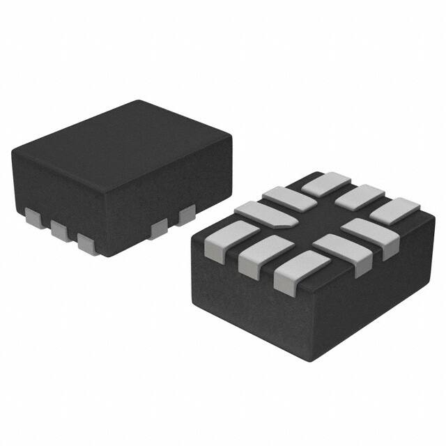
The NLAS4717EP is available in two small size packages:
Microbump: 2.0 x 1.5 mm
WQFN−10:
1.4 x 1.8 mm
4717EP
AYWWG
G
Microbump−10
CASE 489AA
Low RDS(on): 4.5 � @ 3.0 V
Matching Between the Switches 0.5 �
Wide Voltage Range: 1.8 V to 5.5 V
High Bandwidth > 90 MHz
1.65 V to 5.5 V Operating Range
Low Threshold Voltages on Pins 4 and 8 (CTRL Pins)
Ultra−Low Charge Injection 6.0 pC
Low Standby Current: ICC = 1.0 nA (Max) @ TA = 25C
*OVT on Pins 4 and 8 (CTRL Logic Pins)
These are Pb−Free Devices
A1
A
= Assembly Location
Y
= Year
W, WW = Work Week
G
= Pb−Free Package
(Note: Microdot may be in either location)
AWMG
G
1
WQFN−10
CASE 488AQ
AW
= Specific Device Code
M
= Date Code
G
= Pb−Free Device
(Note: Microdot may be in either location)
Typical Applications
MARKING
DIAGRAMS
A1
Features
http://onsemi.com
Cell Phones
PDAs
MP3s
Digital Still Cameras
USB 2.0 Full Speed (USB1.1) − 12 Mbps Compliant
FUNCTION TABLE
IN_
NO_
Important Information
0
OFF
ON
ESD Protection:
1
ON
OFF
Human Body Model (HBM) = 2500 V,
Machine Model (MM) = 200 V
Latchup Max Rating: 200 mA (Per JEDEC EIA/JESD78)
Pin−to−Pin Compatible with MAX4717
NC_
ORDERING INFORMATION
Device
Package
Shipping†
*OVT
NLAS4717EPFCT1G Microbump−10
3000 /
(Pb−Free)
Tape & Reel
Overvoltage Tolerant (OVT) specific pins operate higher than normal
NLAS4717EPMTR2G
supply voltages, with no damage to the devices or to signal integrity.
WQFN−10
(Pb−Free)
3000 /
Tape & Reel
†For information on tape and reel specifications,
including part orientation and tape sizes, please
refer to our Tape and Reel Packaging Specifications
Brochure, BRD8011/D.
Semiconductor Components Industries, LLC, 2011
October, 2011 − Rev. 7
1
Publication Order Number:
NLAS4717EP/D
�NLAS4717EP
GND
B1
A1
NC2
C2
A2
IN2
COM1
C3
A3
COM2
NO1
C4
A4
NO2
NC1
C1
IN1
B4
NO1
VCC
2
1
COM1
3
10
NO2
IN1
4
9
COM2
NC1
5
8
IN2
VCC
Microbump
(Top View)
6
7
GND
NC2
WQFN
(Top View)
Figure 1. Device Circuit Diagrams and Pin Configurations
MAXIMUM RATINGS
Symbol
Parameter
Value
Unit
*0.5 to )7.0
V
*0.5 VIS VCC )0.5
V
*0.5 VI )7.0
V
V+
DC Supply Voltage
VIS
Analog Input Voltage (VNO, VNC, or VCOM) (Note 1)
VIN
Digital Select Input Voltage
IIK
DC Current, Into or Out of Any Pin (Continuous)
100
mA
IPK
Peak Current (10% Duty Cycle)
200
mA
Stresses exceeding Maximum Ratings may damage the device. Maximum Ratings are stress ratings only. Functional operation above the
Recommended Operating Conditions is not implied. Extended exposure to stresses above the Recommended Operating Conditions may affect
device reliability.
1. Signal voltage on NC, NO, and COM exceeding VCC or GND are clamped by the internal diodes. Limit forward diode current to maximum
current rating.
RECOMMENDED OPERATING CONDITIONS
Symbol
Parameter
Min
Max
Unit
1.8
5.5
V
V+
DC Supply Voltage
VIN
Digital Select Input Voltage
GND
5.5
V
VIS
Analog Input Voltage (NC, NO, COM)
GND
VCC
V
TA
Operating Temperature Range
−40
+85
C
tr, tf
Input Rise or Fall Time, SELECT
VCC = 3.3 V 0.3 V
VCC = 5.0 V 0.5 V
0
0
100
20
http://onsemi.com
2
ns/V
�NLAS4717EP
ANALOG SWITCH DC CHARACTERISTICS
−40C to +85C
Symbol
Parameter
Condition
VCC (V)
Min
Max
Unit
VIH
Input Logic High Voltage
VOUT = 0.1 V
1.65 to 2.2
VCC x 0.55
−
V
IOUT 20 �A
2.7 to 3.6
VCC x 0.5
−
4.5 to 5.5
2.0
−
VOUT = −VCC − 0.1 V
1.65 to 2.2
−
VCC x 0.2
IOUT 20 �A
2.7 to 3.6
−
VCC x 0.2
4.5 to 5.5
−
0.8
VIL
Input Logic Low Voltage
V
IIN
Input Leakage Current
VIN = VCC or GND
5.5
−100
+100
nA
VCC
Power Supply Range
All
−
1.65
5.5
V
ICC
Supply Current
VIN = VCC or GND
1.8
−
1.0
�A
IOUT = 0 �A
3.3
−
1.0
5.5
−
1.0
ANALOG SWITCH CHARACTERISTICS − Digital Section (Voltages Referenced to GND)
−40C to +85C
Symbol
Parameter
Condition
VCC (V)
Min
Typ
Max
Unit
RON
ON Resistance
(Note 2)
ICOM = 10 mA
VIS = 0 to VCC
3.0
−
3.2
4.5
�
5.0
−
2.1
3.5
3.0
−
0.1
0.4
5.0
−
0.1
0.4
3.0
−
1.12
1.5
5.0
−
0.55
1.36
3.6
−1.0
0.01
+1.0
5.5
−1.0
0.01
+1.0
3.6
−2.0
0.01
+2.0
5.5
−2.0
0.01
+2.0
�RON
RFLAT[ON]
INO_[OFF]
INC_[OFF]
ON Resistance
Match Between Channels
(Note 2 and 3)
ON Resistance
Flatness
(Note 4)
NO_, NC_
Off−Leakage Current
(Note 5)
ICOM = 10 mA
VIS = 0 to VCC
ICOM = 10 mA
�
�
VIS = 0 to VCC
VCOM = 0.3 V or 3.3 V
nA
VNO or VNC = 0.3 V or 3.3 V
VCOM = 0 V or 5.0 V
VNO or VNC = 0 V or 5.0 V
ICOM_[ON]
COM_
On−Leakage Current
(Note 5)
VCOM = 0.3 V or 3.3 V
VNO or VNC = 0.3 V or 3.3 V
VCOM = 0 V or 5.0 V
VNO or VNC = 0 V or 5.0 V
http://onsemi.com
3
nA
�NLAS4717EP
ANALOG SWITCH AC CHARACTERISTICS
−40C to +85C
Symbol
Parameter
Condition
VCC (V)
Min
Typ
Max
Unit
tON
Turn−On Time
VNC_, VNO_ = VIH or VIL
1.8 to 5.5
−
−
30
nS
1.8 to 5.5
−
−
40
nS
−
−
8.0
−
nS
−
−
0.15
2.0
nS
Max
Unit
RL = 300 �, CL = 35 pF
VIN[x] = VIH or VIL
tOFF
Turn−Off Time
VNC_, VNO_ = VIH or VIL
RL = 300 �, CL = 35 pF
VIN[x] = VIH or VIL
tBBM
tSKEW
2.
3.
4.
5.
Break−Before−Make
Time Delay
(Note 5)
Skew
(Note 5)
VNC_, VNO_ = 1.5 V
RL = 300 �, CL = 35 pF
RS = 39 �, CL = 50 pF
RON characterized for VCC range (1.65 V to 5.5 V).
�RON = RON(MAX) − RON(MIN).
RFLAT[ON] = RON(MAX) − RON(MIN), measured over VCC range.
Guaranteed by design.
ANALOG SWITCH APPLICATION CHARACTERISTICS
−40C to +85C
Symbol
Parameter
Q
Charge Injection
Min
Typ
Condition
VCC (V)
VIN = VCC to GND
3.0
6.0
RIn = 0 �, CL = 1.0 nF
5.0
9.0
1.65 to 5.5
−50
pC
Q = CL − �VOUT
VISO
Off−Isolation
f = 10 MHz
dB
VNO_, VNC_ = 1.0 Vp−p
RL = 50 �, CL = 5.0 pF
f = 1.0 MHz
−75
VNO_, VNC_ = 1.0 Vp−p
RL = 50 �, CL = 5.0 pF
VCT
Cross−Talk
f = 10 MHz
1.65 to 5.5
−80
dB
VNO_, VNC_ = 1.0 Vp−p
RL = 50 �, CL = 5.0 pF
f = 1.0 MHz
−110
VNO_, VNC_ = 1.0 Vp−p
RL = 50 �, CL = 5.0 pF
BW
On−Channel
−3.0 db Bandwidth
Signal = 0 dB
1.8 to 5.0
90
MHz
RL = 50 �, CL = 5.0 pF
THD
Total Harmonic Distortion
VCOM = 2.0 Vp−p,
RL = 600 �� TA = 25C
−
0.02
%
CNO_[OFF]
CNC_[OFF]
NO_, NC_
OFF−Capacitance
F = 1.0 MHz
−
15
pF
CNO_[ON]
CNC_[ON]
NO_, NC_
ON−Capacitance
F = 1.0 MHz
−
38
pF
http://onsemi.com
4
�NLAS4717EP
3.0
2.0
+25C
1.0
RDS(on) (�)
RDS(on) (�)
2.5
+85C
1.5
−40C
2.0
+85C
1.5
+25C
1.0
−40C
0.5
0.5
0.0
0.0
1.0
2.0
3.0
4.0
0.0
0.0
5.0
0.5
1.0
VCOM (V)
2.5
3.0
Figure 3. RDS(on) @ VCC = 3.0 V
1.5
1.5
1.4
1.4
1.3
1.3
RDS(on) (�)
RDS(on) (�)
2.0
VCOM (V)
Figure 2. RDS(on) @ VCC = 5.0 V
1.2
1.1
1.0
1.5
1.2
1.1
3.0 V
1.0
5.0 V
0.9
0.9
0.8
−40C
+85C
+25C
0.8
−40C
+85C
+25C
TEMPERATURE (C)
TEMPERATURE (C)
Figure 4. Delta RDS(on) @ VCC = 5.0 V
Figure 5. Delta RDS(on) @ VCC = 3.0 V
8
1
6
4
Q (cP)
THD (%)
5.0 V
2
0
3.0 V
−2
0.1
−4
−6
−8
−10
0.0
3.0 V
1.0
2.0
3.0
4.0
0.01
5.0
10
100
1000
10000
VCOM (V)
FREQUENCY (Hz)
Figure 6. Charge Injection
Figure 7. Total Harmonic Distortion
http://onsemi.com
5
100000
�NLAS4717EP
20
(dB)
0
10
VCC = 1.65 V to 5.5 V
−20
−10
degress
−40
(dB)
0
−60
−80
Bandwidth
−3 dB
0
−45
Cross−Talk
Phase
−30 deg
−100
−120
−140
0.001
VCC = 3.0 V to 5.0 V
TA = −40C to +85C
OFF−Isolation
0.01
0.1
1
10
100
0.1
(MHz)
1
10
100
(MHz)
Figure 8. Frequency Response
Figure 9. Bandwidth and Phase
http://onsemi.com
6
1000
�NLAS4717EP
VCC
DUT
VCC
Input
Output
GND
VOUT
0.1 �F
300 �
tBMM
35 pF
90%
90% of VOH
Output
Switch Select Pin
GND
Figure 10. tBBM (Time Break−Before−Make)
VCC
Input
DUT
VCC
0.1 �F
50%
Output
VOUT
Open
50%
0V
300 �
VOH
90%
35 pF
90%
Output
VOL
Input
tON
tOFF
Figure 11. tON/tOFF
VCC
VCC
Input
DUT
Output
50%
0V
300 �
VOUT
Open
50%
VOH
35 pF
Output
Input
tOFF
Figure 12. tON/tOFF
http://onsemi.com
7
10%
10%
VOL
tON
�NLAS4717EP
50 �
DUT
Reference
Transmitted
Input
Output
50 � Generator
50 �
Channel switch control/s test socket is normalized. Off isolation is measured across an off channel. On loss is
the bandwidth of an On switch. VISO, Bandwidth and VONL are independent of the input signal direction.
ǒVVOUT
Ǔ for VIN at 100 kHz
IN
VOUT
Ǔ for VIN at 100 kHz to 50 MHz
VONL = On Channel Loss = 20 Log ǒ
VIN
VISO = Off Channel Isolation = 20 Log
Bandwidth (BW) = the frequency 3.0 dB below VONL
VCT = Use VISO setup and test to all other switch analog input/outputs terminated with 50 �
Figure 13. Off Channel Isolation/On Channel Loss (BW)/Crosstalk
(On Channel to Off Channel)/VONL
DUT
VCC
VIN
Output
Open
GND
CL
Output
Off
VIN
Figure 14. Charge Injection: (Q)
http://onsemi.com
8
On
Off
�VOUT
�MECHANICAL CASE OUTLINE
PACKAGE DIMENSIONS
WQFN10, 1.4x1.8, 0.4P
CASE 488AQ−01
ISSUE C
DATE 19 JUN 2007
1
SCALE 5:1
D
ÉÉ
ÉÉ
ÉÉ
PIN 1 REFERENCE
2X
2X
0.15 C
M1
E
DETAIL A
Bottom View
(Optional)
0.15 C
B
EXPOSED Cu
A
0.10 C
0.08 C
A1
A1
A3
3
9X
NOTES:
1. DIMENSIONING AND TOLERANCING PER ASME
Y14.5M, 1994.
2. CONTROLLING DIMENSION: MILLIMETERS
3. DIMENSION b APPLIES TO PLATED TERMINAL
AND IS MEASURED BETWEEN 0.25 AND 0.30 MM
FROM TERMINAL.
4. COPLANARITY APPLIES TO THE EXPOSED PAD
AS WELL AS THE TERMINALS.
5. EXPOSED PADS CONNECTED TO DIE FLAG.
USED AS TEST CONTACTS.
EDGE OF PACKAGE
A
5
L
C
SEATING
PLANE
ÉÉÉ
ÉÉÉ
DIM
A
A1
A3
b
D
E
e
L
L1
M1
MOLD CMPD
A3
DETAIL B
Side View
(Optional)
MILLIMETERS
MIN
MAX
0.70
0.80
0.00
0.050
0.20 REF
0.15
0.25
1.40 BSC
1.80 BSC
0.40 BSC
0.30
0.50
0.40
0.60
0.00
0.05
e/2
MOUNTING FOOTPRINT
e
1.700
0.0669
6
1
0.663
0.0261
10
L1
10 X
b
0.10 C A B
0.05 C
0.200
0.0079
DESCRIPTION:
1
NOTE 3
2.100
0.0827
0.400
0.0157
PITCH
DOCUMENT NUMBER:
98AON20791D
WQFN10, 1.4 X 1.8, 0.4P
9X
0.563
0.0221
10 X
0.225
0.0089
SCALE 20:1
mm Ǔ
ǒinches
Electronic versions are uncontrolled except when accessed directly from the Document Repository.
Printed versions are uncontrolled except when stamped “CONTROLLED COPY” in red.
PAGE 1 OF 1
ON Semiconductor and
are trademarks of Semiconductor Components Industries, LLC dba ON Semiconductor or its subsidiaries in the United States and/or other countries.
ON Semiconductor reserves the right to make changes without further notice to any products herein. ON Semiconductor makes no warranty, representation or guarantee regarding
the suitability of its products for any particular purpose, nor does ON Semiconductor assume any liability arising out of the application or use of any product or circuit, and specifically
disclaims any and all liability, including without limitation special, consequential or incidental damages. ON Semiconductor does not convey any license under its patent rights nor the
rights of others.
© Semiconductor Components Industries, LLC, 2019
www.onsemi.com
�MECHANICAL CASE OUTLINE
PACKAGE DIMENSIONS
10 PIN FLIP−CHIP
CASE 489AA−01
ISSUE A
DATE 04 MAY 2004
1
NOTES:
1. DIMENSIONING AND TOLERANCING
PER ASME Y14.5M, 1994.
2. CONTROLLING DIMENSION:
MILLIMETERS.
3. COPLANARITY APPLIES TO SPHERICAL
CROWNS OF SOLDER BALLS.
SCALE 4:1
D
4X
A
B
0.10 C
MILLIMETERS
DIM MIN
MAX
A
−−− 0.650
A1 0.210 0.270
A2 0.280 0.380
D
1.965 BSC
E
1.465 BSC
b
0.250 0.350
e
0.500 BSC
D1
1.500 BSC
1.000 BSC
E1
E
PIN ONE
CORNER
A1
0.10 C
A2
GENERIC
MARKING DIAGRAM*
A
0.075 C
C
SEATING
PLANE
xxxx
YYWW
D1
A1
e
10 X
b
0.15 C A B
0.05 C
C
E1
B
xxxx
YY
WW
= Specific Device Code
= Year
= Work Week
A
DOCUMENT NUMBER:
DESCRIPTION:
1
2
3
4
e
98AON12946D
10 PIN FLIP−CHIP
*This information is generic. Please refer to
device data sheet for actual part marking.
Pb−Free indicator, “G” or microdot “ G”,
may or may not be present.
Electronic versions are uncontrolled except when accessed directly from the Document Repository.
Printed versions are uncontrolled except when stamped “CONTROLLED COPY” in red.
PAGE 1 OF 1
ON Semiconductor and
are trademarks of Semiconductor Components Industries, LLC dba ON Semiconductor or its subsidiaries in the United States and/or other countries.
ON Semiconductor reserves the right to make changes without further notice to any products herein. ON Semiconductor makes no warranty, representation or guarantee regarding
the suitability of its products for any particular purpose, nor does ON Semiconductor assume any liability arising out of the application or use of any product or circuit, and specifically
disclaims any and all liability, including without limitation special, consequential or incidental damages. ON Semiconductor does not convey any license under its patent rights nor the
rights of others.
© Semiconductor Components Industries, LLC, 2019
www.onsemi.com
�onsemi,
, and other names, marks, and brands are registered and/or common law trademarks of Semiconductor Components Industries, LLC dba “onsemi” or its affiliates
and/or subsidiaries in the United States and/or other countries. onsemi owns the rights to a number of patents, trademarks, copyrights, trade secrets, and other intellectual property.
A listing of onsemi’s product/patent coverage may be accessed at www.onsemi.com/site/pdf/Patent−Marking.pdf. onsemi reserves the right to make changes at any time to any
products or information herein, without notice. The information herein is provided “as−is” and onsemi makes no warranty, representation or guarantee regarding the accuracy of the
information, product features, availability, functionality, or suitability of its products for any particular purpose, nor does onsemi assume any liability arising out of the application or use
of any product or circuit, and specifically disclaims any and all liability, including without limitation special, consequential or incidental damages. Buyer is responsible for its products
and applications using onsemi products, including compliance with all laws, regulations and safety requirements or standards, regardless of any support or applications information
provided by onsemi. “Typical” parameters which may be provided in onsemi data sheets and/or specifications can and do vary in different applications and actual performance may
vary over time. All operating parameters, including “Typicals” must be validated for each customer application by customer’s technical experts. onsemi does not convey any license
under any of its intellectual property rights nor the rights of others. onsemi products are not designed, intended, or authorized for use as a critical component in life support systems
or any FDA Class 3 medical devices or medical devices with a same or similar classification in a foreign jurisdiction or any devices intended for implantation in the human body. Should
Buyer purchase or use onsemi products for any such unintended or unauthorized application, Buyer shall indemnify and hold onsemi and its officers, employees, subsidiaries, affiliates,
and distributors harmless against all claims, costs, damages, and expenses, and reasonable attorney fees arising out of, directly or indirectly, any claim of personal injury or death
associated with such unintended or unauthorized use, even if such claim alleges that onsemi was negligent regarding the design or manufacture of the part. onsemi is an Equal
Opportunity/Affirmative Action Employer. This literature is subject to all applicable copyright laws and is not for resale in any manner.
PUBLICATION ORDERING INFORMATION
LITERATURE FULFILLMENT:
Email Requests to: orderlit@onsemi.com
onsemi Website: www.onsemi.com
◊
TECHNICAL SUPPORT
North American Technical Support:
Voice Mail: 1 800−282−9855 Toll Free USA/Canada
Phone: 011 421 33 790 2910
Europe, Middle East and Africa Technical Support:
Phone: 00421 33 790 2910
For additional information, please contact your local Sales Representative
�