SSN1N45B
SSN1N45B
450V N-Channel MOSFET
General Description
Features
These N-Channel enhancement mode power field effect
transistors are produced using Fairchild’s proprietary,
planar, DMOS technology.
This advanced technology has been especially tailored to
minimize on-state resistance, provide superior switching
performance, and withstand high energy pulse in the
avalanche and commutation mode. These devices are well
suited for electronic ballasts based on half bridge
configuration.
•
•
•
•
•
•
0.5A, 450V, RDS(on) = 4.25Ω @VGS = 10 V
Low gate charge ( typical 6.5 nC)
Low Crss ( typical 6.5 pF)
100% avalanche tested
Improved dv/dt capability
Gate-Source Voltage ± 50V guaranteed
D
{
̻
G{
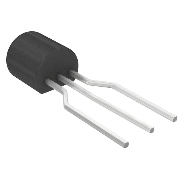
TO-92
Absolute Maximum Ratings
Symbol
VDSS
ID
{
S
SSN Series
GDS
TC = 25°C unless otherwise noted
Parameter
Drain-Source Voltage
- Continuous (TC = 25°C)
Drain Current
SSN1N45B
450
- Continuous (TC = 100°C)
IDM
Drain Current
VGSS
Gate-Source Voltage
EAS
Single Pulsed Avalanche Energy
IAR
Avalanche Current
EAR
Repetitive Avalanche Energy
Peak Diode Recovery dv/dt
Power Dissipation (TA = 25°C)
dv/dt
PD
- Pulsed
TL
Units
V
0.5
A
0.32
A
4.0
A
± 50
V
(Note 2)
108
mJ
(Note 1)
0.5
A
(Note 1)
0.25
5.5
0.9
mJ
V/ns
W
2.5
0.02
-55 to +150
W
W/°C
°C
300
°C
(Note 1)
(Note 3)
Power Dissipation (TL = 25°C)
TJ, Tstg
̵
̻
̻
- Derate above 25°C
Operating and Storage Temperature Range
Maximum lead temperature for soldering purposes,
1/8IGfrom case for 5 seconds
Thermal Characteristics
Symbol
RθJL
Parameter
Thermal Resistance, Junction-to-Lead
(Note 6a)
Typ
--
Max
50
Units
°C/W
RθJA
Thermal Resistance, Junction-to-Ambient
(Note 6b)
--
140
°C/W
©2002 Fairchild Semiconductor Corporation
Rev. A, November 2002
�Symbol
TC = 25°C unless otherwise noted
Parameter
Test Conditions
Min
Typ
Max
Units
450
--
--
V
--
0.5
--
V/°C
VDS = 450 V, VGS = 0 V
--
--
10
μA
VDS = 360 V, TC = 125°C
--
--
100
μA
Gate-Body Leakage Current, Forward
VGS = 50 V, VDS = 0 V
--
--
100
nA
Gate-Body Leakage Current, Reverse
VGS = -50 V, VDS = 0 V
--
--
-100
nA
VDS = VGS, ID = 250 μA
2.3
3.0
3.7
V
VDS = VGS, ID = 250 mA
3.5
4.2
4.9
V
Off Characteristics
BVDSS
Drain-Source Breakdown Voltage
VGS = 0 V, ID = 250 μA
ΔBVDSS
/
ΔTJ
Breakdown Voltage Temperature
Coefficient
ID = 250 μA, Referenced to 25°C
IDSS
IGSSF
IGSSR
Zero Gate Voltage Drain Current
On Characteristics
VGS(th)
Gate Threshold Voltage
RDS(on)
Static Drain-Source
On-Resistance
VGS = 10 V, ID = 0.25 A
--
3.4
4.25
Ω
gFS
Forward Transconductance
VDS = 50 V, ID = 0.25 A
--
0.7
--
S
VDS = 25 V, VGS = 0 V,
f = 1.0 MHz
--
185
240
pF
--
29
40
pF
--
6.5
8.5
pF
--
7.5
25
ns
--
21
50
ns
Dynamic Characteristics
Ciss
Input Capacitance
Coss
Output Capacitance
Crss
Reverse Transfer Capacitance
Switching Characteristics
td(on)
Turn-On Delay Time
tr
Turn-On Rise Time
td(off)
Turn-Off Delay Time
tf
Turn-Off Fall Time
Qg
Total Gate Charge
Qgs
Gate-Source Charge
Qgd
Gate-Drain Charge
VDD = 225 V, ID = 0.5 A,
RG = 25 Ω
(Note 4,5)
VDS = 360 V, ID = 0.5 A,
VGS = 10 V
(Note 4,5)
--
23
55
ns
--
36
80
ns
--
6.5
8.5
nC
--
0.9
--
nC
--
3.2
--
nC
Drain-Source Diode Characteristics and Maximum Ratings
IS
Maximum Continuous Drain-Source Diode Forward Current
--
--
0.5
A
ISM
--
--
4.0
A
VSD
Maximum Pulsed Drain-Source Diode Forward Current
VGS = 0 V, IS = 0.5 A
Drain-Source Diode Forward Voltage
--
--
1.4
V
trr
Reverse Recovery Time
--
102
--
ns
Qrr
Reverse Recovery Charge
VGS = 0 V, IS = 0.5 A,
dIF / dt = 100 A/μs
--
0.26
--
μC
(Note 4)
Notes:
1. Repetitive Rating : Pulse width limited by maximum junction temperature
2. L = 75mH, IAS = 1.6A, VDD = 50V, RG = 25 Ω, Starting TJ = 25°C
3. ISD ˺ 0.5A, di/dt ˺ 300A/μs, VDD ˺ BVDSS, Starting TJ = 25°C
4. Pulse Test : Pulse width ˺ 300μs, Duty cycle ˺ 2%
5. Essentially independent of operating temperature
6. a) Reference point of the RθJL is the drain lead
b) When mounted on 3”x4.5” FR-4 PCB without any pad copper in a still air environment
(RθJA is the sum of the junction-to-case and case-to-ambient thermal resistance. RθCA is determined by the user’s board design)
©2002 Fairchild Semiconductor Corporation
Rev. A, November 2002
SSN1N45B
Electrical Characteristics
�SSN1N45B
Typical Characteristics
VGS
15.0 V
10.0 V
8.0 V
6.0 V
5.5 V
5.0 V
Bottom : 4.5 V
0
ID, Drain Current [A]
10
ID , Drain Current [A]
Top :
-1
10
0
150ඓ
10
25ඓ
-55ඓ
ජ Notes :
1. 250த s Pulse Test
2. TC = 25ඓ
ජ Notes :
1. VDS = 50V
2. 250த s Pulse Test
-1
-1
0
10
10
1
10
10
2
4
6
8
10
VGS , Gate-Source Voltage [V]
VDS, Drain-Source Voltage [V]
Figure 1. On-Region Characteristics
Figure 2. Transfer Characteristics
12
IDR, Reverse Drain Current [A]
RDS(ON) [ ],
Drain-Source On-Resistance
10
VGS = 10V
8
VGS = 20V
6
4
2
0
10
150ඓ
25ඓ
ජ Notes :
1. VGS = 0V
2. 250த s Pulse Test
ජ Note : TJ = 25ඓ
-1
0
0
1
2
3
4
5
10
0.2
0.4
0.6
1.0
1.2
1.4
VSD, Source-Drain voltage [V]
Figure 3. On-Resistance Variation vs.
Drain Current and Gate Voltage
Figure 4. Body Diode Forward Voltage
Variation with Source Current
and Temperature
400
Ciss = Cgs + Cgd (Cds = shorted)
Coss = Cds + Cgd
Crss = Cgd
12
VDS = 90V
10
VDS = 225V
Ciss
200
Coss
100
Crss
ජ Note ;
1. VGS = 0 V
2. f = 1 MHz
VGS, Gate-Source Voltage [V]
300
Capacitance [pF]
0.8
ID, Drain Current [A]
VDS = 360V
8
6
4
2
ජ Note : ID = 0.5 A
0
-1
10
0
10
1
10
VDS, Drain-Source Voltage [V]
Figure 5. Capacitance Characteristics
©2002 Fairchild Semiconductor Corporation
0
0
1
2
3
4
5
6
7
QG, Total Gate Charge [nC]
Figure 6. Gate Charge Characteristics
Rev. A, November 2002
�SSN1N45B
Typical Characteristics
(Continued)
3.0
1.2
RDS(ON) , (Normalized)
Drain-Source On-Resistance
BV DSS , (Normalized)
Drain-Source Breakdown Voltage
2.5
1.1
1.0
ජ Notes :
1. VGS = 0 V
2. ID = 250 த A
0.9
0.8
-100
-50
0
50
100
150
2.0
1.5
1.0
ජ Notes :
1. VGS = 10 V
2. ID = 0.25 A
0.5
0.0
-100
200
-50
0
o
50
100
150
200
o
TJ, Junction Temperature [ C]
TJ, Junction Temperature [ C]
Figure 7. Breakdown Voltage Variation
vs. Temperature
Figure 8. On-Resistance Variation
vs. Temperature
0.6
Operation in This Area
is Limited by R DS(on)
1
0.5
100 μs
1 ms
10 ms
100 ms
1s
0
10
0.4
ID, Drain Current [A]
ID, Drain Current [A]
10
0.3
-1
10
DC
0.2
ජ Notes :
o
-2
1. TC = 25 C
10
o
2. TJ = 150 C
3. Single Pulse
0.1
-3
10
0
1
10
2
10
0.0
25
3
10
10
50
75
2
10
1
125
150
Figure 10. Maximum Drain Current
vs. Case Temperature
D = 0 .5
0 .2
0 .1
PDM
0 .0 5
10
t1
0 .0 2
0
t2
0 .0 1
θJ L
Z (t), T h e rm a l R e s p o n s e
Figure 9. Maximum Safe Operating Area
10
100
TC, Case Temperature [ඓ]
VDS, Drain-Source Voltage [V]
10
ජ N o te s :
1 . Z J L (t) = 5 0 ඓ /W M a x .
2 . D u ty F a c to r, D = t 1 /t 2
3 . T J M - T L = P D M * Z J L (t)
s i n g l e p u ls e
-1
10
-5
10
-4
10
-3
10
-2
10
-1
10
0
10
1
10
2
10
3
t 1 , S q u a r e W a v e P u ls e D u ra tio n [s e c ]
Figure 11. Transient Thermal Response Curve
©2002 Fairchild Semiconductor Corporation
Rev. A, November 2002
�SSN1N45B
Gate Charge Test Circuit & Waveform
VGS
Same Type
as DUT
50KԽ
Qg
200nF
12V
10V
300nF
VDS
VGS
Qgs
Qgd
DUT
3mA
Charge
Resistive Switching Test Circuit & Waveforms
VDS
RL
VDS
90%
VDD
VGS
RG
VGS
DUT
10V
10%
td(on)
tr
td(off)
t on
tf
t off
Unclamped Inductive Switching Test Circuit & Waveforms
BVDSS
1
EAS = ---- L IAS2 -------------------2
BVDSS - VDD
L
VDS
BVDSS
IAS
ID
RG
VDD
DUT
10V
tp
©2002 Fairchild Semiconductor Corporation
ID (t)
VDS (t)
VDD
tp
Time
Rev. A, November 2002
�SSN1N45B
Peak Diode Recovery dv/dt Test Circuit & Waveforms
DUT
+
VDS
_
I SD
L
Driver
RG
VGS
VGS
( Driver )
Same Type
as DUT
VDD
• dv/dt controlled by RG
• ISD controlled by pulse period
Gate Pulse Width
D = -------------------------Gate Pulse Period
10V
IFM , Body Diode Forward Current
I SD
( DUT )
di/dt
IRM
Body Diode Reverse Current
VDS
( DUT )
Body Diode Recovery dv/dt
VSD
VDD
Body Diode
Forward Voltage Drop
©2002 Fairchild Semiconductor Corporation
Rev. A, November 2002
�SSN1N45B
Package Dimensions
TO-92
+0.25
4.58 ±0.20
4.58 –0.15
±0.10
14.47 ±0.40
0.46
1.27TYP
[1.27 ±0.20]
1.27TYP
[1.27 ±0.20]
±0.20
(0.25)
+0.10
0.38 –0.05
1.02 ±0.10
3.86MAX
3.60
+0.10
0.38 –0.05
(R2.29)
Dimensions in Millimeters
©2002 Fairchild Semiconductor Corporation
Rev. A, November 2002
�TRADEMARKS
The following are registered and unregistered trademarks Fairchild Semiconductor owns or is authorized to use and is not
intended to be an exhaustive list of all such trademarks.
ACEx™
FACT™
FACT Quiet series™
ActiveArray™
FAST®
Bottomless™
FASTr™
CoolFET™
CROSSVOLT™ FRFET™
GlobalOptoisolator™
DOME™
GTO™
EcoSPARK™
HiSeC™
E2CMOS™
EnSigna™
I2C™
Across the board. Around the world.™
The Power Franchise™
Programmable Active Droop™
ImpliedDisconnect™
ISOPLANAR™
LittleFET™
MicroFET™
MicroPak™
MICROWIRE™
MSX™
MSXPro™
OCX™
OCXPro™
OPTOLOGIC®
OPTOPLANAR™
PACMAN™
POP™
Power247™
PowerTrench®
QFET™
QS™
QT Optoelectronics™
Quiet Series™
RapidConfigure™
RapidConnect™
SILENT SWITCHER®
SMART START™
SPM™
Stealth™
SuperSOT™-3
SuperSOT™-6
SuperSOT™-8
SyncFET™
TinyLogic™
TruTranslation™
UHC™
UltraFET®
VCX™
DISCLAIMER
FAIRCHILD SEMICONDUCTOR RESERVES THE RIGHT TO MAKE CHANGES WITHOUT FURTHER NOTICE TO ANY
PRODUCTS HEREIN TO IMPROVE RELIABILITY, FUNCTION OR DESIGN. FAIRCHILD DOES NOT ASSUME ANY
LIABILITY ARISING OUT OF THE APPLICATION OR USE OF ANY PRODUCT OR CIRCUIT DESCRIBED HEREIN;
NEITHER DOES IT CONVEY ANY LICENSE UNDER ITS PATENT RIGHTS, NOR THE RIGHTS OF OTHERS.
LIFE SUPPORT POLICY
FAIRCHILD’S PRODUCTS ARE NOT AUTHORIZED FOR USE AS CRITICAL COMPONENTS IN LIFE SUPPORT
DEVICES OR SYSTEMS WITHOUT THE EXPRESS WRITTEN APPROVAL OF FAIRCHILD SEMICONDUCTOR
CORPORATION.
As used herein:
1. Life support devices or systems are devices or systems
2. A critical component is any component of a life support
which, (a) are intended for surgical implant into the body,
device or system whose failure to perform can be
or (b) support or sustain life, or (c) whose failure to perform
reasonably expected to cause the failure of the life support
when properly used in accordance with instructions for use
device or system, or to affect its safety or effectiveness.
provided in the labeling, can be reasonably expected to
result in significant injury to the user.
PRODUCT STATUS DEFINITIONS
Definition of Terms
Datasheet Identification
Product Status
Definition
Advance Information
Formative or In
Design
This datasheet contains the design specifications for
product development. Specifications may change in
any manner without notice.
Preliminary
First Production
This datasheet contains preliminary data, and
supplementary data will be published at a later date.
Fairchild Semiconductor reserves the right to make
changes at any time without notice in order to improve
design.
No Identification Needed
Full Production
This datasheet contains final specifications. Fairchild
Semiconductor reserves the right to make changes at
any time without notice in order to improve design.
Obsolete
Not In Production
This datasheet contains specifications on a product
that has been discontinued by Fairchild semiconductor.
The datasheet is printed for reference information only.
©2002 Fairchild Semiconductor Corporation
Rev. I1
�Product
Product status
Pb-free Status
0.5A, 450V, RDS(on) = 4.25:@VGS = 10 V
Low gate charge (typical 6.5 nC)
Low Crss (typical 6.5 pF)
100% avalanche tested
Improved dv/dt capability
Gate-Source Voltage ± 50V guaranteed
back to top
Product status/pricing/packaging
z
z
z
z
z
z
Features
back to top
Pricing*
Package type
Leads
This advanced technology has been especially tailored to minimize on-state
resistance, provide superior switching performance, and withstand high
This page
energy pulse in the avalanche and commutation mode. These devices are
Print version
well suited for electronic ballasts based on half bridge configuration.
e-mail this datasheet
COMPANY
INVESTORS
Package Marking Convention**
Design center
Quality and reliability
Sales support
Support
Product Change Notices
(PCNs)
How to order products
Request samples
Related Links
SUPPORT
Packing method
DESIGN CENTER
Datasheet
Download this
datasheet
APPLICATIONS
These N-Channel enhancement mode power field effect transistors are
produced using Fairchild’s proprietary, planar, DMOS technology.
General description
•Qualification Support
TECHNICAL INFORMATION
Contents
•General description
•Features
•Product status/pricing/packaging
•Order Samples
450V N-Channel B-FET
SSN1N45B
Home >> Find products >>
DATASHEETS, SAMPLES, BUY
Go
Careers
MY FA
| Sitema
�Full Production
SSN1N45BTA
$0.394
$0.466
TO-92
TO-92
3
3
AMMO
BULK
Line 1: 1N45B Line 2: 3
Line 1: 1N45B Line 2: 3
Products | Design Center | Support | Company News | Investors | My Fairchild | Contact Us | Site Index | Privacy Policy | Site Terms & Conditions | Standard Terms & Conditions o
© 2007 Fairchild Semiconductor
back to top
SSN1N45BTA
SSN1N45BBU
Product
Click on a product for detailed qualification data
Qualification Support
back to top
Package marking information for product SSN1N45B is available. Click here for more information .
Indicates product with Pb-free second-level interconnect. For more information click here.
* Fairchild 1,000 piece Budgetary Pricing
** A sample button will appear if the part is available through Fairchild's on-line samples program. If there is no sample button, please
contact a Fairchild distributor to obtain samples
Full Production
SSN1N45BBU
�