843002
Femtoclock® Crystal-to-3.3V LVPECL
Frequency Synthesizer
Data Sheet
GENERAL DESCRIPTION
FEATURES
The 843002 is a two output LVPECL synthesizer optimized to
generate Fibre Channel reference clock frequencies . Using
a 26.5625MHz, 18pF parallel resonant crystal, the following
frequencies can be generated based on the 2 frequency select pins
(F_SEL[1:0]): 212.5MHz, 187.5MHz, 159.375MHz, 106.25MHz,
and 53.125MHz. The 843002 uses IDT’s 3rd generation low phase
noise VCO technology and can achieve 1ps or lower typical rms
phase jitter, easily meeting Fibre Channel jitter requirements. The
843002 is packaged in a small 20-pin TSSOP package.
• Two 3.3V LVPECL outputs
• Selectable crystal oscillator interface
or LVCMOS/LVTTL single-ended input
• Supports the following output frequencies: 212.5MHz,
187.5MHz, 159.375MHz, 106.25MHz and 53.125MHz
• VCO range: 560MHz - 680MHz
• RMS phase jitter (637kHz - 10MHz): 0.72ps (typical)
• Typical phase noise at 212.5MHz
Phase noise:
Offset
Noise Power
100Hz ................-87.7 dBc/Hz
1KHz ..............-111.6 dBc/Hz
10KHz ..............-124.3 dBc/Hz
100KHz ..............-124.3 dBc/Hz
• Full 3.3V supply mode
• Lead-Free package RoHS compliant
• -30°C to 85°C ambient operating temperature
FREQUENCY SELECT FUNCTION TABLE
PIN ASSIGNMENT
Inputs
Input Frequency
(MHz)
F_SEL1
F_SEL0
M Divider
Value
N Divider
Value
M/N
Divider Value
Output
Frequency
(MHz)
26.5625
0
0
24
3
8
212.5
26.5625
0
1
24
4
6
159.375
26.5625
1
0
24
6
4
106.25
26.5625
1
1
24
12
2
53.125
23.4375
0
0
24
3
8
187.5
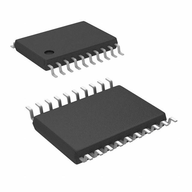
843002
20-Lead TSSOP
6.5mm x 4.4mm x 0.92mm
package body
G Package
Top View
BLOCK DIAGRAM
F_SEL[1:0] Pulldown
2
nPLL_SEL Pulldown
Q0
F_SEL[1:0]
TEST_CLK Pulldown
1
00
01
10
11
1
26.5625MHz
XTAL_IN
OSC
0
Phase
Detector
XTAL_OUT
VCO
637.5MHz
(w/26.5625MHz
Reference)
0
÷3
÷4
÷6
÷12
nQ0
Q1
nQ1
nXTAL_SEL Pulldown
M = 24 (fixed)
MR Pulldown
©2016 Integrated Device Technology, Inc
1
Revision B January 21, 2016
�843002 Data Sheet
TABLE 1. PIN DESCRIPTIONS
Number
Name
1, 7
nc
Type
2, 20
VCCO
Power
3, 4
Q0, nQ0
Ouput
Unused
Description
No connect.
Output supply pins.
Differential output pair. LVPECL interface levels.
Active HIGH Master Reset. When logic HIGH, the internal dividers are reset
causing the true outputs Qx to go low and the inverted outputs nQx
Pulldown
to go high. When logic LOW, the internal dividers and the outputs are enabled. LVCMOS/LVTTL interface levels.
Selects between the PLL and TEST_CLK as input to the dividers. When
Pulldown LOW, selects PLL (PLL Enable). When HIGH, deselects the reference clock
(PLL Bypass). LVCMOS/LVTTL interface levels.
5
MR
Input
6
nPLL_SEL
Input
8
VCCA
Power
9, 11
F_SEL0,
F_SEL1
Input
10, 16
VCC
Power
Core supply pin.
12, 13
XTAL_OUT,
XTAL_IN
Input
Parallel resonant crystal interface. XTAL_OUT is the output,
XTAL_IN is the input.
14
TEST_CLK
Input
Pulldown LVCMOS/LVTTL clock input.
15
nXTAL_SEL
Input
Selects between crystal or TEST_CLK inputs as the the PLL Reference
Pulldown source. Selects XTAL inputs when LOW. Selects TEST_CLK when HIGH.
LVCMOS/LVTTL interface levels.
17
VEE
Power
Negative supply pins.
18, 19
nQ1, Q1
Output
Differential output pair. LVPECL interface levels.
Analog supply pin.
Pulldown Frequency select pins. LVCMOS/LVTTL interface levels.
NOTE: Pulldown refer to internal input resistors. See Table 2, Pin Characteristics, for typical values.
TABLE 2. PIN CHARACTERISTICS
Symbol
Parameter
CIN
Input Capacitance
4
pF
RPULLDOWN
Input Pulldown Resistor
51
kΩ
©2016 Integrated Device Technology, Inc
Test Conditions
2
Minimum
Typical
Maximum
Units
Revision B January 21, 2016
�843002 Data Sheet
ABSOLUTE MAXIMUM RATINGS
Supply Voltage, VCC
4.6V
Inputs, VI
-0.5V to VCC + 0.5V
Outputs, IO
Continuous Current
Surge Current
50mA
100mA
Package Thermal Impedance, θJA
73.2°C/W (0 lfpm)
Storage Temperature, TSTG
-65°C to 150°C
NOTE: Stresses beyond those listed under Absolute
Maximum Ratings may cause permanent damage to the
device. These ratings are stress specifications only. Functional
operation of product at these conditions or any conditions
beyond those listed in the DC Characteristics or AC Characteristics is not implied. Exposure to absolute maximum rating
conditions for extended periods may affect product reliability.
TABLE 3A. POWER SUPPLY DC CHARACTERISTICS, VCC = VCCA = VCCO = 3.3V±10%, TA = -30°C TO 85°C
Symbol
Parameter
VCC
VCCA
Test Conditions
Minimum
Typical
Maximum
Units
Core Supply Voltage
2.97
3.3
3.63
V
Analog Supply Voltage
2.97
3.3
3.63
V
VCCO
Output Supply Voltage
2.97
3.3
3.63
V
IEE
Power Supply Current
135
mA
ICC
Core Supply Current
100
mA
ICCA
Analog Supply Current
15
mA
ICCO
Output Supply Current
31
mA
TABLE 3B. LVCMOS / LVTTL DC CHARACTERISTICS, VCC = VCCA = VCCO = 3.3V±10%, TA = -30°C TO 85°C
Symbol
Parameter
VIH
Input High Voltage
nPLL_SEL, nXTAL_SEL,
Input
F_SEL0, F_SEL1, MR
Low Voltage
TEST_CLK
TEST_CLK, MR,
Input
F_SEL0, F_SEL1,
High Current
nPLL_SEL, nXTAL_SEL,
TEST_CLK, MR,
Input
F_SEL0, F_SEL1,
Low Current
nPLL_SEL, nXTAL_SEL,
VIL
IIH
IIL
Test Conditions
Minimum
Typical
Maximum
Units
2
VCC + 0.3
V
-0.3
0.8
V
-0.3
1.0
V
150
µA
VCC = VIN = 3.63V
VCC = 3.63V, VIN = 0V
-150
µA
TABLE 3C. LVPECL DC CHARACTERISTICS, VCC = VCCA = VCCO = 3.3V±10%, TA = -30°C TO 85°C
Symbol
Parameter
Maximum
Units
VOH
Output High Voltage; NOTE 1
Test Conditions
Minimum
VCCO - 1.4
Typical
VCCO - 0.9
V
VOL
Output Low Voltage; NOTE 1
VCCO - 2.0
VCCO - 1.7
V
VSWING
Peak-to-Peak Output Voltage Swing
0.6
1.0
V
NOTE 1: Outputs terminated with 50Ω to VCCO - 2V.
©2016 Integrated Device Technology, Inc
3
Revision B January 21, 2016
�843002 Data Sheet
TABLE 4. CRYSTAL CHARACTERISTICS
Parameter
Test Conditions
Minimum
Maximum
Units
28.33
MHz
Equivalent Series Resistance (ESR)
50
Ω
Shunt Capacitance
7
pF
Maximum
Units
Mode of Oscillation
Typical
Fundamental
Frequency
23.33
26.5625
NOTE: Characterized using an 18pF parallel resonant crystal.
TABLE 5. AC CHARACTERISTICS, VCC = VCCA = VCCO = 3.3V±10%, TA = -30°C TO 85°C
Symbol
fOUT
tsk(o)
Parameter
Output Frequency
Test Conditions
Minimum
Typical
F_SEL[1:0] = 00
186.67
226.67
MHz
F_SEL[1:0] = 01
140
170
MHz
F_SEL[1:0] = 10
93.33
113.33
MHz
F_SEL[1:0] =11
46.67
56.67
MHz
20
ps
Output Skew; NOTE 1, 2
tjit(Ø)
RMS Phase Jitter (Random);
NOTE 3
tR / tF
Output Rise/Fall Time
odc
Output Duty Cycle
212.5MHz, (637KHz - 10MHz)
0.72
ps
159.375MHz, (637KHz - 10MHz)
0.76
ps
106.25MHz, (637KHz - 10MHz)
0.84
ps
53.125MHz, (637KHz - 10MHz)
0.97
300
600
ps
F_SEL[1:0] =00
46
54
%
51
%
F_SEL[1:0] ¹ 00
49
NOTE 1: Defined as skew between outputs at the same supply voltages and with equal load conditions.
Measured at VCCO/2.
NOTE 2: This parameter is defined in accordance with JEDEC Standard 65.
NOTE 3: See Phase Noise plot.
©2016 Integrated Device Technology, Inc
ps
20% to 80%
4
Revision B January 21, 2016
�843002 Data Sheet
TYPICAL PHASE NOISE AT 53.125MHZ
0
-10
-20
-30
53.125MHz
-40
RMS Phase Jitter (Random)
637Khz to 10MHz = 0.97ps (typical)
➤
-50
-70
Fibre Channel Jitter Filter
-80
-90
Raw Phase Noise Data
-100
-110
➤
NOISE POWER dBc
Hz
-60
-120
-130
-140
-150
-160
-190
➤
-170
-180
10
100
1k
Phase Noise Result by adding
Fibre Channel Filter to raw data
10k
100k
1M
10M
100M
OFFSET FREQUENCY (HZ)
TYPICAL PHASE NOISE AT 106.25MHZ
0
-10
-20
-30
106.25MHz
-40
RMS Phase Jitter (Random)
637Khz to 10MHz = 0.84ps (typical)
➤
-50
-70
Fibre Channel Jitter Filter
-80
-90
Raw Phase Noise Data
-100
➤
NOISE POWER dBc
Hz
-60
-110
-120
-130
-140
➤
-150
-160
-170
-180
-190
10
100
1k
10k
Phase Noise Result by adding
Fibre Channel Filter to raw data
100k
1M
10M
100M
OFFSET FREQUENCY (HZ)
©2016 Integrated Device Technology, Inc
5
Revision B January 21, 2016
�843002 Data Sheet
TYPICAL PHASE NOISE AT 159.375MHZ
0
-10
-20
-30
159.375MHz
-40
RMS Phase Jitter (Random)
637Khz to 10MHz = 0.76ps (typical)
➤
-50
-70
Fibre Channel Jitter Filter
-80
-90
Raw Phase Noise Data
-100
➤
NOISE POWER dBc
Hz
-60
-110
-120
-130
-140
➤
-150
-160
-170
-180
-190
Phase Noise Result by adding
Fibre Channel Filter to raw data
10
100
1k
10k
100k
1M
10M
100M
OFFSET FREQUENCY (HZ)
TYPICAL PHASE NOISE AT 212.5MHZ
0
-10
-20
-30
212.5MHz
-40
RMS Phase Jitter (Random)
637Khz to 10MHz = 0.72ps (typical)
➤
-50
Fibre Channel Jitter Filter
-70
-80
Raw Phase Noise Data
-90
-100
➤
NOISE POWER dBc
Hz
-60
-110
-120
-130
-140
➤
-150
-160
-170
-180
Phase Noise Result by adding
Fibre Channel Filter to raw data
-190
10
100
1k
10k
100k
1M
10M
100M
OFFSET FREQUENCY (HZ)
©2016 Integrated Device Technology, Inc
6
Revision B January 21, 2016
�843002 Data Sheet
PARAMETER MEASUREMENT INFORMATION
3.3V CORE/3.3V OUTPUT LOAD TEST CIRCUIT
OUTPUT SKEW
RMS PHASE JITTER
OUTPUT RISE/FALL TIME
OUTPUT DUTY CYCLE/PULSE WIDTH/PERIOD
©2016 Integrated Device Technology, Inc
7
Revision B January 21, 2016
�843002 Data Sheet
APPLICATIONS INFORMATION
POWER SUPPLY FILTERING TECHNIQUES
As in any high speed analog circuitry, the power supply
pins are vulnerable to random noise. The 843002 provides
separate power supplies to isolate any high switching
noise from the outputs to the internal PLL. VCC, VCCA, and
VCCO should be individually connected to the power supply
plane through vias, and bypass capacitors should be
used for each pin. To achieve optimum jitter performance,
power supply isolation is required. Figure 1 illustrates how
a 10Ω resistor along with a 10µF and a .01μF bypass
capacitor should be connected to each VCCA.
3.3V
VCC
.01μF
10Ω
VCCA
.01μF
10μF
FIGURE 1. POWER SUPPLY FILTERING
TERMINATION FOR 3.3V LVPECL OUTPUT
The clock layout topology shown below is a typical termination
for LVPECL outputs. The two different layouts mentioned are
recommended only as guidelines.
drive 50Ω transmission lines. Matched impedance techniques
should be used to maximize operating frequency and minimize
signal distortion. Figures 2A and 2B show two different layouts
which are recommended only as guidelines. Other suitable clock
layouts may exist and it would be recommended that the board
designers simulate to guarantee compatibility across all printed
circuit and clock component process variations.
Differential outputs are low impedance follower outputs that
generate ECL/LVPECL compatible outputs. Therefore, terminating resistors (DC current path to ground) or current sources
must be used for functionality. These outputs are designed to
FIGURE 2A. LVPECL OUTPUT TERMINATION
©2016 Integrated Device Technology, Inc
FIGURE 2B. LVPECL OUTPUT TERMINATION
8
Revision B January 21, 2016
�843002 Data Sheet
CRYSTAL INPUT INTERFACE
The 843002 has been characterized with 18pF parallel resonant
crystals. The capacitor values shown in Figure 3 below were
determined using a 26.5625MHz 18pF parallel resonant crystal
and were chosen to minimize the ppm error.
Figure 3. CRYSTAL INPUt INTERFACE
©2016 Integrated Device Technology, Inc
9
Revision B January 21, 2016
�843002 Data Sheet
LAYOUT GUIDELINE
pF parallel resonant 26.5625MHz crystal is used. The C1=27pF
and C2=33pF are recommended for frequency accuracy. For
different board layout, the C1 and C2 may be slightly adjusted
for optimizing frequency accuracy.
Figure 4A shows a schematic example of the 843002. An
example of LVEPCL termination is shown in this schematic.
Additional LVPECL termination approaches are shown in the
LVPECL Termination Application Note. In this example, an 18
Zo = 50 Ohm
VCCA
VCC
R2
10
C3
10uF
+
Zo = 50 Ohm
C4
0.01u
-
VCC
VCCO
C6
0.1u
Set Logic
Input to
'0'
VCC
VCCO=3.3V
Zo = 50 Ohm
+
11
12
13
14
15
16
17
18
19
20
RD1
Not Install
F_SEL1
XTAL_OUT
XTAL_IN
TEST_CLK
nXTAL_SEL
VCC
VEE
nQ1
Q1
VCCO
To Logic
Input
pins
To Logic
Input
pins
R5
50
ICS843002
VCC=3.3V
RU2
Not Install
RU1
1K
R6
50
U1
VCC
F_SEL0
VCCA
nc
nPLL_SEL
MR
nQ0
Q0
VCCO
nc
Set Logic
Input to
'1'
VCC
R4
50
C7
0.1u
10
9
8
7
6
5
4
3
2
1
Logic Control Input Examples
RD2
1K
Zo = 50 Ohm
VCCO
C8
0.1u
R8
50
C2
33pF
X1
18pF
VCC
R7
50
26.5625 MHz
C1
27pF
R9
50
C9
0.1u
FIGURE 4A. 843002 SCHEMATIC EXAMPLE
PC BOARD LAYOUT EXAMPLE
Figure 4B shows an example of 843002 P.C. board layout. The
crystal X1 footprint shown in this example allows installation of
either surface mount HC49S or through-hole HC49 package.
The footprints of other components in this example are listed in
the Table 6. There should be at least one decoupling capacitor
per power pin. The decoupling capacitors should be located as
close as possible to the power pins. The layout assumes that the
board has clean analog power ground plane.
TABLE 6. FOOTPRINT TABLE
Reference
Size
C1, C2
0402
C3
C4, C5, C6, C7, C8
R2
0805
0603
0603
NOTE: Table 6, lists component sizes
shown in this layout example.
FIGURE 4B. 843002 PC BOARD LAYOUT EXAMPLE
©2016 Integrated Device Technology, Inc
10
Revision B January 21, 2016
�843002 Data Sheet
POWER CONSIDERATIONS
This section provides information on power dissipation and junction temperature for the 843002.
Equations and example calculations are also provided.
1. Power Dissipation.
The total power dissipation for the 843002 is the sum of the core power plus the power dissipated in the load(s).
The following is the power dissipation for VCC = 3.3V + 10% = 3.63V, which gives worst case results.
NOTE: Please refer to Section 3 for details on calculating power dissipated in the load.
•
•
Power (core)MAX = VCC_MAX * IEE_MAX = 3.63V * 135mA = 490mW
Power (outputs)MAX = 30mW/Loaded Output pair
If all outputs are loaded, the total power is 2 * 30mW = 60mW
Total Power_MAX (3.63V, with all outputs switching) = 490mW + 60mW = 550mW
2. Junction Temperature.
JJunction temperature at the junction of the bond wire and bond pad directly affects the reliability of the device. The maximum
recommended junction temperature is 125°C. Limiting the internal transistor junction temperature, Tj, to 125°C ensures that the
bond wire and bond pad temperature remains below 125°C.
The equation for Tj is as follows: Tj = θJA * Pd_total + TA
Tj = Junction Temperature
θJA = Junction-to-Ambient Thermal Resistance
Pd_total = Total Device Power Dissipation (example calculation is in section 1 above)
TA = Ambient Temperature
In order to calculate junction temperature, the appropriate junction-to-ambient thermal resistance θJA must be used. Assuming
a moderate air flow of 200 linear feet per minute and a multi-layer board, the appropriate value is 66.6°C/W per Table 7 below.
Therefore, Tj for an ambient temperature of 85°C with all outputs switching is:
85°C + 0.550W * 66.6°C/W = 121.6°C. This is below the limit of 125°C.
This calculation is only an example. Tj will obviously vary depending on the number of loaded outputs, supply voltage, air flow,
and the type of board (single layer or multi-layer).
TABLE 7. THERMAL RESISTANCE θJA FOR 20-PIN TSSOP, FORCED CONVECTION
θJA by Velocity (Linear Feet per Minute)
Single-Layer PCB, JEDEC Standard Test Boards
Multi-Layer PCB, JEDEC Standard Test Boards
0
200
114.5°C/W
73.2°C/W
98.0°C/W
66.6°C/W
500
88.0°C/W
63.5°C/W
NOTE: Most modern PCB designs use multi-layered boards. The data in the second row pertains to most designs.
©2016 Integrated Device Technology, Inc
11
Revision B January 21, 2016
�843002 Data Sheet
3. Calculations and Equations.
The purpose of this section is to derive the power dissipated into the load.
LVPECL output driver circuit and termination are shown in Figure 5.
FIGURE 5. LVPECL DRIVER CIRCUIT AND TERMINATION
To calculate worst case power dissipation into the load, use the following equations which assume a 50Ω load, and a termination
voltage of VCCO- 2V.
•
For logic high, VOUT = VOH_MAX = VCCO_MAX – 0.9V
(VCCO_MAX - VOH_MAX) = 0.9V
•
For logic low, VOUT = VOL_MAX = VCCO_MAX – 1.7V
(VCCO_MAX - VOL_MAX) = 1.7V
Pd_H is power dissipation when the output drives high.
Pd_L is the power dissipation when the output drives low.
Pd_H = [(VOH_MAX – (VCCO_MAX - 2V))/RL] * (VCCO_MAX - VOH_MAX) = [(2V - (VCCO_MAX - VOH_MAX))/RL] * (VCCO_MAX - VOH_MAX) =
[(2V - 0.9V)/50Ω] * 0.9V = 19.8mW
Pd_L = [(VOL_MAX – (VCCO_MAX - 2V))/RL] * (VCCO_MAX - VOL_MAX) = [(2V - (VCCO_MAX - VOL_MAX))/RL] * (VCCO_MAX - VOL_MAX) =
[(2V - 1.7V)/50Ω] * 1.7V = 10.2mW
Total Power Dissipation per output pair = Pd_H + Pd_L = 30mW
©2016 Integrated Device Technology, Inc
12
Revision B January 21, 2016
�843002 Data Sheet
RELIABILITY INFORMATION
TABLE 8. θJAVS. AIR FLOW TABLE FOR 20 LEAD TSSOP
θJA by Velocity (Linear Feet per Minute)
Single-Layer PCB, JEDEC Standard Test Boards
Multi-Layer PCB, JEDEC Standard Test Boards
0
200
500
114.5°C/W
73.2°C/W
98.0°C/W
66.6°C/W
88.0°C/W
63.5°C/W
NOTE: Most modern PCB designs use multi-layered boards. The data in the second row pertains to most designs.
TRANSISTOR COUNT
The transistor count for 843002 is: 2578
©2016 Integrated Device Technology, Inc
13
Revision B January 21, 2016
�843002 Data Sheet
PACKAGE OUTLINE - G SUFFIX FOR 20 LEAD TSSOP
TABLE 9. PACKAGE DIMENSIONS
Millimeters
SYMBOL
MIN
N
MAX
20
A
--
1.20
A1
0.05
0.15
A2
0.80
1.05
b
0.19
0.30
c
0.09
0.20
D
6.40
E
E1
6.60
6.40 BASIC
4.30
e
4.50
0.65 BASIC
L
0.45
0.75
α
0°
8°
aaa
--
0.10
Reference Document: JEDEC Publication 95, MO-153
©2016 Integrated Device Technology, Inc
14
Revision B January 21, 2016
�843002 Data Sheet
TABLE 10. ORDERING INFORMATION
Part/Order Number
Marking
Package
Shipping Packaging
Temperature
843002AGLF
ICS843002AGL
20 Lead “Lead-Free” TSSOP
tube
-30°C to 85°C
843002AGLFT
ICS843002AGL
20 Lead “Lead-Free” TSSOP
tape & reel
-30°C to 85°C
©2016 Integrated Device Technology, Inc
15
Revision B January 21, 2016
�843002 Data Sheet
REVISION HISTORY SHEET
Rev
Table
A
Page
1
Description of Change
Date
Added 187.5MHz to the Frequency Selection Function Table.
8/26/04
A
T10
15
Ordering Information Table - added Lead Free part number.
9/30/04
A
T5
4
AC Characteristics Table - corrected typo, fOUT 180.67 min. to 186.67 min.
12/27/04
1
Features section - corrected frequency bullet to read “Supports...output frequencies...” from “...input frequencies...”.
Ordering Information Table - updated table.
2/7/05
A
B
B
B
T10
15
T5
4
AC Characteristics Table - deleted Propagation Delay.
5/6/05
T10
14
Ordering Information Table - corrected lead-free marking.
Updated Datasheet Header and Footer.
4/17/13
T10
1
15
Deleted ICS from part numbers where needed.
Corrected part number in the header.
Ordering Information - Corrected Package information from 8 Lead TSSOP to 20
Lead TSSOP. Added T to tape and reel part number.
Updated header and footer.
1/21/16
©2016 Integrated Device Technology, Inc
16
Revision B January 21, 2016
�843002 Data Sheet
Corporate Headquarters
6024 Silver Creek Valley Road
San Jose, CA 95138 USA
www.IDT.com
Sales
1-800-345-7015 or 408-284-8200
Fax: 408-284-2775
www.IDT.com/go/sales
Tech Support
www.idt.com/go/support
DISCLAIMER Integrated Device Technology, Inc. (IDT) reserves the right to modify the products and/or specifications described herein at any time, without notice, at IDT's sole discretion. Performance specifications and
operating parameters of the described products are determined in an independent state and are not guaranteed to perform the same way when installed in customer products. The information contained herein is provided
without representation or warranty of any kind, whether express or implied, including, but not limited to, the suitability of IDT's products for any particular purpose, an implied warranty of merchantability, or non-infringement of the intellectual property rights of others. This document is presented only as a guide and does not convey any license under intellectual property rights of IDT or any third parties.
IDT's products are not intended for use in applications involving extreme environmental conditions or in life support systems or similar devices where the failure or malfunction of an IDT product can be reasonably expected to significantly affect the health or safety of users. Anyone using an IDT product in such a manner does so at their own risk, absent an express, written agreement by IDT.
Integrated Device Technology, IDT and the IDT logo are trademarks or registered trademarks of IDT and its subsidiaries in the United States and other countries. Other trademarks used herein are the property of IDT or
their respective third party owners.
For datasheet type definitions and a glossary of common terms, visit www.idt.com/go/glossary.
Copyright ©2016 Integrated Device Technology, Inc. All rights reserved.
�IMPORTANT NOTICE AND DISCLAIMER
RENESAS ELECTRONICS CORPORATION AND ITS SUBSIDIARIES (“RENESAS”) PROVIDES TECHNICAL
SPECIFICATIONS AND RELIABILITY DATA (INCLUDING DATASHEETS), DESIGN RESOURCES (INCLUDING
REFERENCE DESIGNS), APPLICATION OR OTHER DESIGN ADVICE, WEB TOOLS, SAFETY INFORMATION, AND
OTHER RESOURCES “AS IS” AND WITH ALL FAULTS, AND DISCLAIMS ALL WARRANTIES, EXPRESS OR IMPLIED,
INCLUDING, WITHOUT LIMITATION, ANY IMPLIED WARRANTIES OF MERCHANTABILITY, FITNESS FOR A
PARTICULAR PURPOSE, OR NON-INFRINGEMENT OF THIRD PARTY INTELLECTUAL PROPERTY RIGHTS.
These resources are intended for developers skilled in the art designing with Renesas products. You are solely responsible
for (1) selecting the appropriate products for your application, (2) designing, validating, and testing your application, and (3)
ensuring your application meets applicable standards, and any other safety, security, or other requirements. These
resources are subject to change without notice. Renesas grants you permission to use these resources only for
development of an application that uses Renesas products. Other reproduction or use of these resources is strictly
prohibited. No license is granted to any other Renesas intellectual property or to any third party intellectual property.
Renesas disclaims responsibility for, and you will fully indemnify Renesas and its representatives against, any claims,
damages, costs, losses, or liabilities arising out of your use of these resources. Renesas' products are provided only subject
to Renesas' Terms and Conditions of Sale or other applicable terms agreed to in writing. No use of any Renesas resources
expands or otherwise alters any applicable warranties or warranty disclaimers for these products.
(Rev.1.0 Mar 2020)
Corporate Headquarters
Contact Information
TOYOSU FORESIA, 3-2-24 Toyosu,
Koto-ku, Tokyo 135-0061, Japan
www.renesas.com
For further information on a product, technology, the most
up-to-date version of a document, or your nearest sales
office, please visit:
www.renesas.com/contact/
Trademarks
Renesas and the Renesas logo are trademarks of Renesas
Electronics Corporation. All trademarks and registered
trademarks are the property of their respective owners.
© 2020 Renesas Electronics Corporation. All rights reserved.
�


 工商网监
湘ICP备2023018690号
工商网监
湘ICP备2023018690号
