87972I
Low Skew, 1-to-12 LVCMOS/LVTTL
Clock Multiplier/Zero Delay Buffer
Data Sheet
GENERAL DESCRIPTION
FEATURES
The 87972I is a low skew, LVCMOS/LVTTL Clock Generator.
The 87972I has three selectable inputs and provides fourteen
LVCMOS/LVTTL outputs.
• Fully integrated PLL
The 87972I is a highly flexible device. Using the crystal
oscillator input, it can be used to generate clocks for a
system. All of these clocks can be the same frequency
or the device can be configured to generate up to three
different frequencies among the three output banks. Using one
of the single ended inputs, the 87972I can be used as a zero
delay buffer/multiplier/divider in clock distribution applications.
• Selectable crystal oscillator interface or LVCMOS/LVTTL
reference clock inputs
The three output banks and feedback output each have their
own output dividers which allows the device to generate a
multitude of different bank frequency ratios and output-to-input
frequency ratios. In addition, 2 outputs in Bank C (QC2, QC3)
can be selected to be inverting or non-inverting. The output
frequency range is 8.33MHz to125MHz. Input frequency range
is 5MHz to 120MHz.
• Output skew: 550ps (maximum)
The 87972I also has a QSYNC output which can be used
for system synchronization purposes. It monitors Bank A and
Bank C outputs and goes low one period of the faster clock
prior to coincident rising edges of Bank A and Bank C clocks.
QSYNC then goes high again when the coincident rising edges
of Bank A and Bank C occur. This feature is used primarily in
applications where Bank A and Bank C are running at different
frequencies, and is particularly useful when they are running at
non-integer multiples of one another.
• Compatible with PowerPC™ and Pentium™ Microprocessors
• Fourteen LVCMOS/LVTTL outputs; (12) clocks,
(1) feedback, (1) sync
• CLK0, CLK1 can accept the following input levels:
LVCMOS or LVTTL
• Output frequency range: 8.33MHz to 125MHz
• VCO range: 200MHz to 480MHz
• Cycle-to-cycle jitter: ±100ps (typical)
• Full 3.3V supply voltage
• -40°C to 85°C ambient operating temperature
• Available in lead-free RoHS-compliant package
PIN ASSIGNMENT
Example Applications:
1. System Clock generator: Use a 16.66MHz Crystal to
generate eight 33.33MHz copies for PCI and four
100MHz copies for the CPU or PCI-X.
2. Line Card Multiplier: Multiply 19.44MHz from a back
plane to 77.76MHz for the line Card ASICs and Serdes.
3. Zero Delay buffer for Synchronous memory: Fan out up
to twelve 100MHz copies from a memory controller reference clock to the memory chips on a memory module
with zero delay.
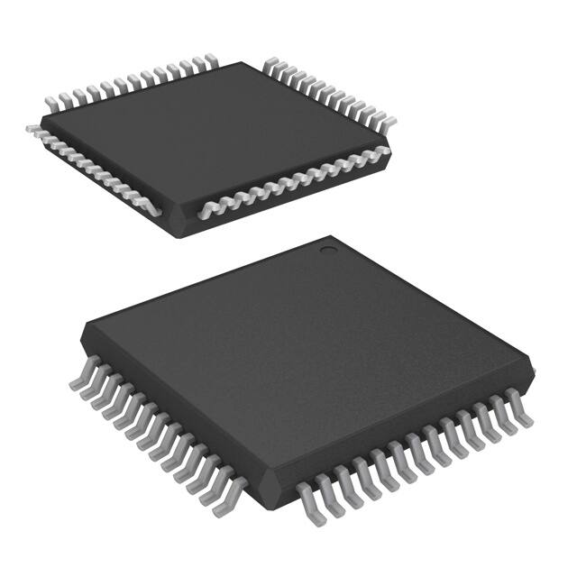
52-Lead LQFP
10mm x 10mm x 1.4mm package body
Y package
Top View
©2016 Integrated Device Technology, Inc
1
Revision E January 25, 2016
�87972I Data Sheet
BLOCK DIAGRAM
XTAL1
XTAL2
VCO_SEL
PLL_SEL
REF_SEL
1
D
0
CLK0
0
CLK1
1
Q
0
PHASE
DETECTOR
1
VCO
LPF
CLK_SEL
EXT_FB
D
Q
SYNC
FRZ
QA0
SYNC
FRZ
QA1
SYNC
FRZ
QA2
SYNC
FRZ
QA3
SYNC
FRZ
QB0
SYNC
FRZ
QB1
SYNC
FRZ
QB2
SYNC
FRZ
QB3
FSEL_FB2
D
nMR/OE
POWER-ON
RESET
Q
÷4, ÷6, ÷8, ÷12
÷4, ÷6, ÷8, ÷10
D
Q
÷2, ÷4, ÷6, ÷8
FSEL_A0:1
2
0
÷4, ÷6, ÷8, ÷10
÷2
2
D
Q
D
Q
QC0
SYNC
FRZ
QC1
SYNC
FRZ
QC2
SYNC
FRZ
QC3
QFB
1
FSEL_B0:1
FSEL_C0:1
2
SYNC PULSE
3
FSEL_FB0:2
SYNC
FRZ
QSYNC
DATA GENERATOR
FRZ_CLK
OUTPUT DISABLE
CIRCUITRY
12
FRZ_DATA
INV_CLK
©2016 Integrated Device Technology, Inc
2
Revision E January 25, 2016
�87972I Data Sheet
SIMPLIFIED BLOCK DIAGRAM
nMR/OE
FSEL_A[0:1]
XTAL1
2
XTAL2
CLK0
0
CLK1
1
1
0
CLK_SEL
PLL
VCO RANGE
200MHz - 480MHz
0
REF_SEL
÷2
QAx
÷4
÷6
÷8
÷12
0
EXT_FB
1
÷1
FSEL_
A1 A0
0 0
0 1
1 0
1 1
SYNC
FRZ
QA0
SYNC
FRZ
QA1
SYNC
FRZ
QA2
SYNC
FRZ
QA3
SYNC
FRZ
QB0
SYNC
FRZ
QB1
SYNC
FRZ
QB2
SYNC
FRZ
QB3
FSEL_B[0:1]
2
1
FSEL_
B1 B0
0 0
0 1
1 0
1 1
VCO_SEL
PLL_SEL
QBx
÷4
÷6
÷8
÷10
FSEL_C[0:1]
2
FSEL_
C1 C0
0 0
0 1
1 0
1 1
QCx
÷2
÷4
÷6
÷8
QC0
0
1
SYNC
FRZ
QC1
SYNC
FRZ
QC2
SYNC
FRZ
QC3
INV_CLK
FSEL_FB[0:2]
3
FRZ_CLK
FRZ_DATA
FSEL_
FB2 FB1 FB0 QFB
0
0
0
÷4
0
0
1
÷6
0
1
0
÷8
0
1
1 ÷10
1
0
0
÷8
1
0
1 ÷12
1
1
0 ÷16
1
1
1 ÷20
OUTPUT DISABLE
CIRCUITRY
©2016 Integrated Device Technology, Inc
3
QFB
SYNC
FRZ
QSYNC
Revision E January 25, 2016
�87972I Data Sheet
TABLE 1. PIN DESCRIPTIONS
Number
Name
1
GNDI
Type
Power
Description
Power supply ground.
2
nMR/OE
Input
Active HIGH Master Reset. Active LOW output enable. When logic HIGH,
the internal dividers are reset and the outputs are in high impedance
Pullup
(Hi-Z). When logic LOW, the internal dividers and the outputs are enabled.
LVCMOS / LVTTL interface levels.
3
FRZ_CLK
Input
Pullup Clock input for freeze circuitry. LVCMOS / LVTTL interface levels.
4
FRZ_DATA
Input
Pullup
Configuration data input for freeze circuitry.
LVCMOS / LVTTL interface levels.
5, 26, 27
FSEL_FB2,
FSEL_FB1,
FSEL_FB0
Input
Pullup
Select pins control Feedback Divide value.
LVCMOS / LVTTL interface levels.
6
PLL_SEL
Input
7
REF_SEL
Input
8
CLK_SEL
Input
9, 10
CLK0, CLK1
Input
11, 12
XTAL1, XTAL2
Input
Crystal oscillator interface. XTAL1 is the input. XTAL2 is the output.
13
VDDA
Power
Analog supply pin.
14
INV_CLK
Input
15, 24, 30,
35, 39, 47, 51
GNDO
Power
Power supply ground.
16, 18, 21, 23
QC3, QC2,
QC1, QC0
Output
Bank C clock outputs. 7Ω typical output impedance.
LVCMOS / LVTTL interface levels.
17, 22, 33
37, 45, 49
VDDO
Power
Output supply pins.
19, 20
FSEL_C1,
FSEL_C0
Input
25
QSYNC
Output
Synchronization output for Bank A and Bank C. Refer to Figure 1,
Timing Diagrams. LVCMOS / LVTTL interface levels.
28
VDD
Power
Core supply pins.
29
QFB
Output
Feedback clock output. LVCMOS / LVTTL interface levels.
EXT_FB
Input
31
32, 34, 36, 38
40, 41
42, 43
44, 46, 48, 50
52
QB3, QB2,
QB1, QB0
FSEL_B1,
FSEL_B0
FSEL_A1,
FSEL_A0
QA3, QA2,
QA1, QA0
VCO_SEL
Output
Selects between the PLL and reference clocks as the input to the output
Pullup dividers. When HIGH, selects PLL. When LOW, bypasses the PLL and
reference clocks. LVCMOS / LVTTL interface levels.
Selects between crystal and reference clock. When LOW, selects
Pullup CLK0 or CLK1. When HIGH, selects crystal inputs.
LVCMOS / LVTTL interface levels.
Clock select input. When LOW, selects CLK0.
Pullup
When HIGH, selects CLK1. LVCMOS / LVTTL interface levels.
Pullup Reference clock inputs. LVCMOS / LVTTL interface levels.
Pullup
Inverted clock select for QC2 and QC3 outputs.
LVCMOS / LVTTL interface levels.
Pullup Select pins for Bank C outputs. LVCMOS / LVTTL interface levels.
Pullup External feedback. LVCMOS / LVTTL interface levels.
Bank B clock outputs.7Ω typical output impedance.
LVCMOS / LVTTL interface levels.
Input
Pullup Select pins for Bank B outputs. LVCMOS / LVTTL interface levels.
Input
Pullup Select pins for Bank A outputs. LVCMOS / LVTTL interface levels.
Output
Input
Bank A clock outputs.7Ω typical output impedance.
LVCMOS / LVTTL interface levels.
Selects VCO. When HIGH, selects VCO ÷ 1. When LOW, selects
Pullup
VCO ÷ 2. LVCMOS / LVTTL interface levels.
NOTE: refers to internal input resistors. See table 2, Pin Characteristics, for typical values.
Pullup
©2016 Integrated Device Technology, Inc
4
Revision E January 25, 2016
�87972I Data Sheet
TABLE 2. PIN CHARACTERISTICS
Symbol
Parameter
Test Conditions
Minimum
Typical
Maximum
CIN
Input Capacitance
4
pF
RPULLUP
51
kΩ
CPD
Input Pullup Resistor
Power Dissipation Capacitance
(per output)
ROUT
Output Impedance
VDDA, VDD, VDDO = 3.465V
5
7
Units
18
pF
12
Ω
TABLE 3A. OUTPUT BANK CONFIGURATION SELECT FUNCTION TABLE
Inputs
Outputs
Inputs
Outputs
Inputs
Outputs
FSEL_A1
FSEL_A0
QA
FSEL_B1
FSEL_B0
QB
FSEL_C1
FSEL_C0
QC
0
0
÷4
0
0
÷4
0
0
÷2
0
1
÷6
0
1
÷6
0
1
÷4
1
0
÷8
1
0
÷8
1
0
÷6
1
1
÷12
1
1
÷10
1
1
÷8
TABLE 3B. FEEDBACK CONFIGURATION SELECT FUNCTION TABLE
Inputs
Outputs
FSEL_FB2
FSEL_FB1
FSEL_FB0
QFB
0
0
0
÷4
0
0
1
÷6
0
1
0
÷8
0
1
1
÷10
1
0
0
÷8
1
0
1
÷12
1
1
0
÷16
1
1
1
÷20
TABLE 3C. CONTROL INPUT SELECT FUNCTION TABLE
Control Pin
Logic 0
Logic 1
VCO_SEL
VCO/2
VCO
REF_SEL
CLK0 or CLK1
XTAL
CLK_SEL
CLK0
CLK1
PLL_SEL
BYPASS PLL
Enable PLL
nMR/OE
Master Reset/Output Hi Z
Enable Outputs
INV_CLK
Non-Inverted QC2, QC3
Inverted QC2, QC3
©2016 Integrated Device Technology, Inc
5
Revision E January 25, 2016
�87972I Data Sheet
fVCO
1:1 MODE
QA
QC
QSYNC
2:1 MODE
QA
QC
QSYNC
3:1 MODE
QC(÷2)
QA(÷4)
QSYNC
3:2 MODE
QC(÷2)
QA(÷8)
QSYNC
4:1 MODE
QC(÷2)
QA(÷8)
QSYNC
4:3 MODE
QA(÷6)
QC(÷8)
QSYNC
6:1 MODE
QA(÷12)
QC(÷2)
QSYNC
FIGURE 1. TIMING DIAGRAMS
©2016 Integrated Device Technology, Inc
6
Revision E January 25, 2016
�87972I Data Sheet
ABSOLUTE MAXIMUM RATINGS
Supply Voltage, VDD
4.6V
Inputs, VI
-0.5V to VDD + 0.5 V
Outputs, VO
-0.5V to VDDO + 0.5V
Package Thermal Impedance, θJA
42.3°C/W (0 lfpm)
Storage Temperature, TSTG
-65°C to 150°C
NOTE: Stresses beyond those listed under Absolute
Maximum Ratings may cause permanent damage to the
device. These ratings are stress specifications only. Functional
operation of product at these conditions or any conditions
beyond those listed in the DC Characteristics or AC Characteristics is not implied. Exposure to absolute maximum rating
conditions for extended periods may affect product reliability.
TABLE 4A. POWER SUPPLY DC CHARACTERISTICS, VDD = VDDA = VDDO = 3.3V±5%, TA = -40°C TO 85°C
Symbol
Parameter
Test Conditions
Minimum
Typical
Maximum
Units
VDD
Core Supply Voltage
3.135
3.3
3.465
V
VDDA
Analog Supply Voltage
2.935
VDDO
Output Supply Voltage
3.135
3.3
3.465
V
3.3
3.465
V
IDD
Power Supply Current
IDDA
Analog Supply Current
All power pins
250
mA
20
mA
NOTE: Special thermal handling may be required in some configurations.
TABLE 4B. LVCMOS/LVTTL DC CHARACTERISTICS, VDD = VDDA = VDDO = 3.3V±5%, TA = -40°C TO 85°C
Symbol
Parameter
VIH
Input High Voltage
Test Conditions
VIL
Input Low Voltage
IIN
Input Current
VOH
Output High Voltage
IOH = -20mA
VOL
Output Low Voltage
IOL = 20mA
Minimum
Typical
2
Maximum
Units
3.6
V
0.8
V
±120
µA
2.4
V
0.5
V
Maximum
Units
TABLE 5. INPUT FREQUENCY CHARACTERISTICS, VDD = VDDA = VDDO = 3.3V±5%, TA = -40°C TO 85°C
Symbol
Parameter
fIN
Input Frequency
Test Conditions
Minimum
CLK0, CLK1; NOTE 1
XTAL1, XTAL2
10
FRZ_CLK
Typical
120
MHz
25
MHz
20
MHz
NOTE 1: Input frequency depends on the feedback divide ratio to ensure “clock * feedback divide” is in the VCO range of
200MHz to 480MHz.
©2016 Integrated Device Technology, Inc
7
Revision E January 25, 2016
�87972I Data Sheet
TABLE 6. CRYSTAL CHARACTERISTICS, VDD = VDDA = VDDO = 3.3V±5%, TA = -40°C TO 85°C
Parameter
Test Conditions
Minimum
Mode of Oscillation
Typical Maximum
Units
Fundamental
Frequency
25
MHz
Equivalent Series Resistance (ESR)
10
50
Ω
Shunt Capacitance
7
pF
Drive Level
1
mW
TABLE 7. AC CHARACTERISTICS, VDD = VDDA = VDDO = 3.3V±5%, TA = -40°C TO 85°C
Symbol
fMAX
Parameter
Test Conditions
Output Frequency
Minimum
Typical
Maximum
Units
÷2
125
MHz
÷4
120
MHz
÷6
80
MHz
÷8
60
MHz
CLK0
QFB ÷ 8
-270
130
530
ps
CLK1
In Frequency = 50MHz
-330
70
470
ps
550
ps
t(Ø)
Static Phase Offset;
NOTE 1
tsk(o)
Output Skew; NOTE 2, 4
tjit(cc)
Cycle-to-Cycle Jitter; NOTE 4
fVCO
PLL VCO Lock Range
tLOCK
PLL Lock Time; NOTE 3
tR / tF
Output Rise/Fall Time;
NOTE 3
tPW
Output Pulse Width
tPZL, tPZH
Output Enable Time; NOTE 3
tPLZ, tPHZ
Output Disable TIme; NOTE 3
±100
200
0.8V to 2V
0.15
tPERIOD/2 - 750
tPERIOD/2 ± 500
ps
480
MHz
10
ms
1.2
ns
tPERIOD/2 + 750
ps
10
ns
8
ns
NOTE 1: Defined as the time difference between the input reference clock and the average feedback input signal
when the PLL is locked and the input reference frequency is stable.
NOTE 2: Defined as skew between outputs at the same supply voltage and with equal load conditions.
Measured at VDDO/2.
NOTE 3: These parameters are guaranteed by characterization. Not tested in production.
NOTE 4: This parameter is defined in accordance with JEDEC Standard 65.
©2016 Integrated Device Technology, Inc
8
Revision E January 25, 2016
�87972I Data Sheet
PARAMETER MEASUREMENT INFORMATION
3.3V OUTPUT LOAD AC TEST CIRCUIT
CYCLE-TO-CYCLE JITTER
OUTPUT SKEW
STATIC PHASE OFFSET
OUTPUT RISE/FALL TIME
OUTPUT DUTY CYCLE/PULSE WIDTH/PERIOD
©2016 Integrated Device Technology, Inc
9
Revision E January 25, 2016
�87972I Data Sheet
APPLICATION INFORMATION
USING THE OUTPUT FREEZE CIRCUITRY
OVERVIEW
To enable low power states within a system, each output of
87972I (Except QC0 and QFB) can be individually frozen
(stopped in the logic “0” state) using a simple serial interface
to a 12 bit shift register. A serial interface was chosen to eliminate the need for each output to have its own Output Enable
pin, which would dramatically increase pin count and package
cost. Common sources in a system that can be used to drive
the 87972I serial interface are FPGA’s and ASICs.
PROTOCOL
The Serial interface consists of two pins, FRZ_Data (Freeze
Data) and FRZ_CLK (Freeze Clock). Each of the outputs which
can be frozen has its own freeze enable bit in the 12 bit shift
register. The sequence is started by supplying a logic “0” start
bit followed by 12NRZ freeze enable bits. The period of each
FRZ_DATA bit equals the period of the FRZ_CLK signal. The
FRZ_DATA serial transmission should be timed so the 87972I
can sample each FRZ_DATA bit with the rising edge of the
FRZ_CLK signal. To place an output in the freeze state, a logic
“0” must be written to the respective freeze enable bit in the shift
register. To unfreeze an output, a logic “1” must be written to the
respective freeze enable bit. Outputs will not become enabled/
disabled until all 12 data bits are shifted into the shift register.
When all 12 data bits are shifted in the register, the next rising
edge of FRZ_CLK will enable or disable the outputs. If the bit
that is following the 12th bit in the register is a logic “0”, it is
used for the start bit of the next cycle; otherwise, the device
will wait and won’t start the next cycle until it sees a logic “0”
bit. Freezing and unfreezing of the output clock is synchronous
(see the timing diagram below). When going into a frozen state,
the output clock will go LOW at the time it would normally go
LOW, and the freeze logic will keep the output low until unfrozen.
Likewise, when coming out of the frozen state, the output will go
HIGH only when it would normally go HIGH. This logic, therefore,
prevents runt pulses when going into and out of the frozen state.
FIGURE 2A. FREEZE DATA INPUT PROTOCOL
FIGURE 2B. OUTPUT DISABLE TIMING
©2016 Integrated Device Technology, Inc
10
Revision E January 25, 2016
�87972I Data Sheet
POWER SUPPLY FILTERING TECHNIQUES
As in any high speed analog circuitry, the power supply
pins are vulnerable to random noise. The 87972I provides
separate power supplies to isolate any high switching
noise from the outputs to the internal PLL. VDD, VDDA and
VDDO should be individually connected to the power supply
plane through vias, and bypass capacitors should be
used for each pin. To achieve optimum jitter performance,
power supply isolation is required. Figure 3 illustrates how
a 10Ω resistor along with a 10μF and a .01μF bypass
capacitor should be connected to each VDDA pin.
3.3V
VDD
.01μF
10Ω
VDDA
.01μF
10μF
FIGURE 3. POWER SUPPLY FILTERING
RECOMMENDATIONS FOR UNUSED INPUT AND OUTPUT PINS
INPUTS:
OUTPUTS:
CRYSTAL INPUT:
For applications not requiring the use of the crystal oscillator
input, both XTAL_IN and XTAL_OUT can be left floating. Though
not required, but for additional protection, a 1kΩ resistor can be
tied from XTAL_IN to ground.
LVCMOS OUTPUT:
All unused LVCMOS output can be left floating. We recommend
that there is no trace attached.
CLK INPUT:
For applications not requiring the use of a clock input, it can be
left floating. Though not required, but for additional protection, a
1kΩ resistor can be tied from the CLK input to ground.
LVCMOS CONTROL PINS:
All control pins have internal pull-ups or pull-downs; additional
resistance is not required but can be added for additional
protection. A 1kΩ resistor can be used.
©2016 Integrated Device Technology, Inc
11
Revision E January 25, 2016
�87972I Data Sheet
APPLICATION SCHEMATIC EXAMPLE
Figure 4 shows an application schematic example of 87972I.
This example provides general handling of input/output
termination, logic control input and power supply filtering. In this
example, the clock inputs are driven by LVCMOS drivers. Series
termination for LVCMOS drivers is shown. Additional LVCMOS
termination approaches are shown in the LVCMOS Termination
Application Note. The logic control input can be either hardwired
on the board or controlled by LVCMOS drivers. In this example,
both hardwired and LVCMOS driver controlling the logic input
are shown. For the power supply pins, it is recommended at
least one decoupling capacitor per power pin. The decoupling
capacitors should be placed as close to the power pins as
possible.
R1
R9
33
43
Zo = 50
Zo = 50
VDDO
Zo = 50
VDD
Ro=16 Ohm
LVCMOS
R11
R8
1K
33
1
2
3
4
5
6
7
8
9
10
11
12
13
Zo = 50
33
GNDI
nMR/OE
FRZ_CLK
FRZ_DATA
FSEL_FB2
PLL_SEL
REF_SEL
CLK_SEL
CLK0
CLK1
XTAL1
XTAL2
VDDA
Zo = 50
R5
1K
Ro=16 Ohm
LVCMOS
87972i
R2
C16
10u
10 - 15
R13
1K
R14
1K
R3
43
43
Zo = 50
Zo = 50
Logic Input Pin Examples
(U1-22)
Set Logic
Input to
'1'
VDD
VDD=3.3V
C3
0.1uF
R2
43
LVCMOS
VDDO
Zo = 50
VDD
C11
0.01u
LVCMOS
(U1-17)
VDD
C5
0.1uF
R7
VDD
39
38
37
36
35
34
33
32
31
30
29
28
27
GNDO
QB0
VDDO
QB1
GNDO
QB2
VDDO
QB3
EXT_FB
GNDO
QFB
VDD
FSEL_FB0
INV_CLK
GNDO
QC3
VDDO
QC2
FSEL_C1
FSEL_C0
QC1
VDDO
QC0
GNDO
QSYNC
FSEL_FB1
Ro=16 Ohm
LVCMOS
R12
U1
VCO_SEL
GNDO
QA0
VDDO
QA1
GNDO
QA2
VDDO
QA3
FSEL_A0
FSEL_A1
FSEL_B0
FSEL_B1
33
14
15
16
17
18
19
20
21
22
23
24
25
26
R10
52
51
50
49
48
47
46
45
44
43
42
41
40
Ro=16 Ohm
LVCMOS
(U1-33)
C4
0.1uF
C6
0.1uF
(U1-37)
(U1-45)
C7
0.1uF
(U1-49)
C8
0.1uF
RU1
1K
VDDO=3.3V
C9
0.1uF
Set Logic
Input to
'0'
VDD
RU2
Not Install
To Logic
Input
pins
RD1
Not Install
To Logic
Input
pins
RD2
1K
FIGURE 4. 87972I LAYOUT SCHEMATIC
©2016 Integrated Device Technology, Inc
12
Revision E January 25, 2016
�87972I Data Sheet
RELIABILITY INFORMATION
TABLE 8. θJAVS. AIR FLOW TABLE FOR 52 LEAD LQFP
θJA by Velocity (Linear Feet per Minute)
Single-Layer PCB, JEDEC Standard Test Boards
Multi-Layer PCB, JEDEC Standard Test Boards
0
200
500
58.0°C/W
42.3°C/W
47.1°C/W
36.4°C/W
42.0°C/W
34.0°C/W
NOTE: Most modern PCB designs use multi-layered boards. The data in the second row pertains to most designs.
TRANSISTOR COUNT
The transistor count for 87972I is: 8364
©2016 Integrated Device Technology, Inc
13
Revision E January 25, 2016
�87972I Data Sheet
PACKAGE OUTLINE - Y SUFFIX FOR 52 LEAD LQFP
TABLE 9. PACKAGE DIMENSIONS
JEDEC VARIATION
ALL DIMENSIONS IN MILLIMETERS
SYMBOL
BCC
MINIMUM
NOMINAL
N
MAXIMUM
52
A
--
--
1.60
A1
0.05
--
0.15
A2
1.35
1.40
1.45
b
0.22
0.32
0.38
b1
0.22
0.30
0.33
D
12.00 BASIC
D1
10.00 BASIC
E
12.00 BASIC
E1
10.00 BASIC
e
0.65 BASIC
ccc
0.45
--
0.10
ddd
--
--
0.13
Reference Document: JEDEC Publication 95, MS-026
©2016 Integrated Device Technology, Inc
14
Revision E January 25, 2016
�87972I Data Sheet
TABLE 10. ORDERING INFORMATION
Part/Order Number
Marking
Package
Shipping Packaging
Temperature
87972DYILF
ICS87972DYILF
52 lead “Lead Free” LQFP
Tray
-40°C to +85°C
87972DYILFT
ICS87972DYILF
52 lead “Lead Free” LQFP
Tape and Reel
-40°C to +85°C
©2016 Integrated Device Technology, Inc
15
Revision E January 25, 2016
�87972I Data Sheet
Rev
A
A
A
B
Table
1
T2
T4A
Page
4
2
12
5
7
11
B
C
T2
T4A
T6
C
D
T2
T6
T10
D
E
T10
T10
5
10
7
8
11
1
5
8
11
15
15
17
1
15
REVISION HISTORY SHEET
Description of Change
Pin Description Table - added pins 20 and 21.
Block Diagram - added missing dividers to the Data Generator.
Revised Package Outline diagram.
Pin Characteristics - changed the CPD limit from 25pF typical to 18pf max.
Power Supply Table - changed the IDD limit from 215mA max. to 250mA max.
Application Information:
Added section, “Power Supply Filtering Techniques”.
Pin Characteristics - changed CIN from 4pF max. to 4pF typical.
Corrected Freeze Data labeling on Figure 2A.
Power Supply Table - changed minimum VDDA from 3.135V to 2.935V.
Crystal Table - changed ESR from 80Ω to 50Ω.
Added Schematic Layout.
Features Section - add lead-free bullet.
Pin Characteristics table - added 5Ω min. and 12Ω max to ROUT.
Crystal Characteristics table - added Drive Level.
Added Recommendations for Unused Input and Output Pins.
Ordering Information table - added lead-free part number, marking and note.
Updated datasheet’s header/footer with IDT from ICS.
Removed “”ICS”” prefix from Part/Order Number column.
Added Contact Page.
Removed ICS from part numbers where needed.
Features section - removed reference to leaded package.
Ordering Information - removed quantity from tape and reel. Deleted note below
the table.
Revision History - Corrected from Rev C to Rev D for 6/25/10.
Updated header and footer.
©2016 Integrated Device Technology, Inc
16
Date
9/9/02
10/18/02
12/5/02
3/24/03
5/8/03
6/27/03
12/28/04
11/29/05
6/25/10
1/25/16
Revision E January 25, 2016
�87972I Data Sheet
Corporate Headquarters
6024 Silver Creek Valley Road
San Jose, CA 95138 USA
www.IDT.com
Sales
1-800-345-7015 or 408-284-8200
Fax: 408-284-2775
www.IDT.com/go/sales
Tech Support
www.idt.com/go/support
DISCLAIMER Integrated Device Technology, Inc. (IDT) reserves the right to modify the products and/or specifications described herein at any time, without notice, at IDT's sole discretion. Performance specifications and
operating parameters of the described products are determined in an independent state and are not guaranteed to perform the same way when installed in customer products. The information contained herein is provided
without representation or warranty of any kind, whether express or implied, including, but not limited to, the suitability of IDT's products for any particular purpose, an implied warranty of merchantability, or non-infringement of the intellectual property rights of others. This document is presented only as a guide and does not convey any license under intellectual property rights of IDT or any third parties.
IDT's products are not intended for use in applications involving extreme environmental conditions or in life support systems or similar devices where the failure or malfunction of an IDT product can be reasonably expected to significantly affect the health or safety of users. Anyone using an IDT product in such a manner does so at their own risk, absent an express, written agreement by IDT.
Integrated Device Technology, IDT and the IDT logo are trademarks or registered trademarks of IDT and its subsidiaries in the United States and other countries. Other trademarks used herein are the property of IDT or
their respective third party owners.
For datasheet type definitions and a glossary of common terms, visit www.idt.com/go/glossary.
Copyright ©2016 Integrated Device Technology, Inc. All rights reserved.
�IMPORTANT NOTICE AND DISCLAIMER
RENESAS ELECTRONICS CORPORATION AND ITS SUBSIDIARIES (“RENESAS”) PROVIDES TECHNICAL
SPECIFICATIONS AND RELIABILITY DATA (INCLUDING DATASHEETS), DESIGN RESOURCES (INCLUDING
REFERENCE DESIGNS), APPLICATION OR OTHER DESIGN ADVICE, WEB TOOLS, SAFETY INFORMATION, AND
OTHER RESOURCES “AS IS” AND WITH ALL FAULTS, AND DISCLAIMS ALL WARRANTIES, EXPRESS OR IMPLIED,
INCLUDING, WITHOUT LIMITATION, ANY IMPLIED WARRANTIES OF MERCHANTABILITY, FITNESS FOR A
PARTICULAR PURPOSE, OR NON-INFRINGEMENT OF THIRD PARTY INTELLECTUAL PROPERTY RIGHTS.
These resources are intended for developers skilled in the art designing with Renesas products. You are solely responsible
for (1) selecting the appropriate products for your application, (2) designing, validating, and testing your application, and (3)
ensuring your application meets applicable standards, and any other safety, security, or other requirements. These
resources are subject to change without notice. Renesas grants you permission to use these resources only for
development of an application that uses Renesas products. Other reproduction or use of these resources is strictly
prohibited. No license is granted to any other Renesas intellectual property or to any third party intellectual property.
Renesas disclaims responsibility for, and you will fully indemnify Renesas and its representatives against, any claims,
damages, costs, losses, or liabilities arising out of your use of these resources. Renesas' products are provided only subject
to Renesas' Terms and Conditions of Sale or other applicable terms agreed to in writing. No use of any Renesas resources
expands or otherwise alters any applicable warranties or warranty disclaimers for these products.
(Rev.1.0 Mar 2020)
Corporate Headquarters
Contact Information
TOYOSU FORESIA, 3-2-24 Toyosu,
Koto-ku, Tokyo 135-0061, Japan
www.renesas.com
For further information on a product, technology, the most
up-to-date version of a document, or your nearest sales
office, please visit:
www.renesas.com/contact/
Trademarks
Renesas and the Renesas logo are trademarks of Renesas
Electronics Corporation. All trademarks and registered
trademarks are the property of their respective owners.
© 2020 Renesas Electronics Corporation. All rights reserved.
�