DATASHEET
X79000, X79001, X79002
FN8147
Rev 0.00
March 17, 2005
NV DAC with Selectable Output Range and Memory
FEATURES
DESCRIPTION
• 12-Bit Resolution
• Selectable full scale and zero scale voltages
• Optional External full scale and zero scale
references
• Programmable, non-volatile DAC initial value
register
• Optional UP/DOWN interface
• Guaranteed Monotonic Operation, 1 set by adding
feedback resistors to the Vbuf and VFB pins, depending on
the VH voltage.
0
0
0
external
0
0
0
external
0
0
1
605mV
0
0
1
151mV
0
1
0
1.21V
0
1
0
605mV
0
1
1
1.815V
0
1
1
1.21V
UP/DOWN Operation
1
0
0
2.42V
1
0
0
1.815V
1
0
1
3.025V
1
0
1
2.42V
The UP/DOWN functionality of the chip uses the external
pins UP, DOWN, CS and CLR, and also the 2 LSB’s of
register 3Ch. The interface is designed to step up or down
by the increments set in register 3Ch. When 12-bit
operation is selected, then the LSB of the device (DAC0)
will increment or decrement with the appropriate pin action.
When 10-bit operation is selected, then third LSB of the
device (DAC2) will change, while leaving the two LSB’s
unchanged. When 8-bit operation is selected, then the fifth
LSB of the device (DAC4) will change, an and the 4 LSB’s
are unchanged. These options allow the device to be used
as either a 12-bit, 10-bit, or 8-bit DAC for UP/DOWN
applications. The X79000 UP/DOWN interface allows
stepping at up to 500kHz rates.
The 3 MSB’s control the VH span from 0.605V to 3.025V,
and the next three bits control the VL span from 0.151V to
2.42V. Note that the selection of a value for VH can never
be lower than that for VL. Regardless of the range
selection, the specified linearity is guaranteed. Thus, if a
particular application requires operation from, say, 1.9V to
2.4V, then the X79000 can be set for the range of 1.815V
to 2.420V, yielding an LSB step size of 148µV. If a
standard DAC were used with a 2.5V reference, then it
would need 14 bits of resolution to get the same LSB step
size.
For applications requiring voltages greater than 5V, Intersil
recommends the X79002 plus an external buffer.
The CLR pin enables resetting the DAC output register to
all zeroes and can be used to initialize the DAC before
UP/DOWN operation.
FN8147 Rev 0.00
March 17, 2005
Page 10 of 18
�X79000, X79001, X79002
FUNCTIONAL DESCRIPTION
DAC Register Clear Function
When the input pin CLR is set to logic high, the DAC
volatile register and serial input registers are reset to 000
hex. CLR is an asynchronous input. CLR has an on-chip
pulldown. CLR is ignored while RDY is high.
Buffer Output Enable Function
When the input pin OE is set to logic low, the DAC buffered
output, Vbuf, is set to high impedance.
When the input pin OE is at a logic high, the DAC buffered
output is enabled.
A HIGH to LOW transition on the UP pin, while the DOWN
pin is LOW, increments the selected binary word by one.
A HIGH to LOW transition on the DOWN pin, while the
UP pin is LOW, decrements the selected binary word
by one.
Other combinations are not valid. See the following table
for a summary of these operations.
CS
L
H
UP/DOWN Interface
H
The UP/DOWN Interface can be used to change the value
of the DAC register without using the serial Interface.
H
The CS pin must be HIGH, when the UP/DOWN
Interface is used, to set the serial interface in standby
mode.
Control bits Count8 and Count10 determine the binary
word that is incremented or decremented, according to the
following table:
Count8
Count10
Part of DAC register
incremented or
decremented.
0
0
The complete 12 bit word is used
0
1
10 MSBs are used
1
0
8 MSBs are used
1
1
Reserved
Up
X
H
Down
X
Mode
SPI Control
L
Increment
L
Decrement
H
H
Not Allowed
Not Allowed
X = Don’t Care
RDY Pin
The RDY pin is an open drain output which will follow the
VCC voltage on power-up (due to the pullups) resistor and
will transition to a low state at time tRDY after VCC reaches
a minimum voltage (VRDY). As long as VCC is higher the
VRDY, the output will remain low. If VCC falls below VRDY,
the RDY output will return to a high state.
These control bits are set by performing a Write Operation
with the serial interface prior to operation of the UP/DOWN
interface.
For example, when Count8 is one, the DAC register is
affected by increment or decrement operations as
follows:
8 MSBs
4 LSBs
1000 1011
1000 1010
1110
1110
Increment
Increment
1000 1001
1110
Initial Value
1000 1000
1000 0111
1110
1110
Decrement
Decrement
FN8147 Rev 0.00
March 17, 2005
Page 11 of 18
�X79000, X79001, X79002
VOLTAGE REFERENCES
The device includes an on-chip bandgap reference circuit
with 1.21 V nominal output voltage. This voltage is
available at pin VRef as an output.
The voltages at pins VH and VL determine the DAC output
voltage at full scale and zero scale respectively. Full scale
is when the DAC input register is FFF hex (all ones), and
zero scale is when the DAC input register is 000 hex (all
zeros).
V(VH) and V(VL) can be generated on-chip and can be
independently programmed to the values indicated in table
1. VH must always be at a higher voltage than VL. VH must
not be higher than 3.1V. VL & VH can also be
independently disabled, in which case they become inputs
to the device.
SERIAL INTERFACE
Serial Interface Conventions
The device supports the SPI interface hardware protocol.
The protocol defines any device that sends data onto the
bus as a transmitter, and the receiving device as the
receiver. The device controlling the transfer is called the
master and the device being controlled is called the slave.
The master always initiates data transfers, and provides
the clock for both transmit and receive operations. The
X79000 operates as a slave in all applications.
The device is accessed via the SI and SCK pins, while the
output data is presented at the SO pin. Input data at pin SI
is clocked-in on the rising edge of SCK, when CS and RDY
are both LOW. Output data at pin SO is clocked-out on the
falling edge of SCK.
Figure 2. X79000 Memory Map
Address
3Fh
38h
37h
Size
Control & Status
8 Bytes
Registers
General Purpose
56 Bytes
Memory (GPM)
00h
Bit 7
...
Bit 0
The Control and Status registers of the X79000 are used in
the test and setup of the device in a system, and include
the DAC volatile register and the DAC nonvolatile initial
value register. These registers are realized as a
combination of both volatile and nonvolatile memory.
These registers reside in the memory locations 38h
through 3Fh. The reserved bits within registers 38h through
3Dh must be written as “0” if writing to them, and should be
ignored when reading. The reserved registers, 3Ah, 3Bh,
3Eh and 3Fh, must not be written, and their content should
be ignored.
Factory control bit settings:
38h, 39h, 3Fh = All “0”s
3Ch = 1000 0100 (84 hex)
All communication to the X79000 over the SPI bus is
conducted by sending the MSB of each byte of data first.
The memory is physically realized as one contiguous array,
organized as 8 pages of 8 bytes each.
All commands start with a falling edge at the input pin CS.
Write operations end with a rising edge at the input pin CS
after the last bit of the data bytes being written is clockedin. Read operations end with a rising edge at the input pin
CS after the last bit of the data byte being read is clockedout.
X79000 MEMORY MAP
The X79000 contains a 512-bit array of mixed volatile and
nonvolatile memory. The array is organized as 64 bytes,
and it’s logically split up into two parts, namely:
– General Purpose Memory (GPM)
– Control and Status Registers
The GPM is all nonvolatile EEPROM, located at memory
addresses 00h to 37h.
FN8147 Rev 0.00
March 17, 2005
Page 12 of 18
�X79000, X79001, X79002
Table 1. Control Registers
Byte
Address
MSB
LSB
3
7
6
5
4
38h
Volatile or
Non-volatile
DAC11
DAC10
DAC9
DAC8
DAC7
39h
Volatile or
Non-volatile
DAC3
DAC2
DAC1
DAC0
3Ch
Non-Volatile
VH2
VH1
VH0
VL2
Full Scale Configuration
000: External VH reference
001: 605mV
010: 1.21V
011: 1.815V
100: 2.42V
101: 3.025V
110, 111: Reserved
3Fh
Volatile
NVDAC
Reserved
2
1
0
DAC6
DAC5
DAC4
MSBs of DAC
Register
Reserved
Reserved
Reserved
Reserved
LSBs of DAC
Register
VL1
VL0
Count8
Count10
Configuration
Register
Zero Level Configuration
000: External VL reference
001: 151mV
010: 605mV
011: 1.21V
100: 1.815V
101: 2.42V
110, 111: Reserved
Reserved Reserved
Register
Name
Reserved
Counter Configuration
(for Up/Down Operation)
00: 12 bits
01: 10 bits
10: 8 bits
11: Reserved
Reserved
Reserved
Reserved
Non-Volatile
Write Enable
Bytes at addresses 3Ah, 3Bh, 3Dh, and 3Eh are reserved.
IDENTIFICATION AND MEMORY ADDRESS BYTES
The first byte sent to the X79000, following a falling edge at
the CS pin, is called the “Identification Byte”. The most
significant bit (ID7) is the function selector bit. The next six
bits (ID6-ID1) are the Device Address bits (AS5-AS0). To
communicate to the X79000, the value of bits AS[5:0] must
correspond to the logic levels at pins A5, A4, A3, A2, A1,
and A0 respectively. If one or more of the address pins
doesn’t exist in a particular device, then the corresponding
device address bits must be set to “0”. The LSB (ID0) is the
R/W bit. This bit defines the operation to be performed on
the device being addressed. When the R/W bit is “1”, then
a Read operation is selected. A “0” selects a write
operation.
If the value of the Device Address bits doesn’t match the
logic levels at the Address pins, then the Read or Write
operation is aborted.
FN8147 Rev 0.00
March 17, 2005
ID7
ID6
ID5
ID4
ID3
ID2
ID1
ID0
1
AS5
AS4
AS3
AS2
AS1
AS0
R/W
Device
Address
Slave Address
Bit(s)
ID7
ID6-ID1
ID0
Read or
Write
Description
Function Selector bit
Device Address
Read or Write Operation Select
The byte sent to the X79000, immediately following the
Identification byte, is called the Memory Address Byte.
The value of this byte is the location of the first byte to be
written to, or read from the X79000. Valid values for this
byte are from 00h to 3Fh. If the value of the “Memory
Address byte” is invalid, the Read or Write operation is
aborted.
Page 13 of 18
�X79000, X79001, X79002
READ OPERATION
A Read Operation is selected when the R/W bit in the
Identification Byte is set to “1”. During a Read Operation,
the X79000 transmits Data Bytes at pin SO, starting at the
first falling edge of SCK, following the rising edge of SCK
that samples the LSB of the Memory Address Byte. The
transmission continues until the CS pin signal goes HIGH.
The Data Bytes are from the memory location indicated by
an internal pointer. This pointer initial value is the value of
the Memory Address Byte, and increments by one during
transmission of each Data Byte. After reaching memory
location 3Fh, the pointer “rolls over” to 00h, and then it
continues incremented by one during each following Data
Byte transmission.
If bit “NVDAC” is “1” when reading from byte addresses
38h or 39h, the output is the content of the non-volatile
DAC initial value register. If bit “NVDAC” is “0”, the output is
the current value in the volatile DAC register. See the next
section for writing bit “NVDAC”.
WRITE OPERATION
A “Write Operation” is selected when the R/W bit in the
Identification Byte is set to “0”. The memory array of the
X79000 is organized in 8 pages of 8 bytes each. A single
write operation can be used to write between 1 to 8 bytes
within the same page.
During a Write Operation, the Data Bytes are transmitted
immediately following the Memory Address Byte.
The Data Bytes are written to the memory location
indicated by an internal pointer. This pointer initial value is
the value of the Memory Address Byte, and increments by
one during reception of each Data Byte. After reaching the
highest memory location within a page, the pointer “rolls
over” to the lowest memory location of that page. The page
address remains constant during a single write operation.
FN8147 Rev 0.00
March 17, 2005
For example, if the Write operation includes 6 Data Bytes,
and the Memory Address byte is 5 (decimal), the first 3
bytes are written to locations 5, 6, and 7, while the last 3
bytes are written to locations 0, 1, and 2. If the write
operation includes more than 8 Data Bytes, the new data
overwrites the previous data, one byte at a time.
Bytes at locations 38h through 3Fh are special cases.
Bytes at locations 3Ah, 3Bh, 3Dh, and 3Eh, are reserved
and must not be written. Reserved bits in other bytes must
be set to “0” if writing to those bytes, and should be ignored
when read. The DAC register Bytes at locations 38h & 39h
must be written together in a single 2-Byte write operation.
Location 3Fh contains the “NVDAC” bit. If bit “NVDAC” is
“1”, the values of DAC[11:0] are written to non-volatile
memory, otherwise they are written into volatile registers.
Bit “NVDAC” is a volatile bit that has a “0” value at powerup. The “NVDAC” bit is set to “1” by writing 80h to byte
location 3Fh. It is reset to “0” when the device is powered
down or by writing 00h to byte location 3Fh.
The conifiguration byte at location 3Ch must be written as a
single byte.
NON VOLATILE WRITE:
After a complete write command sequence is correctly
received by the device, and if the write operation is to non
volatile memory, then the X79000 enters an internal high
voltage write cycle that last up to 10 ms.
The internal write cycle starts at the rising edge of CS
that completes the write instruction sequence. The
progress of this internal operation can be monitored
through the “Write In Progress”, WIP, bit. The WIP bit is
“1” during the internal write cycle and it’s “0” otherwise.
The WIP bit is read with a “Write Status Polling
Command”.
Page 14 of 18
�X79000, X79001, X79002
READ OPERATION
CS
Read
Device
Address
Signal
at SI
Memory
Address Byte
0
1
X
High Impedance
Signal
at SO
First Read
Data Byte
Last Read
Data Byte
WRITE OPERATION
CS
Write
Device
Address
Signal
at SI
0
Memory
Address Byte
First Data
Byte to Write
Last Data
Byte to Write
Internal
High Voltage
Write Cycle
0
When writing to nonvolatile memory.
1
0
WIP
bit
1
0
When writing to volatile registers only.
0
WRITE STATUS POLLING COMMAND
CS
Device
Address
Signal
at SI
Signal
at SO
1
High Impedance
1
X
Value of “WIP” (Write In Progress) bit
For every byte, the MSB is transmitted first and the LSB is sent last.
FN8147 Rev 0.00
March 17, 2005
Page 15 of 18
�X79000, X79001, X79002
APPLICATIONS INFORMATION
Remote sensing
The output opamp included in the X79000 and X79001 is
normally configured with a gain of +1, and since the
inverting terminal is available externally, can be used for
remote load sensing (see Figure 3). This configuration is
useful for high accuracy applications which may draw
significant current from the DAC output with a finite
impedance from the DAC to the load. The inverting
terminal must be brought as close as possible to the load,
and there must be very low differential in the ground
potentials of the two circuits.
Output Voltages Greater than 3.025V
The opamp output (Vbuf) can drive up to ±1mA and stay
within 150mV of ground and the VCC supply. Normally, if
the opamp is configured with a gain of +1, Vbuf is limited to
3.10V max, which is the limit of the DAC Vout. If gain is
added to the opamp feedback loop, then Vbuf can provide
a higher output voltage, up to 4.85V with VCC = 5.00V.
Figure 4 shows a circuit with a gain of +2 that is configured
for 4.84V max Vbuf, with VH internally set to 2.42V (VH2,
VH1, VH0 set to 1,0,0). Care must be taken when
increasing the maximum Vbuf output, however, in this
example VCC may have a range of ±5%, or 4.75V to 5.25V.
The maximum Vbuf can be expected to reach and stay
within specifications is 4.75V - 150mV = 4.600V. If the
output offset of the DAC is included (22mV x 2, worst
case),
then
the
max
output
will
be
4.84V + 0.044V = 4.884V. The designer has the option of
either realizing that the DAC may miss the higher codes, or
change the amplifier gain to a value less than 2 (or
4.60/2.42 = 1.90, for this example) to keep all codes and
reduce the maximum Vbuf output.
FN8147 Rev 0.00
March 17, 2005
Using the VH and VL pins for multiplying functions
When a time-varying waveform is applied at either
reference input pin, the output reflects a scaled version of
that waveform (see Figure 5). This waveform will follow the
DAC output voltage equation when applied to VH:
Vbuf = [(VH - VL)(n/4095)] + VL, n = 0 to 4095
(excluding DAC, Reference scaling and opamp errors)
This shows that the input range for the waveform is limited
to VL on the low side, and by the Vout range (3.10V) on the
high side. The output is scaled by the DAC setting to allow
for gain control. The maximum output voltage can be
increased as shown in Figure 4 using the opamp and Vbuf
output. It is advisable that the VH pin be driven by a low
impedance source for optimal AC performance. The
minimum bandwidth of the circuit is 50kHz over all
specified voltage range, temperature and output loading
configurations.
Note that it is possible to use the VL pin in the same
fashion, with VH fixed, but the resulting waveform will have
a slightly different transfer function:
Vbuf = VH - (VH - VL)[(4095-n)/4095], n = 0 to 4095
Alternatively, the VL input could include a variable
reference, such as a temperature sensor, or a shunt
reference connected between VH and VL, which would fix
their differential (the configuration register must be set for
external VH and VL references). This provides a DAC
output which varies proportional to temperature, yet can
be set to an arbitrary voltage by the DAC for biasing
applications.
Page 16 of 18
�X79000, X79001, X79002
FIGURE 3. REMOTE SENSING
VH VL
X79000
Variable Gain
& Level Shift
DAC
Core
Variable Gain
& Level Shift
+
Bias
and
Control
Circuit
Vbuf
–
VFB
FIGURE 4. ACHIEVING HIGHER OUTPUT VOLTAGES
VH VL
X79000
Variable Gain
& Level Shift
DAC
Core
Variable Gain
& Level Shift
+
Vbuf
Vout = 1.21V to 4.84V*
–
10K
VFB
10K
or use a Intersil DCP
*Set Register 3Ch for
VH = 2.42V
VL = 0.605V
FIGURE 5. MULTIPLYING DAC CONFIGURATION
VIN
+
–
VH
X79000
Variable Gain
& Level Shift
DAC
Core
Variable Gain
& Level Shift
+
Vbuf
–
VFB
Vout =
[(VIN - VL) n/4095] + VL
n = 0 to 4095
(VL set to internal reference)
VL
FN8147 Rev 0.00
March 17, 2005
Page 17 of 18
�X79000, X79001, X79002
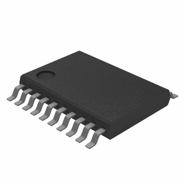
PACKAGING INFORMATION
20-LEAD PLASTIC, TSSOP PACKAGE TYPE V
.025 (.65) BSC
.169 (4.3)
.252 (6.4) BSC
.177 (4.5)
.252 (6.4)
.260 (6.6)
.047 (1.20)
.0075 (.19)
.0118 (.30)
.002 (.05)
.006 (.15)
(4.16)
.010 (.25)
(7.72)
Gage Plane
0 - 8
Seating Plane
.019 (.50)
.029 (.75)
(1.78)
(0.42)
Detail A (20X)
(0.65)
ALL MEASUREMENTS ARE TYPICAL
.031 (.80)
.041 (1.05)
See Detail “A”
NOTE: ALL DIMENSIONS IN INCHES (IN PARENTHESES IN MILLIMETERS)
© Copyright Intersil Americas LLC 2005. All Rights Reserved.
All trademarks and registered trademarks are the property of their respective owners.
For additional products, see www.intersil.com/en/products.html
Intersil products are manufactured, assembled and tested utilizing ISO9001 quality systems as noted
in the quality certifications found at www.intersil.com/en/support/qualandreliability.html
Intersil products are sold by description only. Intersil may modify the circuit design and/or specifications of products at any time without notice, provided that such
modification does not, in Intersil's sole judgment, affect the form, fit or function of the product. Accordingly, the reader is cautioned to verify that datasheets are
current before placing orders. Information furnished by Intersil is believed to be accurate and reliable. However, no responsibility is assumed by Intersil or its
subsidiaries for its use; nor for any infringements of patents or other rights of third parties which may result from its use. No license is granted by implication or
otherwise under any patent or patent rights of Intersil or its subsidiaries.
For information regarding Intersil Corporation and its products, see www.intersil.com
FN8147 Rev 0.00
March 17, 2005
Page 18 of 18
�