DATASHEET
X9268
Dual Supply/Low Power/256-Tap/2-Wire Bus Dual Digitally-Controlled (XDCP™)
Potentiometers
FN8172
Rev.4.00
August 29, 2006
FEATURES
DESCRIPTION
• Dual–Two Separate Potentiometers
• 256 Resistor Taps/Pot–0.4% Resolution
• 2-Wire Serial Interface for Write, Read, and
Transfer Operations of the Potentiometer
• Wiper Resistance, 100 typical @ V+ = 5V,
V- = -5V
• 16 Nonvolatile Data Registers for Each
Potentiometer
• Nonvolatile Storage of Multiple Wiper Positions
• Power-on Recall. Loads Saved Wiper Position on
Power-up.
• Standby Current VH, VL, and VW.
(5) n = 0, 1, 2, …,255; m =0, 1, 2, …, 254.
FN8172 Rev.4.00
August 29, 2006
Page 15 of 22
�X9268
D.C. OPERATING CHARACTERISTICS (Over the recommended operating conditions unless otherwise specified.)
Symbol
ICC1
Parameter
VCC supply current
(active)
Test Conditions
fSCL = 400kHz; VCC = +6V;
SDA = Open; (for 2-Wire, Active, Read and
Volatile Write States only)
fSCL = 400kHz; VCC = +6V;
SDA = Open; (for 2-Wire, Active,
Nonvolatile Write State only)
ICC2
VCC supply current
(nonvolatile write)
ISB
VCC current (standby)
ILI
Min.
Typ.
Max.
3
Units
mA
5
mA
VCC = +6V; VIN = VSS or VCC;
SDA = VCC; (for 2-Wire, Standby State only)
5
A
Input leakage current
VIN = VSS to VCC
10
A
ILO
Output leakage current
VOUT = VSS to VCC
10
A
VIH
Input HIGH voltage
VCC x 0.7
VCC + 1
V
VIL
Input LOW voltage
-1
VCC x 0.3
V
VOL
Output LOW voltage
0.4
V
VOH
Output HIGH voltage
IOL = 3mA
ENDURANCE AND DATA RETENTION
Parameter
Min.
Units
Minimum endurance
100,000
Data changes per bit per register
Data retention
100
years
CAPACITANCE
Symbol
CIN/OUT(6)
CIN(6)
Max.
Units
Test Conditions
Input / Output capacitance (SDA)
Test
8
pF
VOUT = 0V
Input capacitance (SCL, WP, A3, A2, A1 and A0)
6
pF
VIN = 0V
POWER-UP TIMING
Symbol
Parameter
tr VCC(6)
VCC Power-up rate
tPUR(7)
Power-up to initiation of read operation
Min.
Max.
Units
0.2
50
V/ms
1
ms
POWER-UP AND DOWN REQUIREMENTS
The are no restrictions on the sequencing of the bias supplies VCC, V+, and V- provided that all three supplies reach
their final values within 1msec of each other. At all times, the voltages on the potentiometer pins must be less than V+
and more than V-. The recall of the wiper position from nonvolatile memory is not in effect until all supplies reach their
final value. The VCC ramp rate spec is always in effect.
A.C. TEST CONDITIONS
Input Pulse Levels
Input rise and fall times
Input and output timing level
VCC x 0.1 to VCC x 0.9
10ns
VCC x 0.5
Notes: (6) This parameter is not 100% tested
(7) tPUR and tPUW are the delays required from the time the (last) power supply (VCC-) is stable until the specific instruction can be issued.
These parameters are periodically sampled and not 100% tested.
FN8172 Rev.4.00
August 29, 2006
Page 16 of 22
�X9268
EQUIVALENT A.C. LOAD CIRCUIT
5V
3V
1533
SDA pin
SPICE Macromodel
867
RTOTAL
RH
SDA pin
RL
CW
CL
100pF
100pF
CL
10pF
25pF
10pF
RW
AC TIMING
Symbol
Parameter
Min.
Max.
Units
400
kHz
fSCL
Clock Frequency
tCYC
Clock Cycle Time
2500
ns
tHIGH
Clock High Time
600
ns
tLOW
Clock Low Time
1300
ns
tSU:STA
Start Setup Time
600
ns
tHD:STA
Start Hold Time
600
ns
tSU:STO
Stop Setup Time
600
ns
tSU:DAT
SDA Data Input Setup Time
100
ns
tHD:DAT
SDA Data Input Hold Time
30
tR
SCL and SDA Rise Time
300
ns
tF
SCL and SDA Fall Time
300
ns
tAA
SCL Low to SDA Data Output Valid Time
0.9
s
tDH
SDA Data Output Hold Time
0
ns
TI
Noise Suppression Time Constant at SCL and SDA inputs
50
ns
tBUF
Bus Free Time (Prior to Any Transmission)
1200
ns
tSU:WPA
A0, A1 Setup Time
0
ns
tHD:WPA
A0, A1 Hold Time
0
ns
ns
HIGH-VOLTAGE WRITE CYCLE TIMING
Symbol
Parameter
tWR
High-voltage write cycle time (store instructions)
Typ.
Max.
Units
5
10
ms
XDCP TIMING
Symbol
Parameter
Min.
Max. Units
tWRPO
Wiper response time after the third (last) power supply is stable
5
10
s
tWRL
Wiper response time after instruction issued (all load instructions)
5
10
s
FN8172 Rev.4.00
August 29, 2006
Page 17 of 22
�X9268
TIMING DIAGRAMS
Start and Stop Timing
(START)
(STOP)
tR
tF
SCL
tSU:STA
tHD:STA
tSU:STO
tR
tF
SDA
Input Timing
tCYC
tHIGH
SCL
tLOW
SDA
tSU:DAT
tHD:DAT
tBUF
Output Timing
SCL
SDA
tAA
FN8172 Rev.4.00
August 29, 2006
tDH
Page 18 of 22
�X9268
XDCP Timing (for All Load Instructions)
(STOP)
SCL
LSB
SDA
tWRL
VWx
Write Protect and Device Address Pins Timing
(START)
SCL
(STOP)
...
(Any Instruction)
...
SDA
...
tSU:WPA
tHD:WPA
WP
A0, A1
FN8172 Rev.4.00
August 29, 2006
Page 19 of 22
�X9268
APPLICATIONS INFORMATION
Basic Configurations of Electronic Potentiometers
+VR
VR
RW
I
Three terminal Potentiometer;
Variable voltage divider
Two terminal Variable Resistor;
Variable current
Application Circuits
Noninverting Amplifier
VS
Voltage Regulator
+
VO
–
VIN
VO (REG)
317
R1
R2
Iadj
R1
R2
VO = (1+R2/R1)VS
VO (REG) = 1.25V (1+R2/R1)+Iadj R2
Offset Voltage Adjustment
R1
Comparator with Hysterisis
R2
VS
VS
–
+
100k
–
VO
+
+12V
FN8172 Rev.4.00
August 29, 2006
10k
}
10k
}
TL072
10k
VO
R1
R2
VUL = {R1/(R1+R2)} VO(max)
VLL = {R1/(R1+R2)} VO(min)
-12V
Page 20 of 22
�X9268
Application Circuits (continued)
Attenuator
Filter
C
VS
R2
R1
VO
–
–
VS
+
R
VO
+
R3
R4
R2
R1 = R2 = R3 = R4 = 10k
R1
GO = 1 + R2/R1
fc = 1/(2RC)
V O = G VS
-1/2 G +1/2
R2
}
VS
R1
}
Inverting Amplifier
Equivalent L-R Circuit
R2
C1
–
VS
VO
+
+
–
R1
ZIN
V O = G VS
G = - R2/R1
R3
ZIN = R2 + s R2 (R1 + R3) C1 = R2 + s Leq
(R1 + R3) >> R2
Function Generator
C
R2
–
+
R1
–
} RA
+
} RB
frequency R1, R2, C
amplitude RA, RB
FN8172 Rev.4.00
August 29, 2006
Page 21 of 22
�X9268
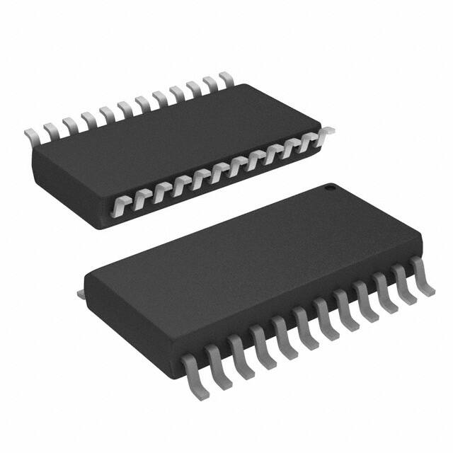
X9268
Small Outline Plastic Packages (SOIC)
M24.3 (JEDEC MS-013-AD ISSUE C)
N
24 LEAD WIDE BODY SMALL OUTLINE PLASTIC PACKAGE
INDEX
AREA
H
0.25(0.010) M
B M
INCHES
E
SYMBOL
-B1
2
3
L
SEATING PLANE
-A-
A
D
h x 45°
-C-
e
A1
B
0.25(0.010) M
C
0.10(0.004)
C A M
MIN
MAX
MIN
MAX
NOTES
A
0.0926
0.1043
2.35
2.65
-
A1
0.0040
0.0118
0.10
0.30
-
B
0.013
0.020
0.33
0.51
9
C
0.0091
0.0125
0.23
0.32
-
D
0.5985
0.6141
15.20
15.60
3
E
0.2914
0.2992
7.40
7.60
4
e
B S
0.05 BSC
1.27 BSC
-
H
0.394
0.419
10.00
10.65
-
h
0.010
0.029
0.25
0.75
5
L
0.016
0.050
0.40
1.27
6
N
NOTES:
MILLIMETERS
24
0°
24
8°
0°
1. Symbols are defined in the “MO Series Symbol List” in Section 2.2 of
Publication Number 95.
7
8°
Rev. 1 4/06
2. Dimensioning and tolerancing per ANSI Y14.5M-1982.
3. Dimension “D” does not include mold flash, protrusions or gate burrs.
Mold flash, protrusion and gate burrs shall not exceed 0.15mm
(0.006 inch) per side.
4. Dimension “E” does not include interlead flash or protrusions. Interlead flash and protrusions shall not exceed 0.25mm (0.010 inch) per
side.
5. The chamfer on the body is optional. If it is not present, a visual index
feature must be located within the crosshatched area.
6. “L” is the length of terminal for soldering to a substrate.
7. “N” is the number of terminal positions.
8. Terminal numbers are shown for reference only.
9. The lead width “B”, as measured 0.36mm (0.014 inch) or greater
above the seating plane, shall not exceed a maximum value of
0.61mm (0.024 inch)
10. Controlling dimension: MILLIMETER. Converted inch dimensions
are not necessarily exact.
© Copyright Intersil Americas LLC 2005-2006. All Rights Reserved.
All trademarks and registered trademarks are the property of their respective owners.
For additional products, see www.intersil.com/en/products.html
Intersil products are manufactured, assembled and tested utilizing ISO9001 quality systems as noted
in the quality certifications found at www.intersil.com/en/support/qualandreliability.html
Intersil products are sold by description only. Intersil may modify the circuit design and/or specifications of products at any time without notice, provided that such
modification does not, in Intersil's sole judgment, affect the form, fit or function of the product. Accordingly, the reader is cautioned to verify that datasheets are
current before placing orders. Information furnished by Intersil is believed to be accurate and reliable. However, no responsibility is assumed by Intersil or its
subsidiaries for its use; nor for any infringements of patents or other rights of third parties which may result from its use. No license is granted by implication or
otherwise under any patent or patent rights of Intersil or its subsidiaries.
For information regarding Intersil Corporation and its products, see www.intersil.com
FN8172 Rev.4.00
August 29, 2006
Page 22 of 22
�