PEDR48V256A-06
Issue Date: Oct. 17, 2011
MR48V256A
32,768-Word 8-Bit FeRAM (Ferroelectric Random Access Memory)
GENERAL DESCRIPTION
The MR48V256A is a nonvolatile 32,768-word x 8-bit ferroelectric random access memory (FeRAM) developed
in the ferroelectric process and silicon-gate CMOS technology. Unlike SRAMs, this device, whose cells are
nonvolatile, eliminates battery backup required to hold data. This device has no mechanisms of erasing and
programming memory cells and blocks, such as those used for various EEPROMs. Therefore, the write cycle
time can be equal to the read cycle time and the power consumption during a write can be reduced significantly.
The MR48V256A can be used in various applications, because the device is guaranteed for the write/read
tolerance of 1012 cycles per bit and the rewrite count can be extended significantly.
FEATURES
•
•
•
•
•
•
•
•
•
32,768-word 8-bit configuration
A single 3.3 V 0.3 V power supply
Read access time:
70 ns (Max.)
Write enable time:
70 ns (Min.)
Random read/write cycle time
150 ns (Min.)
Read/write tolerance
1012 cycles/bit
Data retention
10 years
Guaranteed operating temperature range
40 to 85C (Extended temperature version)
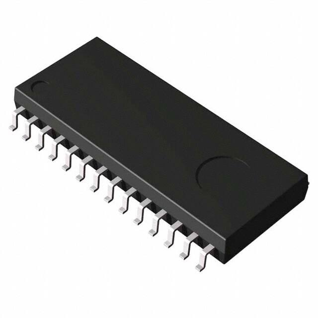
Package options:
28-pin plastic TSOPI (TSOP(1)28-08134-0.55-ZK)
PRODUCT FAMILY
Access Time
Family
MR48V256A
Relative to OE
Read/Write
Cycle Time
Package
Relative to CE
70ns
40ns
150ns
28pin TSOPI
1/12
�PEDR48V256A-06
MR48V256A
PIN CONFIGURATION
28-pin plastic TSOPI
OE#
A11
A9
A8
A13
WE#
VCC
A14
A12
A7
A6
A5
A4
A3
1
2
3
4
5
6
7
8
9
10
11
12
13
14
MR48V256A-XX
28
27
26
25
24
23
22
21
20
19
18
17
16
15
A10
CE#
DQ7
DQ6
DQ5
DQ4
DQ3
VSS
DQ2
DQ1
DQ0
A0
A1
A2
Note:
Signal names that end with # indicate that the pins are negative-true logic.
2/12
�PEDR48V256A-06
MR48V256A
PIN DESCRIPTIONS
Pin Name
CE#
OE#
WE#
A14 to A0
DQ7 to DQ0
VCC, VSS
Description
Chip enable (input, negative logic)
Latches an address by low input, activates the FeRAM, and enables a read or write
operation.
Output enable (input, negative logic)
The FeRAM is in read mode when the FeRAM is active and this pin is low, and data is
output after the specified time.
Write enable (input, negative logic)
The FeRAM is in write mode when the FeRAM is active and this pin is low, and data is
capture at the timing of WE#="H" or CE#="H", whichever is earlier.
Address (input)
The FeRAM captures an address at the timing when CE#="L" is established.
3-state data bus (input/output)
Outputs data in the read mode, and captures data in the write mode.
Power supply
Apply the specified voltage to VCC. Connect VSS to ground.
TRUTH TABLE
Operating Mode
CE#
WE#
Standby Mode
H
X
Address Latched
↓
X
Read Mode
L
H
Write Mode
L
↓
3/12
�PEDR48V256A-06
MR48V256A
ELECTRICAL CHARACTERISTICS
Absolute Maximum Ratings
Parameter
Rating
Symbol
Min.
Unit
Max.
Note
Pin Voltage (Input Signal)
VIN
–0.5
VCC + 0.5
V
Pin Voltage (Input/Output
Voltage)
VINQ, VOUTQ
–0.5
VCC + 0.5
V
VCC
–0.5
4.6
V
Tstg
–55
125
°C
Topr
–40
85
°C
Power Supply Voltage
Storage Temperature
(Extended Temperature
Version)
Operating Temperature
(Extended Temperature
Version)
Power Dissipation
PD
1,000
mW
Allowable Input Current
IIN
±20
mA
Ta=25°C
IOUT
±20
mA
Ta=25°C
Allowable Output Current
Note:
The application of stress (voltage, current, or temperature) that exceeds the absolute maximum rating may
damage the device. Therefore, do not allow actual characteristics to exceed any one parameter ratings
Recommended Operating Conditions
Parameter
Power Supply Voltage
Ground Voltage
Symbol
VCC
VSS
Min.
3.0
0.0
Max.
3.3
0.0
Unit
V
V
Note
Input High Voltage
VIH
VCC x 0.8
VCC + 0.3
V
1
Input Low Voltage
VIL
–0.3
VCC x 0.15
V
2
Operating Temperature (Extended
Temperature Version)
Ta
–40
85
°C
Notes:
1. Overshoots with the pulse width of 20 ns or less and the voltage of VCC + 1.0 V or less are allowed.
2. Undershoots with the pulse width of 20 ns or less and the voltage of 1.0 V or more are allowed.
Capacitance
Parameter
Input Capacitance
Input/Output Capacitance
Symbol
CIN
COUT
Min.
Max.
6
8
Unit
pF
pF
Note
1
1
Note:
Sampling value. Measurement conditions are VIN = VOUT = GND, f = 1MHz, and Ta = 25°C
4/12
�PEDR48V256A-06
MR48V256A
DC Characteristics
(Under recommended operating conditions)
Parameter
Symbol
Output High Voltage
VOH
Output Low Voltage
VOL
Condition
Min.
Max.
Unit
IOH = –2 mA
VCC 0.85
V
Note
IOL = 2 mA
VCC 0.15
V
Input Leakage Current
ILI
–10
10
µA
Output Leakage Current
ILO
–10
10
µA
Power Supply Current
(Standby)
ICCS
VIN = 0.2V or VCC–0.2V,
CE# = VCC–0.2V
IOUT = 0 mA
400
µA
Power Supply Current
(Operating)
ICCA
10
mA
Read Cycle, tRC = Min.
VIN = 0.2V or VCC–0.2V,
CE# = 0.2V, IOUT = 0 mA
1
Note:
1. Average current. Address change must be one time or less during time tRC.
Read/Write Cycles and Data Retention
(Under recommended operating conditions)
Parameter
Read/Write Cycle
Data Retention
Min.
1012
10
Max.
Unit
Cycle
Year
Note
1
Notes:
1. This is applicable to the read cycle, write cycle, and CE-only cycle counts.
This is the cycle count per bit (for one address).
5/12
�PEDR48V256A-06
MR48V256A
AC Characteristics (Read Cycle)
(Under recommended operating conditions)
Parameter
-70
Symbol
Unit
Min.
Max.
Address Set-up Time
tAVEL
5
―
ns
Address Hold Time (CE#)
tELAX
10
―
ns
CE# High Pulse Width
tEHEL
80
―
ns
Output Hold Time (CE#)
tEHQX
5
―
ns
Output High Impedance Time (CE#)
tEHQZ
―
25
ns
CE# Active Time
tELEH
70
2000
ns
Read Cycle Time (CE# cycle Time)
tELEL
150
―
ns
CE# Access Time
tELQV
―
70
ns
Output Low Impedance Time (CE#)
tEHQX
5
―
ns
Output Hold Time (OE#)
tGHQX
5
―
ns
Output High Impedance Time (OE#)
tGHQZ
―
25
ns
OE# Access Time
tGLQV
―
40
ns
Output Low Impedance Time (OE#)
tGLQX
5
―
ns
Note
1
1
Notes:
The read data is output at the point where all of the maximum values of tELQV and tGLQV are satisfied.
6/12
�PEDR48V256A-06
MR48V256A
AC Characteristics (Write Cycle)
(Under recommended operating conditions) Note 1
Parameter
-70
Symbol
Unit
Min.
Max.
Note
Address Set-up Time
tAVEL
5
―
ns
Data Set-up Time (WE#)
tDVWH
20
―
ns
Data Set-up Time (CE#)
tDVEH
40
―
ns
Address Hold Time (CE#)
tELAX
10
―
ns
Data Hold Time (CE#)
tEHDX
0
―
ns
CE# High Pulse Width
tEHEL
80
―
ns
CE# Active Time
tELEH
70
2000
ns
Write Cycle Time (CE# Cycle Time)
tELEL
150
―
ns
Write Command Set-up Time (CE# to WE#)
tELWH
70
―
ns
Data Hold Time (WE#)
tWHDX
0
―
ns
Write Command Pulse Width
tWLWH
40
―
ns
WE# Set-up Time (CE#)
tELWL
0
―
ns
1
WE# Hold Time (CE#)
tWHEH
0
―
ns
1
Notes:
“CE# controled WRITE”mode or “OE# controled WRITE” mode is decided by the rerationship between CE#
and OE#.
7/12
�PEDR48V256A-06
MR48V256A
Timing Diagrams
Read cycle
tELEL
tELEH
tEHEL
CE#
tELAX
An
Address Valid
tAVEL
tGLQV
tGHQX
OE#
tGLQX
tGHQZ
tELQX
DQ
Valid Data Out
tEHQX
tELQV
tEHQZ
Note: WE# = “H”
Write cycle
tELEL
tELEH
tEHEL
CE#
tELAX
An
Address Valid
tAVEL
WE#
tELWL
tWHEH
OE#
tDVEH
DQ
tEHDX
Data In
8/12
�PEDR48V256A-06
MR48V256A
WE Control Write Cycle
tELEH
tEHEL
CE#
tELWH
tELAX
An
Address Valid
tAVEL
WE#
tWHEH
tELWL
tWLWH
OE#
tDVWH
DQ
tWHDX
Data In
9/12
�PEDR48V256A-06
MR48V256A
CE-Only Cycle
An
Invalid Address In
Address Valid
tAVEL
tELAX
tELEH
tEHEL
CE#
Note: OE# = “H”, WE# = “H”, DQ = High-Z
Power-On and Power-Off Characteristics
(Under recommended operating conditions)
Parameter
Power-On CE# High Hold Time
Power-Off CE# High Hold Time
Power-On Interval Time
Symbol
tVHEL
tEHVL
tVLVH
Min.
50
100
1
Max.
Unit
s
ns
s
Note
1, 2
1
2
Notes:
1. To prevent an erroneous operation, be sure to maintain CE#="H", and set the FeRAM in an inactive state
(standby mode) before and after power-on and power-off.
2. Powering on at the intermediate voltage level will cause an erroneous operation; thus, be sure to power up
from 0 V.
3. Enter all signals at the same time as power-on or enter all signals after power-on.
Power-On and Power-Off Sequences
tEHVL
tVHEL
VCC
VCC
VCC Min.
VCC Min.
VIH Min.
VIH Min.
tVLVH
VIL Max.
CE#
0V
VIL Max.
CE#
0V
10/12
�PEDR48V256A-06
MR48V256A
REVISION HISTORY
Page
Document No.
Date
Previous
Edition
Current
Edition
PEDR48V256A-01
Mar. 30, 2010
–
–
Preliminary edition 1 from PJDR48V256A-05
1
1
Package code name
PEDR48V256A-02
Aug. 26, 2010
1,4,5
1,4,5
PEDR48V256A-03
Dec. 02, 2010
4
4
PEDR48V256A-04
Mar. 04, 2011
1,2,4
1,2,4
PEDR48V256A-05
Sep. 05, 2011
8,9
10
8,9
10
PEDR48V256A-06
Oct. 17, 2011
1-12
1-12
Description
Input Voltage
2.0/0.8 ⇒ Vcc x 0.8 / Vcc x 0.2
Input Voltage VIL Vcc x 0.2 ⇒ Vcc x 0.15
Pin name VDD ⇒ VCC
temperature version ⇒ Extended version
OE# wave in Timing chart
Input signal state in power-on
Changed corporate name and logo to LAPIS
Semiconductor.
11/12
�PEDR48V256A-06
MR48V256A
NOTES
No copying or reproduction of this document, in part or in whole, is permitted without the consent of LAPIS
Semiconductor Co., Ltd.
The content specified herein is subject to change for improvement without notice.
The content specified herein is for the purpose of introducing LAPIS Semiconductor's products (hereinafter
"Products"). If you wish to use any such Product, please be sure to refer to the specifications, which can be
obtained from LAPIS Semiconductor upon request.
Examples of application circuits, circuit constants and any other information contained herein illustrate the
standard usage and operations of the Products. The peripheral conditions must be taken into account when
designing circuits for mass production.
Great care was taken in ensuring the accuracy of the information specified in this document. However, should
you incur any damage arising from any inaccuracy or misprint of such information, LAPIS Semiconductor shall
bear no responsibility for such damage.
The technical information specified herein is intended only to show the typical functions of and examples of
application circuits for the Products. LAPIS Semiconductor does not grant you, explicitly or implicitly, any
license to use or exercise intellectual property or other rights held by LAPIS Semiconductor and other parties.
LAPIS Semiconductor shall bear no responsibility whatsoever for any dispute arising from the use of such
technical information.
The Products specified in this document are intended to be used with general-use electronic equipment or
devices (such as audio visual equipment, office-automation equipment, communication devices, electronic
appliances and amusement devices).
The Products specified in this document are not designed to be radiation tolerant.
While LAPIS Semiconductor always makes efforts to enhance the quality and reliability of its Products, a
Product may fail or malfunction for a variety of reasons.
Please be sure to implement in your equipment using the Products safety measures to guard against the
possibility of physical injury, fire or any other damage caused in the event of the failure of any Product, such as
derating, redundancy, fire control and fail-safe designs. LAPIS Semiconductor shall bear no responsibility
whatsoever for your use of any Product outside of the prescribed scope or not in accordance with the instruction
manual.
The Products are not designed or manufactured to be used with any equipment, device or system which requires
an extremely high level of reliability the failure or malfunction of which may result in a direct threat to human
life or create a risk of human injury (such as a medical instrument, transportation equipment, aerospace
machinery, nuclear-reactor controller, fuel-controller or other safety device). LAPIS Semiconductor shall bear
no responsibility in any way for use of any of the Products for the above special purposes. If a Product is
intended to be used for any such special purpose, please contact a ROHM sales representative before purchasing.
If you intend to export or ship overseas any Product or technology specified herein that may be controlled under
the Foreign Exchange and the Foreign Trade Law, you will be required to obtain a license or permit under the
Law.
Copyright 2011 LAPIS Semiconductor Co., Ltd.
12/12
�


 工商网监
湘ICP备2023018690号
工商网监
湘ICP备2023018690号
