C8051F96x
Ultra Low Power 128K, LCD MCU Family
Ultra Low Power Consumption at 3.6 V
- 130 µA/MHz Low-Power Active mode with dc-dc
enabled
- 120 nA sleep current w/ data retention; POR monitor
enabled
- 450 nA sleep mode with SmaRTClock
(internal LFO)
- 600 nA sleep mode with SmaRTClock (ext. crystal)
- 2 µs wakeup time; 1.5 µA analog settling time
12-Bit; 16 Ch. Analog-to-Digital Converter
- Up to 75 ksps (12-bit mode) or 300 ksps
(10-bit mode)
- External pin or internal VREF (no ext cap required)
- On-chip voltage reference; 0.5x gain allows measuring voltages up to twice the reference voltage
- Autonomous burst mode with 16-bit auto-averaging
accumulator
- Integrated temperature sensor
Two Low Current Comparators
- Programmable hysteresis and response time
- Configurable as wake-up or reset source
Internal 6-Bit Current Reference
- Up to ±500 µA; source and sink capability
- Enhanced resolution via PWM interpolation
Integrated LCD Controller
- Supports up to 128 segments (32x4)
- LCD controller consumes only 400 nA for
32-segment static display
- Integrated charge pump for contrast control
Metering-Specific Peripherals
- DC-DC buck converter allows dynamic voltage
scaling for maximum efficiency (250 mW output)
- Sleep-mode pulse accumulator with programmable
switch, de-bounce and pull-up control; interfaces
directly to metering sensor
- Data Packet Processing Engine (DPPE) includes
hardware AES, DMA, CRC and encoding blocks for
acceleration of wireless protocols
Wake
Reset
C2CK/RST
Debug /
Programming
Hardware
UART
256 Byte SRAM
Timers
0, 1, 2, 3
8092 Byte XRAM
PCA/WDT
DMA
Analog
Power
VDD
VDC
VREG
Digital
Power
IND
DC/DC Buck
Converter
LCD Charge
Pump
XTAL1
XTAL2
GND
XTAL3
XTAL4
Low Power
20 MHz
Oscillator
External
Oscillator
Circuit
Enhanced
smaRTClock
Oscillator
LCD (up to 4x32)
SFR
Bus
EMIF
Pulse Counter
Analog Peripherals
Internal
External
VREF
VREF
A
M
U
X
12-bit
75ksps
ADC
Rev. 1.0 7/13
VDD
VREF
Temp
Sensor
P3-6
Drivers
32
P7
Driver
16
P3.0...P6.7
P7.0/C2D
GND
CP0, CP0A
System Clock
Configuration
Port 2
Drivers
Crossbar Control
Precision
24.5 MHz
Oscillator
GNDDC
CAP
SPI 1
(DMA Enabled)
AES
Engine
SYSCLK
P2.0/SCK1
P2.1/MISO1
P2.2/MOSI1
P2.3/NSS1
P2.4
P2.5
P2.6
P2.7
SPI 0
CRC
Engine
Encoder
VBATDC
Port 1
Drivers
P1.0/PC0
P1.1/PC1
P1.2/XTAL3
P1.3/XTAL4
P1.4
P1.5/INT5
P1.6/INT6
P1.7
Priority
Crossbar
Decoder
SMBus
VBAT
Port 0
Drivers
P0.0/VREF
P0.1/AGND
P0.2/XTAL1
P0.3/XTAL2
P0.4/TX
P0.5/RX
P0.6/CNVSTR
P0.7
Digital Peripherals
128k Byte ISP Flash
Program Memory
C2D
VBAT
Temperature Range: –40 to +85 °C
Port I/O Configuration
CIP-51 8051
Controller Core
Power On
Reset/PMU
High-Speed 8051 µC Core
- Pipelined instruction architecture; executes 70% of
instructions in 1 or 2 system clocks
Memory
- Up to 128 kB Flash; In-system programmable; Full
read/write/erase functionality over supply range
- Up to 8 kB internal data RAM
Digital Peripherals
- 57 or 34 port I/O; All 5 V tolerant with high sink
current and programmable drive strength
- Hardware SMBus™ (I2C™ Compatible), 2 x SPI™,
and UART serial ports available concurrently
- Four general purpose 16-bit counter/timers
- Programmable 16-bit counter/timer array with six
capture/compare modules and watchdog timer
Clock Sources
- Precision Internal oscillator: 24.5 MHz, 2% accuracy
supports UART operation; spread-spectrum mode
for reduced EMI
- Low power internal oscillator: 20 MHz
- External oscillator: Crystal, RC, C, or CMOS Clock
- SmaRTClock oscillator: 32 kHz Crystal or 16.4 kHz
internal LFO
On-Chip Debug
- On-chip debug circuitry facilitates full-speed, nonintrusive in-system debug (no emulator required)
- Provides 4 breakpoints, single stepping
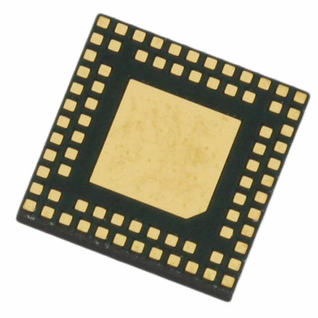
Packages
- 76-pin DQFN (6 x 6 mm)
- 40-pin QFN (6 x 6 mm)
- 80-pin TQFP (12 x 12 mm)
CP1, CP1A
+
-
+
-
Comparators
Copyright © 2013 by Silicon Laboratories
C8051F96x
�C8051F96x
2
Rev. 1.0
�C8051F96x
Table of Contents
1. System Overview ..................................................................................................... 22
1.1. CIP-51™ Microcontroller Core .......................................................................... 28
1.1.1. Fully 8051 Compatible .............................................................................. 28
1.1.2. Improved Throughput................................................................................ 28
1.1.3. Additional Features ................................................................................... 28
1.2. Port Input/Output ............................................................................................... 29
1.3. Serial Ports ........................................................................................................ 30
1.4. Programmable Counter Array............................................................................ 30
1.5. SAR ADC with 16-bit Auto-Averaging Accumulator and Autonomous
Low Power Burst Mode ..................................................................................... 31
1.6. Programmable Current Reference (IREF0)....................................................... 32
1.7. Comparators...................................................................................................... 32
2. Ordering Information ............................................................................................... 34
3. Pinout and Package Definitions ............................................................................. 35
3.1. DQFN-76 Package Specifications ..................................................................... 46
3.1.1. Package Drawing ...................................................................................... 46
3.1.2. Land Pattern.............................................................................................. 47
3.1.3. Soldering Guidelines ................................................................................. 48
3.2. QFN-40 Package Specifications........................................................................ 50
3.3. TQFP-80 Package Specifications...................................................................... 52
3.3.1. Soldering Guidelines ................................................................................. 55
4. Electrical Characteristics ........................................................................................ 56
4.1. Absolute Maximum Specifications..................................................................... 56
4.2. Electrical Characteristics ................................................................................... 57
5. SAR ADC with 16-bit Auto-Averaging Accumulator and Autonomous
Low Power Burst Mode........................................................................................... 78
5.1. Output Code Formatting .................................................................................... 78
5.2. Modes of Operation ........................................................................................... 80
5.2.1. Starting a Conversion................................................................................ 80
5.2.2. Tracking Modes......................................................................................... 80
5.2.3. Burst Mode................................................................................................ 82
5.2.4. Settling Time Requirements...................................................................... 83
5.2.5. Gain Setting .............................................................................................. 83
5.3. 8-Bit Mode ......................................................................................................... 84
5.4. 12-Bit Mode ....................................................................................................... 84
5.5. Low Power Mode............................................................................................... 85
5.6. Programmable Window Detector....................................................................... 91
5.6.1. Window Detector In Single-Ended Mode .................................................. 93
5.6.2. ADC0 Specifications ................................................................................. 94
5.7. ADC0 Analog Multiplexer .................................................................................. 95
5.8. Temperature Sensor.......................................................................................... 97
5.8.1. Calibration ................................................................................................. 97
5.9. Voltage and Ground Reference Options ......................................................... 100
Rev. 1.0
2
�C8051F96x
5.10. External Voltage Reference........................................................................... 101
5.11. Internal Voltage Reference............................................................................ 101
5.12. Analog Ground Reference............................................................................. 101
5.13. Temperature Sensor Enable ......................................................................... 101
5.14. Voltage Reference Electrical Specifications .................................................. 102
6. Programmable Current Reference (IREF0).......................................................... 103
6.1. PWM Enhanced Mode..................................................................................... 103
6.2. IREF0 Specifications ....................................................................................... 104
7. Comparators........................................................................................................... 105
7.1. Comparator Inputs........................................................................................... 105
7.2. Comparator Outputs ........................................................................................ 106
7.3. Comparator Response Time ........................................................................... 107
7.4. Comparator Hysterisis ..................................................................................... 107
7.5. Comparator Register Descriptions .................................................................. 108
7.6. Comparator0 and Comparator1 Analog Multiplexers ...................................... 112
8. CIP-51 Microcontroller........................................................................................... 115
8.1. Instruction Set.................................................................................................. 116
8.1.1. Instruction and CPU Timing .................................................................... 116
8.2. CIP-51 Register Descriptions .......................................................................... 121
9. Memory Organization ............................................................................................ 124
9.1. Program Memory............................................................................................. 124
9.1.1. MOVX Instruction and Program Memory ................................................ 127
9.2. Data Memory ................................................................................................... 127
9.2.1. Internal RAM ........................................................................................... 127
9.2.2. External RAM .......................................................................................... 128
10. External Data Memory Interface and On-Chip XRAM ....................................... 129
10.1. Accessing XRAM........................................................................................... 129
10.1.1. 16-Bit MOVX Example .......................................................................... 129
10.1.2. 8-Bit MOVX Example ............................................................................ 129
10.2. Configuring the External Memory Interface ................................................... 130
10.3. Port Configuration.......................................................................................... 130
10.4. Multiplexed and Non-multiplexed Selection................................................... 134
10.4.1. Multiplexed Configuration...................................................................... 134
10.4.2. Non-multiplexed Configuration.............................................................. 134
10.5. Memory Mode Selection................................................................................ 135
10.5.1. Internal XRAM Only .............................................................................. 136
10.5.2. Split Mode without Bank Select............................................................. 136
10.5.3. Split Mode with Bank Select.................................................................. 136
10.5.4. External Only......................................................................................... 136
10.6. Timing .......................................................................................................... 137
10.6.1. Non-Multiplexed Mode .......................................................................... 139
10.6.2. Multiplexed Mode .................................................................................. 142
11. Direct Memory Access (DMA0)........................................................................... 146
11.1. DMA0 Architecture ........................................................................................ 147
11.2. DMA0 Arbitration ........................................................................................... 148
3
Rev. 1.0
�C8051F96x
11.2.1. DMA0 Memory Access Arbitration ........................................................ 148
11.2.2. DMA0 Channel Arbitration .................................................................... 148
11.3. DMA0 Operation in Low Power Modes ......................................................... 148
11.4. Transfer Configuration................................................................................... 149
12. Cyclic Redundancy Check Unit (CRC0)............................................................. 160
12.1. 16-bit CRC Algorithm..................................................................................... 160
12.3. Preparing for a CRC Calculation ................................................................... 163
12.4. Performing a CRC Calculation ...................................................................... 163
12.5. Accessing the CRC0 Result .......................................................................... 163
12.6. CRC0 Bit Reverse Feature............................................................................ 167
13. DMA-Enabled Cyclic Redundancy Check Module (CRC1)............................... 168
13.1. Polynomial Specification................................................................................ 168
13.2. Endianness.................................................................................................... 169
13.3. CRC Seed Value ........................................................................................... 170
13.4. Inverting the Final Value................................................................................ 170
13.5. Flipping the Final Value ................................................................................. 170
13.6. Using CRC1 with SFR Access ...................................................................... 171
13.7. Using the CRC1 module with the DMA ......................................................... 171
14. Advanced Encryption Standard (AES) Peripheral ............................................ 175
14.1. Hardware Description .................................................................................... 176
14.1.1. AES Encryption/Decryption Core .......................................................... 177
14.1.2. Data SFRs............................................................................................. 177
14.1.3. Configuration sfrs .................................................................................. 178
14.1.4. Input Multiplexer.................................................................................... 178
14.1.5. Output Multiplexer ................................................................................. 178
14.1.6. Internal State Machine .......................................................................... 178
14.2. Key Inversion................................................................................................. 179
14.2.1. Key Inversion using DMA...................................................................... 180
14.2.2. Key Inversion using SFRs..................................................................... 181
14.2.3. Extended Key Output Byte Order.......................................................... 182
14.2.4. Using the DMA to unwrap the extended Key ........................................ 183
14.3. AES Block Cipher .......................................................................................... 184
14.4. AES Block Cipher Data Flow......................................................................... 185
14.4.1. AES Block Cipher Encryption using DMA ............................................. 186
14.4.2. AES Block Cipher Encryption using SFRs ............................................ 187
14.5. AES Block Cipher Decryption........................................................................ 188
14.5.1. AES Block Cipher Decryption using DMA............................................. 188
14.5.2. AES Block Cipher Decryption using SFRs............................................ 189
14.6. Block Cipher Modes ...................................................................................... 190
14.6.1. Cipher Block Chaining Mode................................................................. 190
14.6.2. CBC Encryption Initialization Vector Location....................................... 192
14.6.3. CBC Encryption using DMA .................................................................. 192
14.6.4. CBC Decryption .................................................................................... 195
14.6.5. Counter Mode ....................................................................................... 198
14.6.6. CTR Encryption using DMA .................................................................. 200
Rev. 1.0
4
�C8051F96x
15. Encoder/Decoder ................................................................................................. 207
15.1. Manchester Encoding.................................................................................... 208
15.2. Manchester Decoding.................................................................................... 209
15.3. Three-out-of-Six Encoding............................................................................ 210
15.4. Three-out-of-Six Decoding ............................................................................ 211
15.5. Encoding/Decoding with SFR Access ........................................................... 212
15.6. Decoder Error Interrupt.................................................................................. 212
15.7. Using the ENC0 module with the DMA.......................................................... 213
16. Special Function Registers................................................................................. 216
16.1. SFR Paging ................................................................................................... 216
16.2. Interrupts and SFR Paging ............................................................................ 216
17. Interrupt Handler.................................................................................................. 232
17.1. Enabling Interrupt Sources ............................................................................ 232
17.2. MCU Interrupt Sources and Vectors.............................................................. 232
17.3. Interrupt Priorities .......................................................................................... 233
17.4. Interrupt Latency............................................................................................ 233
17.5. Interrupt Register Descriptions ...................................................................... 235
17.6. External Interrupts INT0 and INT1................................................................. 242
18. Flash Memory....................................................................................................... 244
18.1. Programming the Flash Memory ................................................................... 244
18.1.1. Flash Lock and Key Functions .............................................................. 244
18.1.2. Flash Erase Procedure ......................................................................... 244
18.1.3. Flash Write Procedure .......................................................................... 245
18.1.4. Flash Write Optimization ....................................................................... 246
18.2. Non-volatile Data Storage ............................................................................. 247
18.3. Security Options ............................................................................................ 247
18.4. Determining the Device Part Number at Run Time ....................................... 249
18.5. Flash Write and Erase Guidelines ................................................................. 250
18.5.1. VDD Maintenance and the VDD Monitor .............................................. 250
18.5.2. PSWE Maintenance .............................................................................. 251
18.5.3. System Clock ........................................................................................ 251
18.6. Minimizing Flash Read Current ..................................................................... 252
19. Power Management ............................................................................................. 257
19.1. Normal Mode ................................................................................................. 258
19.2. Idle Mode....................................................................................................... 258
19.3. Stop Mode ..................................................................................................... 259
19.4. Low Power Idle Mode .................................................................................... 259
19.5. Suspend Mode .............................................................................................. 263
19.6. Sleep Mode ................................................................................................... 263
19.7. Configuring Wakeup Sources........................................................................ 264
19.8. Determining the Event that Caused the Last Wakeup................................... 264
19.9. Power Management Specifications ............................................................... 268
20. On-Chip DC-DC Buck Converter (DC0).............................................................. 269
20.1. Startup Behavior............................................................................................ 270
20.4. Optimizing Board Layout ............................................................................... 271
5
Rev. 1.0
�C8051F96x
20.5. Selecting the Optimum Switch Size............................................................... 271
20.6. DC-DC Converter Clocking Options .......................................................... 271
20.7. Bypass Mode................................................................................................. 272
20.8. DC-DC Converter Register Descriptions ....................................................... 272
20.9. DC-DC Converter Specifications ................................................................... 276
21. Voltage Regulator (VREG0)................................................................................. 277
21.1. Voltage Regulator Electrical Specifications ................................................... 277
22. Reset Sources ...................................................................................................... 278
22.1. Power-On Reset ............................................................................................ 279
22.2. Power-Fail Reset ........................................................................................... 280
22.3. External Reset ............................................................................................... 283
22.4. Missing Clock Detector Reset ....................................................................... 283
22.5. Comparator0 Reset ....................................................................................... 283
22.6. PCA Watchdog Timer Reset ......................................................................... 283
22.7. Flash Error Reset .......................................................................................... 284
22.8. SmaRTClock (Real Time Clock) Reset ......................................................... 284
22.9. Software Reset .............................................................................................. 284
23. Clocking Sources................................................................................................. 286
23.1. Programmable Precision Internal Oscillator .................................................. 287
23.2. Low Power Internal Oscillator........................................................................ 287
23.3. External Oscillator Drive Circuit..................................................................... 287
23.3.1. External Crystal Mode........................................................................... 287
23.3.2. External RC Mode................................................................................. 289
23.3.3. External Capacitor Mode....................................................................... 290
23.3.4. External CMOS Clock Mode ................................................................. 290
23.4. Special Function Registers for Selecting and Configuring the
System Clock ................................................................................................ 291
24. SmaRTClock (Real Time Clock).......................................................................... 295
24.1. SmaRTClock Interface .................................................................................. 296
24.1.1. SmaRTClock Lock and Key Functions.................................................. 297
24.1.2. Using RTC0ADR and RTC0DAT to Access SmaRTClock
Internal Registers.................................................................................. 297
24.1.3. SmaRTClock Interface Autoread Feature ............................................. 297
24.1.4. RTC0ADR Autoincrement Feature........................................................ 297
24.2. SmaRTClock Clocking Sources .................................................................... 300
24.2.1. Using the SmaRTClock Oscillator with a Crystal or
External CMOS Clock ........................................................................... 300
24.2.2. Using the SmaRTClock Oscillator in Self-Oscillate Mode..................... 301
24.2.3. Using the Low Frequency Oscillator (LFO) ........................................... 301
24.2.4. Programmable Load Capacitance......................................................... 301
24.2.5. Automatic Gain Control (Crystal Mode Only) and SmaRTClock
Bias Doubling ........................................................................................ 302
24.2.6. Missing SmaRTClock Detector ............................................................. 304
24.2.7. SmaRTClock Oscillator Crystal Valid Detector ..................................... 304
24.3. SmaRTClock Timer and Alarm Function ....................................................... 304
Rev. 1.0
6
�C8051F96x
24.3.1. Setting and Reading the SmaRTClock Timer Value ............................. 304
24.3.2. Setting a SmaRTClock Alarm ............................................................... 305
24.3.3. Software Considerations for using the SmaRTClock
Timer and Alarm ................................................................................... 305
25. Low-Power Pulse Counter .................................................................................. 312
25.1. Counting Modes ............................................................................................ 313
25.2. Reed Switch Types........................................................................................ 314
25.3. Programmable Pull-Up Resistors .................................................................. 315
25.4. Automatic Pull-Up Resistor Calibration ......................................................... 317
25.5. Sample Rate.................................................................................................. 317
25.6. Debounce ...................................................................................................... 317
25.7. Reset Behavior .............................................................................................. 318
25.8. Wake up and Interrupt Sources..................................................................... 318
25.9. Real-Time Register Access ........................................................................... 319
25.10. Advanced Features ..................................................................................... 319
25.10.1. Quadrature Error ................................................................................. 319
25.10.2. Flutter Detection.................................................................................. 320
26. LCD Segment Driver ............................................................................................ 334
26.1. Configuring the LCD Segment Driver ............................................................ 334
26.2. Mapping Data Registers to LCD Pins............................................................ 335
26.3. LCD Contrast Adjustment.............................................................................. 338
26.3.1. Contrast Control Mode 1 (Bypass Mode).............................................. 338
26.3.2. Contrast Control Mode 2 (Minimum Contrast Mode) ............................ 339
26.3.3. Contrast Control Mode 3 (Constant Contrast Mode)............................. 339
26.3.4. Contrast Control Mode 4 (Auto-Bypass Mode) ..................................... 340
26.4. Adjusting the VBAT Monitor Threshold ......................................................... 344
26.5. Setting the LCD Refresh Rate ....................................................................... 345
26.6. Blinking LCD Segments................................................................................. 346
26.7. Advanced LCD Optimizations........................................................................ 348
27. Port Input/Output ................................................................................................. 351
27.1. Port I/O Modes of Operation.......................................................................... 352
27.1.1. Port Pins Configured for Analog I/O...................................................... 352
27.1.2. Port Pins Configured For Digital I/O...................................................... 352
27.1.3. Interfacing Port I/O to High Voltage Logic............................................. 353
27.1.4. Increasing Port I/O Drive Strength ........................................................ 353
27.2. Assigning Port I/O Pins to Analog and Digital Functions............................... 353
27.2.1. Assigning Port I/O Pins to Analog Functions ........................................ 353
27.2.2. Assigning Port I/O Pins to Digital Functions.......................................... 354
27.2.3. Assigning Port I/O Pins to External Digital Event Capture Functions ... 354
27.3. Priority Crossbar Decoder ............................................................................. 355
27.4. Port Match ..................................................................................................... 361
27.5. Special Function Registers for Accessing and Configuring Port I/O ............. 363
28. SMBus................................................................................................................... 381
28.1. Supporting Documents .................................................................................. 382
28.2. SMBus Configuration..................................................................................... 382
7
Rev. 1.0
�C8051F96x
28.3. SMBus Operation .......................................................................................... 382
28.3.1. Transmitter Vs. Receiver....................................................................... 383
28.3.2. Arbitration.............................................................................................. 383
28.3.3. Clock Low Extension............................................................................. 383
28.3.4. SCL Low Timeout.................................................................................. 383
28.3.5. SCL High (SMBus Free) Timeout ......................................................... 384
28.4. Using the SMBus........................................................................................... 384
28.4.1. SMBus Configuration Register.............................................................. 384
28.4.2. SMB0CN Control Register .................................................................... 388
28.4.3. Hardware Slave Address Recognition .................................................. 390
28.4.4. Data Register ........................................................................................ 393
28.5. SMBus Transfer Modes................................................................................. 393
28.5.1. Write Sequence (Master) ...................................................................... 393
28.5.2. Read Sequence (Master) ...................................................................... 394
28.5.3. Write Sequence (Slave) ........................................................................ 395
28.5.4. Read Sequence (Slave) ........................................................................ 396
28.6. SMBus Status Decoding................................................................................ 397
29. UART0 ................................................................................................................... 402
29.1. Enhanced Baud Rate Generation.................................................................. 403
29.2. Operational Modes ........................................................................................ 404
29.2.1. 8-Bit UART ............................................................................................ 404
29.2.2. 9-Bit UART ............................................................................................ 404
29.3. Multiprocessor Communications ................................................................... 405
30. Enhanced Serial Peripheral Interface (SPI0) ..................................................... 411
30.1. Signal Descriptions........................................................................................ 412
30.1.1. Master Out, Slave In (MOSI)................................................................. 412
30.1.2. Master In, Slave Out (MISO)................................................................. 412
30.1.3. Serial Clock (SCK) ................................................................................ 412
30.1.4. Slave Select (NSS) ............................................................................... 412
30.2. SPI0 Master Mode Operation ........................................................................ 412
30.3. SPI0 Slave Mode Operation .......................................................................... 414
30.4. SPI0 Interrupt Sources .................................................................................. 415
30.5. Serial Clock Phase and Polarity .................................................................... 415
30.6. SPI Special Function Registers ..................................................................... 417
32. Timers ................................................................................................................... 444
32.1. Timer 0 and Timer 1 ...................................................................................... 446
32.1.1. Mode 0: 13-bit Counter/Timer ............................................................... 446
32.1.2. Mode 1: 16-bit Counter/Timer ............................................................... 447
32.1.3. Mode 2: 8-bit Counter/Timer with Auto-Reload..................................... 447
32.1.4. Mode 3: Two 8-bit Counter/Timers (Timer 0 Only)................................ 448
32.2. Timer 2 .......................................................................................................... 454
32.2.1. 16-bit Timer with Auto-Reload............................................................... 454
32.2.2. 8-bit Timers with Auto-Reload............................................................... 455
32.2.3. Comparator 0/SmaRTClock Capture Mode .......................................... 455
32.3. Timer 3 .......................................................................................................... 460
Rev. 1.0
8
�C8051F96x
32.3.1. 16-bit Timer with Auto-Reload............................................................... 460
32.3.2. 8-Bit Timers with Auto-Reload .............................................................. 461
32.3.3. SmaRTClock/External Oscillator Capture Mode ................................... 461
33. Programmable Counter Array............................................................................. 466
33.1. PCA Counter/Timer ....................................................................................... 467
33.2. PCA0 Interrupt Sources................................................................................. 468
33.3. Capture/Compare Modules ........................................................................... 469
33.3.1. Edge-triggered Capture Mode............................................................... 470
33.3.2. Software Timer (Compare) Mode.......................................................... 471
33.3.3. High-Speed Output Mode ..................................................................... 472
33.3.4. Frequency Output Mode ....................................................................... 473
33.3.5. 8-Bit, 9-Bit, 10-Bit and 11-Bit Pulse Width Modulator Modes.............. 474
33.3.6. 16-Bit Pulse Width Modulator Mode..................................................... 476
33.4. Watchdog Timer Mode .................................................................................. 477
33.4.1. Watchdog Timer Operation ................................................................... 477
33.4.2. Watchdog Timer Usage ........................................................................ 478
33.5. Register Descriptions for PCA0..................................................................... 480
34. C2 Interface .......................................................................................................... 486
34.1. C2 Interface Registers................................................................................... 486
34.2. C2 Pin Sharing .............................................................................................. 489
Document Change List ............................................................................................. 490
Contact Information .................................................................................................. 492
9
Rev. 1.0
�C8051F96x
List of Figures
Figure 1.1. C8051F960 Block Diagram ................................................................... 23
Figure 1.2. C8051F961 Block Diagram ................................................................... 23
Figure 1.3. C8051F962 Block Diagram ................................................................... 24
Figure 1.4. C8051F963 Block Diagram ................................................................... 24
Figure 1.5. C8051F964 Block Diagram ................................................................... 25
Figure 1.6. C8051F965 Block Diagram ................................................................... 25
Figure 1.7. C8051F966 Block Diagram ................................................................... 26
Figure 1.8. C8051F967 Block Diagram ................................................................... 26
Figure 1.9. C8051F968 Block Diagram ................................................................... 27
Figure 1.10. C8051F969 Block Diagram ................................................................. 27
Figure 1.11. Port I/O Functional Block Diagram ...................................................... 29
Figure 1.12. PCA Block Diagram ............................................................................. 30
Figure 1.13. ADC0 Functional Block Diagram ......................................................... 31
Figure 1.14. ADC0 Multiplexer Block Diagram ........................................................ 32
Figure 1.15. Comparator 0 Functional Block Diagram ............................................ 33
Figure 1.16. Comparator 1 Functional Block Diagram ............................................ 33
Figure 3.1. DQFN-76 Pinout Diagram (Top View) ................................................... 43
Figure 3.2. QFN-40 Pinout Diagram (Top View) ..................................................... 44
Figure 3.3. TQFP-80 Pinout Diagram (Top View) ................................................... 45
Figure 3.4. DQFN-76 Package Drawing .................................................................. 46
Figure 3.5. DQFN-76 Land Pattern ......................................................................... 47
Figure 3.6. Recomended Inner Via Placement ........................................................ 49
Figure 3.7. Typical QFN-40 Package Drawing ........................................................ 50
Figure 3.8. QFN-40 Landing Diagram ..................................................................... 51
Figure 3.9. TQFP-80 Package Drawing .................................................................. 52
Figure 3.10. TQFP80 Landing Diagram .................................................................. 54
Figure 4.1. Frequency Sensitivity (External CMOS Clock, 25°C) ............................ 64
Figure 4.2. Typical VOH Curves, 1.8–3.6 V ............................................................ 66
Figure 4.3. Typical VOL Curves, 1.8–3.6 V ............................................................. 67
Figure 5.1. ADC0 Functional Block Diagram ........................................................... 78
Figure 5.2. 10-Bit ADC Track and Conversion Example Timing
(BURSTEN = 0) .................................................................................... 81
Figure 5.3. Burst Mode Tracking Example with Repeat Count Set to 4 .................. 82
Figure 5.4. ADC0 Equivalent Input Circuits ............................................................. 83
Figure 5.5. ADC Window Compare Example: Right-Justified
Single-Ended Data ................................................................................ 94
Figure 5.6. ADC Window Compare Example: Left-Justified
Single-Ended Data ................................................................................ 94
Figure 5.7. ADC0 Multiplexer Block Diagram .......................................................... 95
Figure 5.8. Temperature Sensor Transfer Function ................................................ 97
Figure 5.9. Temperature Sensor Error with 1-Point Calibration
(VREF = 1.68 V) ..................................................................................... 98
Figure 5.10. Voltage Reference Functional Block Diagram ................................... 100
Rev. 1.0
10
�C8051F96x
Figure 7.1. Comparator 0 Functional Block Diagram ............................................ 105
Figure 7.2. Comparator 1 Functional Block Diagram ............................................ 106
Figure 7.3. Comparator Hysteresis Plot ................................................................ 107
Figure 7.4. CPn Multiplexer Block Diagram ........................................................... 112
Figure 8.1. CIP-51 Block Diagram ......................................................................... 115
Figure 9.1. C8051F96x Memory Map .................................................................... 124
Figure 9.2. Flash Program Memory Map ............................................................... 125
Figure 9.3. Address Memory Map for Instruction Fetches ..................................... 126
Figure 10.1. Multiplexed Configuration Example ................................................... 134
Figure 10.2. Non-multiplexed Configuration Example ........................................... 135
Figure 10.3. EMIF Operating Modes ..................................................................... 135
Figure 10.4. Non-multiplexed 16-bit MOVX Timing ............................................... 139
Figure 10.5. Non-multiplexed 8-bit MOVX without Bank Select Timing ................ 140
Figure 10.6. Non-multiplexed 8-bit MOVX with Bank Select Timing ..................... 141
Figure 10.7. Multiplexed 16-bit MOVX Timing ....................................................... 142
Figure 10.8. Multiplexed 8-bit MOVX without Bank Select Timing ........................ 143
Figure 10.9. Multiplexed 8-bit MOVX with Bank Select Timing ............................. 144
Figure 11.1. DMA0 Block Diagram ........................................................................ 147
Figure 12.1. CRC0 Block Diagram ........................................................................ 160
Figure 12.2. Bit Reverse Register ......................................................................... 167
Figure 13.1. Polynomial Representation ............................................................... 168
Figure 14.1. AES Peripheral Block Diagram ......................................................... 176
Figure 14.2. Key Inversion Data Flow ................................................................... 179
Figure 14.3. AES Block Cipher Data Flow ............................................................. 185
Figure 14.4. Cipher Block Chaining Mode ............................................................. 190
Figure 14.5. CBC Encryption Data Flow ................................................................ 191
Figure 14.6. CBC Decryption Data Flow ............................................................... 195
Figure 14.7. Counter Mode .................................................................................... 198
Figure 14.8. Counter Mode Data Flow .................................................................. 199
Figure 16.1. SFR Page Stack ................................................................................ 217
Figure 18.1. Flash Security Example ..................................................................... 247
Figure 19.1. C8051F96x Power Distribution .......................................................... 258
Figure 19.2. Clock Tree Distribution ...................................................................... 259
Figure 20.1. Step Down DC-DC Buck Converter Block Diagram .......................... 269
Figure 22.1. Reset Sources ................................................................................... 278
Figure 22.2. Power-On Reset Timing Diagram ..................................................... 279
Figure 23.1. Clocking Sources Block Diagram ...................................................... 286
Figure 23.2. 25 MHz External Crystal Example ..................................................... 288
Figure 24.1. SmaRTClock Block Diagram ............................................................. 295
Figure 24.2. Interpreting Oscillation Robustness (Duty Cycle) Test Results ......... 303
Figure 25.1. Pulse Counter Block Diagram ........................................................... 312
Figure 25.2. Mode Examples ................................................................................. 313
Figure 25.3. Reed Switch Configurations .............................................................. 314
Figure 25.4. Debounce Timing .............................................................................. 318
Figure 25.5. Flutter Example ................................................................................. 320
11
Rev. 1.0
�C8051F96x
Figure 26.1. LCD Segment Driver Block Diagram ................................................. 334
Figure 26.2. LCD Data Register to LCD Pin Mapping ........................................... 336
Figure 26.3. Contrast Control Mode 1 ................................................................... 338
Figure 26.4. Contrast Control Mode 2 ................................................................... 339
Figure 26.5. Contrast Control Mode 3 ................................................................... 339
Figure 26.6. Contrast Control Mode 4 ................................................................... 340
Figure 27.1. Port I/O Functional Block Diagram .................................................... 351
Figure 27.2. Port I/O Cell Block Diagram .............................................................. 352
Figure 27.3. Crossbar Priority Decoder with No Pins Skipped .............................. 356
Figure 27.4. Crossbar Priority Decoder with Crystal Pins Skipped ....................... 357
Figure 28.1. SMBus Block Diagram ...................................................................... 381
Figure 28.2. Typical SMBus Configuration ............................................................ 382
Figure 28.3. SMBus Transaction ........................................................................... 383
Figure 28.4. Typical SMBus SCL Generation ........................................................ 385
Figure 28.5. Typical Master Write Sequence ........................................................ 394
Figure 28.6. Typical Master Read Sequence ........................................................ 395
Figure 28.7. Typical Slave Write Sequence .......................................................... 396
Figure 28.8. Typical Slave Read Sequence .......................................................... 397
Figure 29.1. UART0 Block Diagram ...................................................................... 402
Figure 29.2. UART0 Baud Rate Logic ................................................................... 403
Figure 29.3. UART Interconnect Diagram ............................................................. 404
Figure 29.4. 8-Bit UART Timing Diagram .............................................................. 404
Figure 29.5. 9-Bit UART Timing Diagram .............................................................. 405
Figure 29.6. UART Multi-Processor Mode Interconnect Diagram ......................... 406
Figure 30.1. SPI Block Diagram ............................................................................ 411
Figure 30.2. Multiple-Master Mode Connection Diagram ...................................... 414
Figure 30.3. 3-Wire Single Master and 3-Wire Single Slave Mode
Connection Diagram ......................................................................... 414
Figure 30.4. 4-Wire Single Master Mode and 4-Wire Slave Mode
Connection Diagram ......................................................................... 414
Figure 30.5. Master Mode Data/Clock Timing ....................................................... 416
Figure 30.6. Slave Mode Data/Clock Timing (CKPHA = 0) ................................... 416
Figure 30.7. Slave Mode Data/Clock Timing (CKPHA = 1) ................................... 417
Figure 30.8. SPI Master Timing (CKPHA = 0) ....................................................... 421
Figure 30.9. SPI Master Timing (CKPHA = 1) ....................................................... 421
Figure 30.10. SPI Slave Timing (CKPHA = 0) ....................................................... 422
Figure 30.11. SPI Slave Timing (CKPHA = 1) ....................................................... 422
Figure 32.1. T0 Mode 0 Block Diagram ................................................................. 447
Figure 32.2. T0 Mode 2 Block Diagram ................................................................. 448
Figure 32.3. T0 Mode 3 Block Diagram ................................................................. 449
Figure 32.4. Timer 2 16-Bit Mode Block Diagram ................................................. 454
Figure 32.5. Timer 2 8-Bit Mode Block Diagram ................................................... 455
Figure 32.6. Timer 2 Capture Mode Block Diagram .............................................. 456
Figure 32.7. Timer 3 16-Bit Mode Block Diagram ................................................. 460
Figure 32.8. Timer 3 8-Bit Mode Block Diagram ................................................... 461
Rev. 1.0
12
�C8051F96x
Figure 32.9. Timer 3 Capture Mode Block Diagram .............................................. 462
Figure 33.1. PCA Block Diagram ........................................................................... 466
Figure 33.2. PCA Counter/Timer Block Diagram ................................................... 468
Figure 33.3. PCA Interrupt Block Diagram ............................................................ 469
Figure 33.4. PCA Capture Mode Diagram ............................................................. 471
Figure 33.5. PCA Software Timer Mode Diagram ................................................. 472
Figure 33.6. PCA High-Speed Output Mode Diagram ........................................... 473
Figure 33.7. PCA Frequency Output Mode ........................................................... 474
Figure 33.8. PCA 8-Bit PWM Mode Diagram ........................................................ 475
Figure 33.9. PCA 9, 10 and 11-Bit PWM Mode Diagram ...................................... 476
Figure 33.10. PCA 16-Bit PWM Mode ................................................................... 477
Figure 33.11. PCA Module 5 with Watchdog Timer Enabled ................................ 478
Figure 34.1. Typical C2 Pin Sharing ...................................................................... 489
13
Rev. 1.0
�C8051F96x
List of Tables
Table 2.1. Product Selection Guide ......................................................................... 34
Table 3.1. Pin Definitions for the C8051F96x .......................................................... 35
Table 3.2. DQFN-76 Package Dimensions ............................................................. 46
Table 3.3. DQFN-76 Land Pattern Dimensions ....................................................... 47
Table 3.4. Recomended Inner Via Placement Dimensions ..................................... 49
Table 3.5. QFN-40 Package Dimensions ................................................................ 50
Table 3.6. QFN-40 Landing Diagram Dimensions ................................................... 51
Table 3.7. TQFP-80 Package Dimensions .............................................................. 52
Table 3.8. TQFP80 Landing Diagram Dimensions .................................................. 54
Table 4.1. Absolute Maximum Ratings .................................................................... 56
Table 4.2. Global Electrical Characteristics ............................................................. 57
Table 4.3. Digital Supply Current at VBAT pin with DC-DC Converter Enabled ..... 57
Table 4.4. Digital Supply Current with DC-DC Converter Disabled ......................... 58
Table 4.5. Port I/O DC Electrical Characteristics ..................................................... 65
Table 4.6. Reset Electrical Characteristics .............................................................. 68
Table 4.7. Power Management Electrical Specifications ......................................... 69
Table 4.8. Flash Electrical Characteristics .............................................................. 69
Table 4.9. Internal Precision Oscillator Electrical Characteristics ........................... 69
Table 4.10. Internal Low-Power Oscillator Electrical Characteristics ...................... 69
Table 4.11. SmaRTClock Characteristics ................................................................ 70
Table 4.12. ADC0 Electrical Characteristics ............................................................ 70
Table 4.13. Temperature Sensor Electrical Characteristics .................................... 71
Table 4.14. Voltage Reference Electrical Characteristics ....................................... 72
Table 4.15. IREF0 Electrical Characteristics ........................................................... 73
Table 4.16. Comparator Electrical Characteristics .................................................. 74
Table 4.17. VREG0 Electrical Characteristics ......................................................... 75
Table 4.18. LCD0 Electrical Characteristics ............................................................ 76
Table 4.19. PC0 Electrical Characteristics .............................................................. 76
Table 4.20. DC0 (Buck Converter) Electrical Characteristics .................................. 77
Table 5.1. Representative Conversion Times and Energy Consumption
for the SAR ADC with 1.65 V High-Speed VREF ................................... 85
Table 8.1. CIP-51 Instruction Set Summary .......................................................... 117
Table 10.1. EMIF Pinout (C8051F960/2/4/6/8) ...................................................... 131
Table 10.2. AC Parameters for External Memory Interface ................................... 145
Table 12.1. Example 16-bit CRC Outputs ............................................................. 161
Table 12.2. Example 32-bit CRC Outputs ............................................................. 163
Table 14.1. Extended Key Output Byte Order ....................................................... 182
Table 14.2. 192-Bit Key DMA Usage ..................................................................... 183
Table 14.3. 256-bit Key DMA Usage ..................................................................... 183
Table 15.1. Encoder Input and Output Data Sizes ................................................ 207
Table 15.2. Manchester Encoding ......................................................................... 208
Table 15.3. Manchester Decoding ......................................................................... 209
Table 15.4. Three-out-of-Six Encoding Nibble ...................................................... 210
Rev. 1.0
14
�C8051F96x
Table 15.5. Three-out-of-Six Decoding ................................................................. 211
Table 16.1. SFR Map (0xC0–0xFF) ...................................................................... 222
Table 16.2. SFR Map (0x80–0xBF) ....................................................................... 223
Table 16.3. Special Function Registers ................................................................. 224
Table 17.1. Interrupt Summary .............................................................................. 234
Table 18.1. Flash Security Summary .................................................................... 248
Table 19.1. Power Modes ...................................................................................... 257
Table 20.1. IPeak Inductor Current Limit Settings ................................................. 270
Table 23.1. Recommended XFCN Settings for Crystal Mode ............................... 288
Table 23.2. Recommended XFCN Settings for RC and C modes ......................... 289
Table 24.1. SmaRTClock Internal Registers ......................................................... 296
Table 24.2. SmaRTClock Load Capacitance Settings .......................................... 302
Table 24.3. SmaRTClock Bias Settings ................................................................ 303
Table 25.1. Pull-Up Resistor Current ..................................................................... 315
Table 25.2. Sample Rate Duty-Cycle Multiplier ..................................................... 315
Table 25.3. Pull-Up Duty-Cycle Multiplier .............................................................. 315
Table 25.4. Average Pull-Up Current (Sample Rate = 250 µs) ............................. 316
Table 25.5. Average Pull-Up Current (Sample Rate = 500 µs) ............................. 316
Table 25.6. Average Pull-Up Current (Sample Rate = 1 ms) ............................... 316
Table 25.7. Average Pull-Up Current (Sample Rate = 2 ms) ................................ 316
Table 26.1. Bit Configurations to select Contrast Control Modes .......................... 338
Table 27.1. Port I/O Assignment for Analog Functions ......................................... 353
Table 27.2. Port I/O Assignment for Digital Functions ........................................... 354
Table 27.3. Port I/O Assignment for External Digital Event Capture Functions .... 354
Table 28.1. SMBus Clock Source Selection .......................................................... 385
Table 28.2. Minimum SDA Setup and Hold Times ................................................ 386
Table 28.3. Sources for Hardware Changes to SMB0CN ..................................... 390
Table 28.4. Hardware Address Recognition Examples (EHACK = 1) ................... 391
Table 28.5. SMBus Status Decoding With Hardware ACK Generation Disabled
(EHACK = 0) ....................................................................................... 398
Table 28.6. SMBus Status Decoding With Hardware ACK Generation Enabled
(EHACK = 1) ....................................................................................... 400
Table 29.1. Timer Settings for Standard Baud Rates
Using The Internal 24.5 MHz Oscillator .............................................. 409
Table 29.2. Timer Settings for Standard Baud Rates
Using an External 22.1184 MHz Oscillator ......................................... 409
Table 30.1. SPI Slave Timing Parameters ............................................................ 423
Table 31.1. SPI Slave Timing Parameters ............................................................ 443
Table 32.1. Timer 0 Running Modes ..................................................................... 446
Table 33.1. PCA Timebase Input Options ............................................................. 467
Table 33.2. PCA0CPM and PCA0PWM Bit Settings for PCA
Capture/Compare Modules ................................................................ 469
Table 33.3. Watchdog Timer Timeout Intervals1 ................................................... 479
15
Rev. 1.0
�C8051F96x
List of Registers
SFR Definition 5.1. ADC0CN: ADC0 Control ................................................................ 86
SFR Definition 5.2. ADC0CF: ADC0 Configuration ...................................................... 87
SFR Definition 5.3. ADC0AC: ADC0 Accumulator Configuration ................................. 88
SFR Definition 5.4. ADC0PWR: ADC0 Burst Mode Power-Up Time ............................ 89
SFR Definition 5.5. ADC0TK: ADC0 Burst Mode Track Time ....................................... 90
SFR Definition 5.6. ADC0H: ADC0 Data Word High Byte ............................................ 91
SFR Definition 5.7. ADC0L: ADC0 Data Word Low Byte .............................................. 91
SFR Definition 5.8. ADC0GTH: ADC0 Greater-Than High Byte ................................... 92
SFR Definition 5.9. ADC0GTL: ADC0 Greater-Than Low Byte .................................... 92
SFR Definition 5.10. ADC0LTH: ADC0 Less-Than High Byte ...................................... 93
SFR Definition 5.11. ADC0LTL: ADC0 Less-Than Low Byte ........................................ 93
SFR Definition 5.12. ADC0MX: ADC0 Input Channel Select ........................................ 96
SFR Definition 5.13. TOFFH: Temperature Sensor Offset High Byte ........................... 99
SFR Definition 5.14. TOFFL: Temperature Sensor Offset Low Byte ............................ 99
SFR Definition 5.15. REF0CN: Voltage Reference Control ........................................ 102
SFR Definition 6.1. IREF0CN: Current Reference Control ......................................... 103
SFR Definition 6.2. IREF0CF: Current Reference Configuration ................................ 104
SFR Definition 7.1. CPT0CN: Comparator 0 Control .................................................. 108
SFR Definition 7.2. CPT0MD: Comparator 0 Mode Selection .................................... 109
SFR Definition 7.3. CPT1CN: Comparator 1 Control .................................................. 110
SFR Definition 7.4. CPT1MD: Comparator 1 Mode Selection .................................... 111
SFR Definition 7.5. CPT0MX: Comparator0 Input Channel Select ............................. 113
SFR Definition 7.6. CPT1MX: Comparator1 Input Channel Select ............................. 114
SFR Definition 8.1. DPL: Data Pointer Low Byte ........................................................ 121
SFR Definition 8.2. DPH: Data Pointer High Byte ....................................................... 121
SFR Definition 8.3. SP: Stack Pointer ......................................................................... 122
SFR Definition 8.4. ACC: Accumulator ....................................................................... 122
SFR Definition 8.5. B: B Register ................................................................................ 122
SFR Definition 8.6. PSW: Program Status Word ........................................................ 123
SFR Definition 9.1. PSBANK: Program Space Bank Select ....................................... 127
SFR Definition 10.1. EMI0CN: External Memory Interface Control ............................ 132
SFR Definition 10.2. EMI0CF: External Memory Configuration .................................. 133
SFR Definition 10.3. EMI0TC: External Memory Timing Control ................................ 138
SFR Definition 11.1. DMA0EN: DMA0 Channel Enable ............................................. 150
SFR Definition 11.2. DMA0INT: DMA0 Full-Length Interrupt ...................................... 151
SFR Definition 11.3. DMA0MINT: DMA0 Mid-Point Interrupt ..................................... 152
SFR Definition 11.4. DMA0BUSY: DMA0 Busy .......................................................... 153
SFR Definition 11.5. DMA0SEL: DMA0 Channel Select for Configuration ................. 154
SFR Definition 11.6. DMA0NMD: DMA Channel Mode .............................................. 155
SFR Definition 11.7. DMA0NCF: DMA Channel Configuration ................................... 156
SFR Definition 11.8. DMA0NBAH: Memory Base Address High Byte ........................ 157
SFR Definition 11.9. DMA0NBAL: Memory Base Address Low Byte ......................... 157
SFR Definition 11.10. DMA0NAOH: Memory Address Offset High Byte .................... 158
Rev. 1.0
16
�C8051F96x
SFR Definition 11.11. DMA0NAOL: Memory Address Offset Low Byte ..................... 158
SFR Definition 11.12. DMA0NSZH: Transfer Size High Byte ..................................... 159
SFR Definition 11.13. DMA0NSZL: Memory Transfer Size Low Byte ........................ 159
SFR Definition 12.1. CRC0CN: CRC0 Control ........................................................... 164
SFR Definition 12.2. CRC0IN: CRC0 Data Input ........................................................ 165
SFR Definition 12.3. CRC0DAT: CRC0 Data Output .................................................. 165
SFR Definition 12.4. CRC0AUTO: CRC0 Automatic Control ...................................... 166
SFR Definition 12.5. CRC0CNT: CRC0 Automatic Flash Sector Count ..................... 166
SFR Definition 12.6. CRC0FLIP: CRC0 Bit Flip .......................................................... 167
SFR Definition 13.1. CRC1CN: CRC1 Control ........................................................... 172
SFR Definition 13.2. CRC1IN: CRC1 Data IN ............................................................ 173
SFR Definition 13.3. CRC1POLL: CRC1 Polynomial LSB .......................................... 173
SFR Definition 13.4. CRC1POLH: CRC1 Polynomial MSB ........................................ 173
SFR Definition 13.5. CRC1OUTL: CRC1 Output LSB ................................................ 174
SFR Definition 13.6. CRC1OUTH: CRC1 Output MSB .............................................. 174
SFR Definition 14.1. AES0BCFG: AES Block Configuration ...................................... 202
SFR Definition 14.2. AES0DCFG: AES Data Configuration ....................................... 203
SFR Definition 14.3. AES0BIN: AES Block Input ........................................................ 204
SFR Definition 14.4. AES0XIN: AES XOR Input ......................................................... 205
SFR Definition 14.5. AES0KIN: AES Key Input .......................................................... 205
SFR Definition 14.6. AES0YOUT: AES Y Output ....................................................... 206
SFR Definition 15.1. ENC0CN: Encoder Decoder 0 Control ...................................... 214
SFR Definition 15.2. ENC0L: ENC0 Data Low Byte ................................................... 215
SFR Definition 15.3. ENC0M: ENC0 Data Middle Byte .............................................. 215
SFR Definition 15.4. ENC0H: ENC0 Data High Byte .................................................. 215
SFR Definition 16.1. SFRPGCN: SFR Page Control .................................................. 218
SFR Definition 16.2. SFRPAGE: SFR Page ............................................................... 219
SFR Definition 16.3. SFRNEXT: SFR Next ................................................................ 220
SFR Definition 16.4. SFRLAST: SFR Last .................................................................. 221
SFR Definition 17.1. IE: Interrupt Enable .................................................................... 236
SFR Definition 17.2. IP: Interrupt Priority .................................................................... 237
SFR Definition 17.3. EIE1: Extended Interrupt Enable 1 ............................................ 238
SFR Definition 17.4. EIP1: Extended Interrupt Priority 1 ............................................ 239
SFR Definition 17.5. EIE2: Extended Interrupt Enable 2 ............................................ 240
SFR Definition 17.6. EIP2: Extended Interrupt Priority 2 ............................................ 241
SFR Definition 17.7. IT01CF: INT0/INT1 Configuration .............................................. 243
SFR Definition 18.1. DEVICEID: Device Identification ................................................ 249
SFR Definition 18.2. REVID: Revision Identification ................................................... 249
SFR Definition 18.3. PSCTL: Program Store R/W Control ......................................... 253
SFR Definition 18.4. FLKEY: Flash Lock and Key ...................................................... 254
SFR Definition 18.5. FLSCL: Flash Scale ................................................................... 255
SFR Definition 18.6. FLWR: Flash Write Only ............................................................ 255
SFR Definition 18.7. FRBCN: Flash Read Buffer Control ........................................... 256
SFR Definition 19.1. PCLKACT: Peripheral Active Clock Enable ............................... 260
SFR Definition 19.2. PCLKEN: Peripheral Clock Enable ............................................ 261
17
Rev. 1.0
�C8051F96x
SFR Definition 19.3. CLKMODE: Clock Mode ............................................................ 262
SFR Definition 19.4. PMU0CF: Power Management Unit Configuration1,2,3 .................... 265
SFR Definition 19.5. PMU0FL: Power Management Unit Flag1,2 ......................................... 266
SFR Definition 19.6. PMU0MD: Power Management Unit Mode ................................ 267
SFR Definition 19.7. PCON: Power Management Control Register ........................... 268
SFR Definition 20.1. DC0CN: DC-DC Converter Control ........................................... 273
SFR Definition 20.2. DC0CF: DC-DC Converter Configuration .................................. 274
SFR Definition 20.3. DC0MD: DC-DC Converter Mode .............................................. 275
SFR Definition 20.4. DC0RDY: DC-DC Converter Ready Indicator ........................... 276
SFR Definition 21.1. REG0CN: Voltage Regulator Control ........................................ 277
SFR Definition 22.1. VDM0CN: VDD Supply Monitor Control .................................... 282
SFR Definition 22.2. RSTSRC: Reset Source ............................................................ 285
SFR Definition 23.1. CLKSEL: Clock Select ............................................................... 291
SFR Definition 23.2. OSCICN: Internal Oscillator Control .......................................... 292
SFR Definition 23.3. OSCICL: Internal Oscillator Calibration ..................................... 293
SFR Definition 23.4. OSCXCN: External Oscillator Control ........................................ 294
SFR Definition 24.1. RTC0KEY: SmaRTClock Lock and Key .................................... 298
SFR Definition 24.2. RTC0ADR: SmaRTClock Address ............................................ 298
SFR Definition 24.3. RTC0DAT: SmaRTClock Data .................................................. 299
Internal Register Definition 24.4. RTC0CN: SmaRTClock Control . . . . . . . . . . . . . . . 306
Internal Register Definition 24.5. RTC0XCN: SmaRTClock Oscillator Control . . . . . . 307
Internal Register Definition 24.6. RTC0XCF: SmaRTClock Oscillator Configuration . 308
Internal Register Definition 24.7. RTC0CF: SmaRTClock Configuration . . . . . . . . . . 309
Internal Register Definition 24.8. CAPTUREn: SmaRTClock Timer Capture . . . . . . . 310
Internal Register Definition 24.9. ALARM0Bn: SmaRTClock Alarm 0 Match Value . . 310
Internal Register Definition 24.10. ALARM1Bn: SmaRTClock Alarm 1 Match Value . 311
Internal Register Definition 24.11. ALARM2Bn: SmaRTClock Alarm 2 Match Value . 311
SFR Definition 25.1. PC0MD: PC0 Mode Configuration ............................................. 321
SFR Definition 25.2. PC0PCF: PC0 Mode Pull-Up Configuration .............................. 322
SFR Definition 25.3. PC0TH: PC0 Threshold Configuration ....................................... 323
SFR Definition 25.4. PC0STAT: PC0 Status .............................................................. 324
SFR Definition 25.5. PC0DCH: PC0 Debounce Configuration High ........................... 325
SFR Definition 25.6. PC0DCL: PC0 Debounce Configuration Low ............................ 326
SFR Definition 25.7. PC0CTR0H: PC0 Counter 0 High (MSB) .................................. 327
SFR Definition 25.8. PC0CTR0M: PC0 Counter 0 Middle .......................................... 327
SFR Definition 25.9. PC0CTR0L: PC0 Counter 0 Low (LSB) ..................................... 327
SFR Definition 25.10. PC0CTR1H: PC0 Counter 1 High (MSB) ................................ 328
SFR Definition 25.11. PC0CTR1M: PC0 Counter 1 Middle ........................................ 328
SFR Definition 25.12. PC0CTR1L: PC0 Counter 1 Low (LSB) ................................... 328
SFR Definition 25.13. PC0CMP0H: PC0 Comparator 0 High (MSB) .......................... 329
SFR Definition 25.14. PC0CMP0M: PC0 Comparator 0 Middle ................................. 329
SFR Definition 25.15. PC0CMP0L: PC0 Comparator 0 Low (LSB) ............................ 329
SFR Definition 25.16. PC0CMP1H: PC0 Comparator 1 High (MSB) .......................... 330
SFR Definition 25.17. PC0CMP1M: PC0 Comparator 1 Middle ................................. 330
SFR Definition 25.18. PC0CMP1L: PC0 Comparator 1 Low (LSB) ............................ 330
Rev. 1.0
18
�C8051F96x
SFR Definition 25.19. PC0HIST: PC0 History ............................................................ 331
SFR Definition 25.20. PC0INT0: PC0 Interrupt 0 ........................................................ 332
SFR Definition 25.21. PC0INT1: PC0 Interrupt 1 ........................................................ 333
SFR Definition 26.1. LCD0Dn: LCD0 Data ................................................................. 335
SFR Definition 26.2. LCD0CN: LCD0 Control Register .............................................. 337
SFR Definition 26.3. LCD0CNTRST: LCD0 Contrast Adjustment .............................. 341
SFR Definition 26.4. LCD0MSCN: LCD0 Master Control ........................................... 342
SFR Definition 26.5. LCD0MSCF: LCD0 Master Configuration .................................. 343
SFR Definition 26.6. LCD0PWR: LCD0 Power ........................................................... 343
SFR Definition 26.7. LCD0VBMCN: LCD0 VBAT Monitor Control ............................. 344
SFR Definition 26.8. LCD0CLKDIVH: LCD0 Refresh Rate Prescaler High Byte ........ 345
SFR Definition 26.9. LCD0CLKDIVL: LCD Refresh Rate Prescaler Low Byte ........... 345
SFR Definition 26.10. LCD0BLINK: LCD0 Blink Mask ................................................ 346
SFR Definition 26.11. LCD0TOGR: LCD0 Toggle Rate ............................................. 347
SFR Definition 26.12. LCD0CF: LCD0 Configuration ................................................. 348
SFR Definition 26.13. LCD0CHPCN: LCD0 Charge Pump Control ............................ 348
SFR Definition 26.14. LCD0CHPCF: LCD0 Charge Pump Configuration .................. 349
SFR Definition 26.15. LCD0CHPMD: LCD0 Charge Pump Mode .............................. 349
SFR Definition 26.16. LCD0BUFCN: LCD0 Buffer Control ......................................... 349
SFR Definition 26.17. LCD0BUFCF: LCD0 Buffer Configuration ............................... 350
SFR Definition 26.18. LCD0BUFMD: LCD0 Buffer Mode ........................................... 350
SFR Definition 26.19. LCD0VBMCF: LCD0 VBAT Monitor Configuration .................. 350
SFR Definition 27.1. XBR0: Port I/O Crossbar Register 0 .......................................... 358
SFR Definition 27.2. XBR1: Port I/O Crossbar Register 1 .......................................... 359
SFR Definition 27.3. XBR2: Port I/O Crossbar Register 2 .......................................... 360
SFR Definition 27.4. P0MASK: Port0 Mask Register .................................................. 361
SFR Definition 27.5. P0MAT: Port0 Match Register ................................................... 361
SFR Definition 27.6. P1MASK: Port1 Mask Register .................................................. 362
SFR Definition 27.7. P1MAT: Port1 Match Register ................................................... 362
SFR Definition 27.8. P0: Port0 .................................................................................... 364
SFR Definition 27.9. P0SKIP: Port0 Skip .................................................................... 364
SFR Definition 27.10. P0MDIN: Port0 Input Mode ...................................................... 365
SFR Definition 27.11. P0MDOUT: Port0 Output Mode ............................................... 365
SFR Definition 27.12. P0DRV: Port0 Drive Strength .................................................. 366
SFR Definition 27.13. P1: Port1 .................................................................................. 366
SFR Definition 27.14. P1SKIP: Port1 Skip .................................................................. 367
SFR Definition 27.15. P1MDIN: Port1 Input Mode ...................................................... 367
SFR Definition 27.16. P1MDOUT: Port1 Output Mode ............................................... 368
SFR Definition 27.17. P1DRV: Port1 Drive Strength .................................................. 368
SFR Definition 27.18. P2: Port2 .................................................................................. 369
SFR Definition 27.19. P2SKIP: Port2 Skip .................................................................. 369
SFR Definition 27.20. P2MDIN: Port2 Input Mode ...................................................... 370
SFR Definition 27.21. P2MDOUT: Port2 Output Mode ............................................... 370
SFR Definition 27.22. P2DRV: Port2 Drive Strength .................................................. 371
SFR Definition 27.23. P3: Port3 .................................................................................. 371
19
Rev. 1.0
�C8051F96x
SFR Definition 27.24. P3MDIN: Port3 Input Mode ...................................................... 372
SFR Definition 27.25. P3MDOUT: Port3 Output Mode ............................................... 372
SFR Definition 27.26. P3DRV: Port3 Drive Strength .................................................. 373
SFR Definition 27.27. P4: Port4 .................................................................................. 373
SFR Definition 27.28. P4MDIN: Port4 Input Mode ...................................................... 374
SFR Definition 27.29. P4MDOUT: Port4 Output Mode ............................................... 374
SFR Definition 27.30. P4DRV: Port4 Drive Strength .................................................. 375
SFR Definition 27.31. P5: Port5 .................................................................................. 375
SFR Definition 27.32. P5MDIN: Port5 Input Mode ...................................................... 376
SFR Definition 27.33. P5MDOUT: Port5 Output Mode ............................................... 376
SFR Definition 27.34. P5DRV: Port5 Drive Strength .................................................. 377
SFR Definition 27.35. P6: Port6 .................................................................................. 377
SFR Definition 27.36. P6MDIN: Port6 Input Mode ...................................................... 378
SFR Definition 27.37. P6MDOUT: Port6 Output Mode ............................................... 378
SFR Definition 27.38. P6DRV: Port6 Drive Strength .................................................. 379
SFR Definition 27.39. P7: Port7 .................................................................................. 379
SFR Definition 27.40. P7MDOUT: Port7 Output Mode ............................................... 380
SFR Definition 27.41. P7DRV: Port7 Drive Strength .................................................. 380
SFR Definition 28.1. SMB0CF: SMBus Clock/Configuration ...................................... 387
SFR Definition 28.2. SMB0CN: SMBus Control .......................................................... 389
SFR Definition 28.3. SMB0ADR: SMBus Slave Address ............................................ 391
SFR Definition 28.4. SMB0ADM: SMBus Slave Address Mask .................................. 392
SFR Definition 28.5. SMB0DAT: SMBus Data ............................................................ 393
SFR Definition 29.1. SCON0: Serial Port 0 Control .................................................... 407
SFR Definition 29.2. SBUF0: Serial (UART0) Port Data Buffer .................................. 408
SFR Definition 30.1. SPI0CFG: SPI0 Configuration ................................................... 418
SFR Definition 30.2. SPI0CN: SPI0 Control ............................................................... 419
SFR Definition 30.3. SPI0CKR: SPI0 Clock Rate ....................................................... 420
SFR Definition 30.4. SPI0DAT: SPI0 Data ................................................................. 420
SFR Definition 31.1. SPI1CFG: SPI1 Configuration ................................................... 438
SFR Definition 31.2. SPI1CN: SPI1 Control ............................................................... 439
SFR Definition 31.3. SPI1CKR: SPI1 Clock Rate ....................................................... 440
SFR Definition 31.4. SPI1DAT: SPI1 Data ................................................................. 440
SFR Definition 32.1. CKCON: Clock Control .............................................................. 445
SFR Definition 32.2. TCON: Timer Control ................................................................. 450
SFR Definition 32.3. TMOD: Timer Mode ................................................................... 451
SFR Definition 32.4. TL0: Timer 0 Low Byte ............................................................... 452
SFR Definition 32.5. TL1: Timer 1 Low Byte ............................................................... 452
SFR Definition 32.6. TH0: Timer 0 High Byte ............................................................. 453
SFR Definition 32.7. TH1: Timer 1 High Byte ............................................................. 453
SFR Definition 32.8. TMR2CN: Timer 2 Control ......................................................... 457
SFR Definition 32.9. TMR2RLL: Timer 2 Reload Register Low Byte .......................... 458
SFR Definition 32.10. TMR2RLH: Timer 2 Reload Register High Byte ...................... 458
SFR Definition 32.11. TMR2L: Timer 2 Low Byte ....................................................... 459
SFR Definition 32.12. TMR2H Timer 2 High Byte ....................................................... 459
Rev. 1.0
20
�C8051F96x
SFR Definition 32.13. TMR3CN: Timer 3 Control ....................................................... 463
SFR Definition 32.14. TMR3RLL: Timer 3 Reload Register Low Byte ........................ 464
SFR Definition 32.15. TMR3RLH: Timer 3 Reload Register High Byte ...................... 464
SFR Definition 32.16. TMR3L: Timer 3 Low Byte ....................................................... 465
SFR Definition 32.17. TMR3H Timer 3 High Byte ....................................................... 465
SFR Definition 33.1. PCA0CN: PCA Control .............................................................. 480
SFR Definition 33.2. PCA0MD: PCA Mode ................................................................ 481
SFR Definition 33.3. PCA0PWM: PCA PWM Configuration ....................................... 482
SFR Definition 33.4. PCA0CPMn: PCA Capture/Compare Mode .............................. 483
SFR Definition 33.5. PCA0L: PCA Counter/Timer Low Byte ...................................... 484
SFR Definition 33.6. PCA0H: PCA Counter/Timer High Byte ..................................... 484
SFR Definition 33.7. PCA0CPLn: PCA Capture Module Low Byte ............................. 485
SFR Definition 33.8. PCA0CPHn: PCA Capture Module High Byte ........................... 485
C2 Register Definition 34.1. C2ADD: C2 Address ...................................................... 486
C2 Register Definition 34.2. DEVICEID: C2 Device ID ............................................... 487
C2 Register Definition 34.3. REVID: C2 Revision ID .................................................. 487
C2 Register Definition 34.4. FPCTL: C2 Flash Programming Control ........................ 488
C2 Register Definition 34.5. FPDAT: C2 Flash Programming Data ............................ 488
21
Rev. 1.0
�C8051F96x
1. System Overview
C8051F96x devices are fully integrated mixed-signal system-on-a-chip MCUs. Highlighted features are
listed below. Refer to Table 2.1 for specific product feature selection and part ordering numbers.
Power efficient on-chip dc-dc buck converter
High-speed pipelined 8051-compatible microcontroller core (up to 25 MIPS)
In-system, full-speed, non-intrusive debug interface (on-chip)
True 10-bit 300 ksps, or 12-bit 75 ksps single-ended ADC with 16 external analog inputs and 4 internal
inputs such as various power supply voltages and the temperature sensor
6-bit programmable current reference
Precision programmable 24.5 MHz internal oscillator with spread spectrum technology
128, 64, 32, or 16 kB of on-chip flash memory
8448 or 4352 bytes of on-chip RAM
Up to 128 segment LCD driver
SMBus/I2C, enhanced UART, and two enhanced SPI serial interfaces implemented in hardware
Four general-purpose 16-bit timers
Programmable counter/timer array (PCA) with six capture/compare modules and watchdog timer
function
Hardware AES, DMA, and pulse counter
On-chip power-on reset, VDD monitor, and temperature sensor
Two on-chip voltage comparators
57 or 34 Port I/O
With on-chip power-on reset, VDD monitor, watchdog timer, and clock oscillator, the C8051F96x devices
are truly standalone system-on-a-chip solutions. The flash memory can be reprogrammed even in-circuit,
providing non-volatile data storage, and also allowing field upgrades of the 8051 firmware. User software
has complete control of all peripherals, and may individually shut down any or all peripherals for power
savings.
The on-chip Silicon Labs 2-Wire (C2) Development Interface allows non-intrusive (uses no on-chip
resources), full speed, in-circuit debugging using the production MCU installed in the final application. This
debug logic supports inspection and modification of memory and registers, setting breakpoints, single
stepping, run and halt commands. All analog and digital peripherals are fully functional while debugging
using C2. The two C2 interface pins can be shared with user functions, allowing in-system debugging without occupying package pins.
Each device is specified for 1.8 to 3.8 V operation over the industrial temperature range (–40 to +85 °C).
The Port I/O and RST pins are tolerant of input signals up to VIO + 2.0 V. The C8051F960/2/4/6/8 are
available in a 76-pin DQFN package and an 80-pin TQFP package. The C8051F961/3/5/7/9 are available
in a 40-pin QFN package. All package options are lead-free and RoHS compliant. See Table 2.1 for ordering information. Block diagrams are included in Figure 1.1 through Figure 1.16.
Rev. 1.0
22
�C8051F96x
Wake
Reset
C2CK/RST
Debug /
Programming
Hardware
VBAT
UART
256 Byte SRAM
Timers 0,
1, 2, 3
8092 Byte XRAM
VDD
VDC
VREG
Analog
Power
VREG
Digital
Power
DC/DC
“Buck”
Converter
DMA
SMBus
CRC
Engine
SPI 0,1
VLCD
LCD Charge
Pump
Low Power
20 MHz
Oscillator
Analog Peripherals
External
Oscillator
Circuit
XTAL2
GND
XTAL4
Internal
External
VREF
VREF
VDD
VREF
Temp
Sensor
A
M
U
X
12-bit
75ksps
ADC
Enhanced
smaRTClock
Oscillator
XTAL3
EMIF
Pulse Counter
XTAL1
Port 2
Drivers
LCD (up to 4x32)
SFR
Bus
Precision
24.5 MHz
Oscillator
GNDDC
P2.0
P2.1
P2.2
P2.3
P2.4
P2.5
P2.6
P2.7
Crossbar Control
AES
Engine
SYSCLK
Port 1
Drivers
P1.0/PC0
P1.1/PC1
P1.2/XTAL3
P1.3/XTAL4
P1.4
P1.5
P1.6
P1.7
Priority
Crossbar
Decoder
PCA/
WDT
Encoder
VBATDC
IND
Port 0
Drivers
P0.0/VREF
P0.1/AGND
P0.2/XTAL1
P0.3/XTAL2
P0.4/TX
P0.5/RX
P0.6/CNVSTR
P0.7/IREF0
Digital Peripherals
128k Byte ISP Flash
Program Memory
C2D
VBAT
Port I/O Configuration
CIP-51 8051
Controller Core
Power On
Reset/PMU
P3-6
Drivers
32
P7
Driver
1
P3.0...P6.7
P7.0/C2D
VIO
GND
CP0, CP0A
System Clock
Configuration
CP1, CP1A
VIORF
+
-
+
-
Comparators
Figure 1.1. C8051F960 Block Diagram
Wake
Reset
C2CK/RST
Debug /
Programming
Hardware
VBAT
UART
256 Byte SRAM
Timers 0,
1, 2, 3
8092 Byte XRAM
VDD
VDC
VREG
Analog
Power
VREG
Digital
Power
DC/DC
“Buck”
Converter
DMA
SMBus
CRC
Engine
SPI 0,1
GNDDC
VLCD
LCD Charge
Pump
XTAL1
LCD (up to 4x32)
XTAL2
GND
XTAL3
XTAL4
SFR
Bus
EMIF
Precision
24.5 MHz
Oscillator
Pulse Counter
Low Power
20 MHz
Oscillator
Analog Peripherals
External
Oscillator
Circuit
Enhanced
smaRTClock
Oscillator
Internal
External
VREF
VREF
A
M
U
X
12-bit
75ksps
ADC
VDD
VREF
Temp
Sensor
GND
CP0, CP0A
System Clock
Configuration
CP1, CP1A
+
-
+
-
Comparators
Figure 1.2. C8051F961 Block Diagram
23
Port 2
Drivers
P2.0
P2.1
P2.2
P2.3
P2.4
P2.5
P2.6
P2.7
Crossbar Control
AES
Engine
SYSCLK
Port 1
Drivers
P1.0/PC0
P1.1/PC1
P1.2/XTAL3
P1.3/XTAL4
P1.4
P1.5
P1.6
P1.7
Priority
Crossbar
Decoder
PCA/
WDT
Encoder
VBATDC
IND
Port 0
Drivers
P0.0/VREF
P0.1/AGND
P0.2/XTAL1
P0.3/XTAL2
P0.4/TX
P0.5/RX
P0.6/CNVSTR
P0.7/IREF0
Digital Peripherals
128k Byte ISP Flash
Program Memory
C2D
VBAT
Port I/O Configuration
CIP-51 8051
Controller Core
Power On
Reset/PMU
Rev. 1.0
P3-4
Drivers
8
P7
Driver
1
P3.0...P4.0
P7.0/C2D
�C8051F96x
Wake
Reset
C2CK/RST
Debug /
Programming
Hardware
VBAT
UART
256 Byte SRAM
Timers 0,
1, 2, 3
8092 Byte XRAM
VDD
VDC
VREG
Analog
Power
VREG
Digital
Power
Port 0
Drivers
P0.0/VREF
P0.1/AGND
P0.2/XTAL1
P0.3/XTAL2
P0.4/TX
P0.5/RX
P0.6/CNVSTR
P0.7/IREF0
Port 1
Drivers
P1.0/PC0
P1.1/PC1
P1.2/XTAL3
P1.3/XTAL4
P1.4
P1.5
P1.6
P1.7
Port 2
Drivers
P2.0
P2.1
P2.2
P2.3
P2.4
P2.5
P2.6
P2.7
Digital Peripherals
128k Byte ISP Flash
Program Memory
C2D
VBAT
Port I/O Configuration
CIP-51 8051
Controller Core
Power On
Reset/PMU
Priority
Crossbar
Decoder
PCA/
WDT
DMA
SMBus
CRC
Engine
SPI 0,1
Crossbar Control
AES
Engine
Encoder
VBATDC
IND
DC/DC
“Buck”
Converter
SYSCLK
Pulse Counter
Low Power
20 MHz
Oscillator
Analog Peripherals
External
Oscillator
Circuit
XTAL1
XTAL2
XTAL4
Internal
External
VREF
VREF
A
M
U
X
12-bit
75ksps
ADC
Enhanced
smaRTClock
Oscillator
XTAL3
EMIF
Precision
24.5 MHz
Oscillator
GNDDC
GND
SFR
Bus
VDD
VREF
Temp
Sensor
P3-6
Drivers
32
P7
Driver
1
P3.0...P6.7
P7.0/C2D
VIO
GND
CP0, CP0A
System Clock
Configuration
CP1, CP1A
VIORF
+
-
+
-
Comparators
Figure 1.3. C8051F962 Block Diagram
Wake
Reset
C2CK/RST
Debug /
Programming
Hardware
VBAT
UART
256 Byte SRAM
Timers 0,
1, 2, 3
8092 Byte XRAM
VDD
VDC
VREG
Analog
Power
VREG
Digital
Power
Port 0
Drivers
P0.0/VREF
P0.1/AGND
P0.2/XTAL1
P0.3/XTAL2
P0.4/TX
P0.5/RX
P0.6/CNVSTR
P0.7/IREF0
Port 1
Drivers
P1.0/PC0
P1.1/PC1
P1.2/XTAL3
P1.3/XTAL4
P1.4
P1.5
P1.6
P1.7
Port 2
Drivers
P2.0
P2.1
P2.2
P2.3
P2.4
P2.5
P2.6
P2.7
Digital Peripherals
128k Byte ISP Flash
Program Memory
C2D
VBAT
Port I/O Configuration
CIP-51 8051
Controller Core
Power On
Reset/PMU
Priority
Crossbar
Decoder
PCA/
WDT
DMA
SMBus
CRC
Engine
SPI 0,1
Crossbar Control
AES
Engine
Encoder
VBATDC
IND
DC/DC
“Buck”
Converter
GNDDC
XTAL1
XTAL2
GND
XTAL3
XTAL4
SYSCLK
SFR
Bus
EMIF
Precision
24.5 MHz
Oscillator
Pulse Counter
Low Power
20 MHz
Oscillator
Analog Peripherals
External
Oscillator
Circuit
Enhanced
smaRTClock
Oscillator
Internal
External
VREF
VREF
A
M
U
X
12-bit
75ksps
ADC
P3-4
Drivers
8
P7
Driver
1
P3.0...P4.0
P7.0/C2D
GND
CP0, CP0A
System Clock
Configuration
VDD
VREF
Temp
Sensor
CP1, CP1A
+
-
+
-
Comparators
Figure 1.4. C8051F963 Block Diagram
Rev. 1.0
24
�C8051F96x
Wake
Reset
C2CK/RST
Debug /
Programming
Hardware
VBAT
UART
256 Byte SRAM
Timers 0,
1, 2, 3
8092 Byte XRAM
VDD
VDC
VREG
Analog
Power
VREG
Digital
Power
DC/DC
“Buck”
Converter
DMA
SMBus
CRC
Engine
SPI 0,1
VLCD
LCD Charge
Pump
Low Power
20 MHz
Oscillator
Analog Peripherals
External
Oscillator
Circuit
XTAL2
GND
XTAL4
Internal
External
VREF
VREF
VDD
VREF
Temp
Sensor
A
M
U
X
12-bit
75ksps
ADC
Enhanced
smaRTClock
Oscillator
XTAL3
EMIF
Pulse Counter
XTAL1
Port 2
Drivers
LCD (up to 4x32)
SFR
Bus
Precision
24.5 MHz
Oscillator
GNDDC
P2.0
P2.1
P2.2
P2.3
P2.4
P2.5
P2.6
P2.7
Crossbar Control
AES
Engine
SYSCLK
Port 1
Drivers
P1.0/PC0
P1.1/PC1
P1.2/XTAL3
P1.3/XTAL4
P1.4
P1.5
P1.6
P1.7
Priority
Crossbar
Decoder
PCA/
WDT
Encoder
VBATDC
IND
Port 0
Drivers
P0.0/VREF
P0.1/AGND
P0.2/XTAL1
P0.3/XTAL2
P0.4/TX
P0.5/RX
P0.6/CNVSTR
P0.7/IREF0
Digital Peripherals
64k Byte ISP Flash
Program Memory
C2D
VBAT
Port I/O Configuration
CIP-51 8051
Controller Core
Power On
Reset/PMU
P3-6
Drivers
32
P7
Driver
1
P3.0...P6.7
P7.0/C2D
VIO
GND
CP0, CP0A
System Clock
Configuration
CP1, CP1A
VIORF
+
-
+
-
Comparators
Figure 1.5. C8051F964 Block Diagram
Wake
Reset
C2CK/RST
Debug /
Programming
Hardware
VBAT
UART
256 Byte SRAM
Timers 0,
1, 2, 3
8092 Byte XRAM
VDD
VDC
VREG
Analog
Power
VREG
Digital
Power
DC/DC
“Buck”
Converter
DMA
SMBus
CRC
Engine
SPI 0,1
GNDDC
VLCD
LCD Charge
Pump
XTAL1
LCD (up to 4x32)
XTAL2
GND
XTAL3
XTAL4
SFR
Bus
EMIF
Precision
24.5 MHz
Oscillator
Pulse Counter
Low Power
20 MHz
Oscillator
Analog Peripherals
External
Oscillator
Circuit
Enhanced
smaRTClock
Oscillator
Internal
External
VREF
VREF
A
M
U
X
12-bit
75ksps
ADC
VDD
VREF
Temp
Sensor
GND
CP0, CP0A
System Clock
Configuration
CP1, CP1A
+
-
+
-
Comparators
Figure 1.6. C8051F965 Block Diagram
25
Port 2
Drivers
P2.0
P2.1
P2.2
P2.3
P2.4
P2.5
P2.6
P2.7
Crossbar Control
AES
Engine
SYSCLK
Port 1
Drivers
P1.0/PC0
P1.1/PC1
P1.2/XTAL3
P1.3/XTAL4
P1.4
P1.5
P1.6
P1.7
Priority
Crossbar
Decoder
PCA/
WDT
Encoder
VBATDC
IND
Port 0
Drivers
P0.0/VREF
P0.1/AGND
P0.2/XTAL1
P0.3/XTAL2
P0.4/TX
P0.5/RX
P0.6/CNVSTR
P0.7/IREF0
Digital Peripherals
64k Byte ISP Flash
Program Memory
C2D
VBAT
Port I/O Configuration
CIP-51 8051
Controller Core
Power On
Reset/PMU
Rev. 1.0
P3-4
Drivers
8
P7
Driver
1
P3.0...P4.0
P7.0/C2D
�C8051F96x
Wake
Reset
C2CK/RST
Debug /
Programming
Hardware
VBAT
UART
256 Byte SRAM
Timers 0,
1, 2, 3
8092 Byte XRAM
VDD
VDC
VREG
Analog
Power
VREG
Digital
Power
DC/DC
“Buck”
Converter
DMA
SMBus
CRC
Engine
SPI 0,1
VLCD
LCD Charge
Pump
Low Power
20 MHz
Oscillator
Analog Peripherals
External
Oscillator
Circuit
XTAL2
GND
XTAL4
Internal
External
VREF
VREF
VDD
VREF
Temp
Sensor
A
M
U
X
12-bit
75ksps
ADC
Enhanced
smaRTClock
Oscillator
XTAL3
EMIF
Pulse Counter
XTAL1
Port 2
Drivers
LCD (up to 4x32)
SFR
Bus
Precision
24.5 MHz
Oscillator
GNDDC
P2.0
P2.1
P2.2
P2.3
P2.4
P2.5
P2.6
P2.7
Crossbar Control
AES
Engine
SYSCLK
Port 1
Drivers
P1.0/PC0
P1.1/PC1
P1.2/XTAL3
P1.3/XTAL4
P1.4
P1.5
P1.6
P1.7
Priority
Crossbar
Decoder
PCA/
WDT
Encoder
VBATDC
IND
Port 0
Drivers
P0.0/VREF
P0.1/AGND
P0.2/XTAL1
P0.3/XTAL2
P0.4/TX
P0.5/RX
P0.6/CNVSTR
P0.7/IREF0
Digital Peripherals
32k Byte ISP Flash
Program Memory
C2D
VBAT
Port I/O Configuration
CIP-51 8051
Controller Core
Power On
Reset/PMU
P3-6
Drivers
32
P7
Driver
1
P3.0...P6.7
P7.0/C2D
VIO
GND
CP0, CP0A
System Clock
Configuration
CP1, CP1A
VIORF
+
-
+
-
Comparators
Figure 1.7. C8051F966 Block Diagram
Wake
Reset
C2CK/RST
Debug /
Programming
Hardware
VBAT
UART
256 Byte SRAM
Timers 0,
1, 2, 3
8092 Byte XRAM
VDD
VDC
VREG
Analog
Power
VREG
Digital
Power
DC/DC
“Buck”
Converter
DMA
SMBus
CRC
Engine
SPI 0,1
GNDDC
VLCD
LCD Charge
Pump
XTAL1
LCD (up to 4x32)
XTAL2
GND
XTAL3
XTAL4
SFR
Bus
EMIF
Precision
24.5 MHz
Oscillator
Pulse Counter
Low Power
20 MHz
Oscillator
Analog Peripherals
External
Oscillator
Circuit
Enhanced
smaRTClock
Oscillator
Internal
External
VREF
VREF
A
M
U
X
12-bit
75ksps
ADC
VDD
VREF
Temp
Sensor
P3-4
Drivers
8
P7
Driver
1
P3.0...P4.0
P7.0/C2D
GND
CP0, CP0A
System Clock
Configuration
Port 2
Drivers
P2.0
P2.1
P2.2
P2.3
P2.4
P2.5
P2.6
P2.7
Crossbar Control
AES
Engine
SYSCLK
Port 1
Drivers
P1.0/PC0
P1.1/PC1
P1.2/XTAL3
P1.3/XTAL4
P1.4
P1.5
P1.6
P1.7
Priority
Crossbar
Decoder
PCA/
WDT
Encoder
VBATDC
IND
Port 0
Drivers
P0.0/VREF
P0.1/AGND
P0.2/XTAL1
P0.3/XTAL2
P0.4/TX
P0.5/RX
P0.6/CNVSTR
P0.7/IREF0
Digital Peripherals
32k Byte ISP Flash
Program Memory
C2D
VBAT
Port I/O Configuration
CIP-51 8051
Controller Core
Power On
Reset/PMU
CP1, CP1A
+
-
+
-
Comparators
Figure 1.8. C8051F967 Block Diagram
Rev. 1.0
26
�C8051F96x
Wake
Reset
C2CK/RST
Debug /
Programming
Hardware
VBAT
UART
256 Byte SRAM
Timers 0,
1, 2, 3
4096 Byte XRAM
VDD
VDC
VREG
Analog
Power
VREG
Digital
Power
DC/DC
“Buck”
Converter
DMA
SMBus
CRC
Engine
SPI 0,1
VLCD
LCD Charge
Pump
Low Power
20 MHz
Oscillator
Analog Peripherals
External
Oscillator
Circuit
XTAL2
GND
XTAL4
Internal
External
VREF
VREF
VDD
VREF
Temp
Sensor
A
M
U
X
12-bit
75ksps
ADC
Enhanced
smaRTClock
Oscillator
XTAL3
EMIF
Pulse Counter
XTAL1
Port 2
Drivers
LCD (up to 4x32)
SFR
Bus
Precision
24.5 MHz
Oscillator
GNDDC
P2.0
P2.1
P2.2
P2.3
P2.4
P2.5
P2.6
P2.7
Crossbar Control
AES
Engine
SYSCLK
Port 1
Drivers
P1.0/PC0
P1.1/PC1
P1.2/XTAL3
P1.3/XTAL4
P1.4
P1.5
P1.6
P1.7
Priority
Crossbar
Decoder
PCA/
WDT
Encoder
VBATDC
IND
Port 0
Drivers
P0.0/VREF
P0.1/AGND
P0.2/XTAL1
P0.3/XTAL2
P0.4/TX
P0.5/RX
P0.6/CNVSTR
P0.7/IREF0
Digital Peripherals
16k Byte ISP Flash
Program Memory
C2D
VBAT
Port I/O Configuration
CIP-51 8051
Controller Core
Power On
Reset/PMU
P3-6
Drivers
32
P7
Driver
1
P3.0...P6.7
P7.0/C2D
VIO
GND
CP0, CP0A
System Clock
Configuration
CP1, CP1A
VIORF
+
-
+
-
Comparators
Figure 1.9. C8051F968 Block Diagram
Wake
Reset
C2CK/RST
Debug /
Programming
Hardware
VBAT
UART
256 Byte SRAM
Timers 0,
1, 2, 3
4096 Byte XRAM
VDD
VDC
VREG
Analog
Power
VREG
Digital
Power
DC/DC
“Buck”
Converter
DMA
SMBus
CRC
Engine
SPI 0,1
GNDDC
VLCD
LCD Charge
Pump
XTAL1
LCD (up to 4x32)
XTAL2
GND
XTAL3
XTAL4
SFR
Bus
EMIF
Precision
24.5 MHz
Oscillator
Pulse Counter
Low Power
20 MHz
Oscillator
Analog Peripherals
External
Oscillator
Circuit
Enhanced
smaRTClock
Oscillator
Internal
External
VREF
VREF
A
M
U
X
12-bit
75ksps
ADC
VDD
VREF
Temp
Sensor
GND
CP0, CP0A
System Clock
Configuration
CP1, CP1A
+
-
+
-
Comparators
Figure 1.10. C8051F969 Block Diagram
27
Port 2
Drivers
P2.0
P2.1
P2.2
P2.3
P2.4
P2.5
P2.6
P2.7
Crossbar Control
AES
Engine
SYSCLK
Port 1
Drivers
P1.0/PC0
P1.1/PC1
P1.2/XTAL3
P1.3/XTAL4
P1.4
P1.5
P1.6
P1.7
Priority
Crossbar
Decoder
PCA/
WDT
Encoder
VBATDC
IND
Port 0
Drivers
P0.0/VREF
P0.1/AGND
P0.2/XTAL1
P0.3/XTAL2
P0.4/TX
P0.5/RX
P0.6/CNVSTR
P0.7/IREF0
Digital Peripherals
16k Byte ISP Flash
Program Memory
C2D
VBAT
Port I/O Configuration
CIP-51 8051
Controller Core
Power On
Reset/PMU
Rev. 1.0
P3-4
Drivers
8
P7
Driver
1
P3.0...P4.0
P7.0/C2D
�C8051F96x
1.1. CIP-51™ Microcontroller Core
1.1.1. Fully 8051 Compatible
The C8051F96x family utilizes Silicon Labs' proprietary CIP-51 microcontroller core. The CIP-51 is fully
compatible with the MCS-51™ instruction set; standard 803x/805x assemblers and compilers can be used
to develop software. The CIP-51 core offers all the peripherals included with a standard 8052.
1.1.2. Improved Throughput
The CIP-51 employs a pipelined architecture that greatly increases its instruction throughput over the standard 8051 architecture. In a standard 8051, all instructions except for MUL and DIV take 12 or 24 system
clock cycles to execute with a maximum system clock of 12–24 MHz. By contrast, the CIP-51 core executes 70% of its instructions in one or two system clock cycles, with only four instructions taking more than
four system clock cycles.
The CIP-51 has a total of 109 instructions. The table below shows the total number of instructions that
require each execution time.
Clocks to Execute
1
2
2/3
3
3/4
4
4/5
5
8
Number of Instructions
26
50
5
14
7
3
1
2
1
With the CIP-51's maximum system clock at 25 MHz, it has a peak throughput of 25 MIPS.
1.1.3. Additional Features
The C8051F96x SoC family includes several key enhancements to the CIP-51 core and peripherals to
improve performance and ease of use in end applications.
The extended interrupt handler provides multiple interrupt sources into the CIP-51 allowing numerous analog and digital peripherals to interrupt the controller. An interrupt driven system requires less intervention
by the MCU, giving it more effective throughput. The extra interrupt sources are very useful when building
multi-tasking, real-time systems.
Eight reset sources are available: power-on reset circuitry (POR), an on-chip VDD monitor (forces reset
when power supply voltage drops below safe levels), a watchdog timer (WDT), a missing clock detector,
SmaRTClock oscillator fail or alarm, a voltage level detection from Comparator0, a forced software reset,
an external reset pin, and an illegal flash access protection circuit. Each reset source except for the POR,
reset input pin, or flash error may be disabled by the user in software. The WDT may be permanently disabled in software after a power-on reset during MCU initialization.
The internal oscillator factory calibrated to 24.5 MHz and is accurate to ±2% over the full temperature and
supply range. The internal oscillator period can also be adjusted by user firmware. An additional 20 MHz
low power oscillator is also available which facilitates low-power operation. An external oscillator drive circuit is included, allowing an external crystal, ceramic resonator, capacitor, RC, or CMOS clock source to
generate the system clock. If desired, the system clock source may be switched on-the-fly between both
internal and external oscillator circuits. An external oscillator can also be extremely useful in low power
applications, allowing the MCU to run from a slow (power saving) source, while periodically switching to
the fast (up to 25 MHz) internal oscillator as needed.
Rev. 1.0
28
�C8051F96x
1.2. Port Input/Output
Digital and analog resources are available through 57 I/O pins (C8051F960/2/4/6/8) or 34 I/O pins
(C8051F961/3/5/7/9). Port pins are organized as eight byte-wide ports. Port pins can be defined as digital
or analog I/O. Digital I/O pins can be assigned to one of the internal digital resources or used as general
purpose I/O (GPIO). Analog I/O pins are used by the internal analog resources. P7.0 can be used as GPIO
and is shared with the C2 Interface Data signal (C2D). See Section “34. C2 Interface” on page 486 for
more details.
The designer has complete control over which digital and analog functions are assigned to individual port
pins. This resource assignment flexibility is achieved through the use of a Priority Crossbar Decoder. See
Section “27. Port Input/Output” on page 351 for more information on the Crossbar.
For Port I/Os configured as push-pull outputs, current is sourced from the VIO, VIORF, or VBAT supply pin.
Port I/Os used for analog functions can operate up to the supply voltage. See Section “27. Port Input/Output” on page 351 for more information on Port I/O operating modes and the electrical specifications chapter for detailed electrical specifications.
Port Match
P0MASK, P0MAT
P1MASK, P1MAT
Highest
Priority
2
UART
(Internal Digital Signals)
Priority
Decoder
PnMDOUT,
PnMDIN Registers
8
8
4
SPI0
SPI1
P1
I/O
Cells
SMBus
8
CP0
CP1
Outputs
4
Digital
Crossbar
8
SYSCLK
7
2
T0, T1
8
8
8
P0
(Port Latches)
P0
I/O
Cells
8
P6
8
(P6.0-P6.7)
1
P7
1
(P7.0)
To Analog Peripherals
(ADC0, CP0, and CP1 inputs,
VREF, IREF0, AGND)
P2
I/O
Cells
P3
I/O
Cells
P4
I/O
Cells
P5
I/O
Cells
P0.0
P0.7
P1.0
P1.7
Rev. 1.0
P2.0
P2.7
P3.0
P3.7
P4.0
P4.7
P5.0
P5.7
P6.0
P6
I/O
Cells
P6.7
P7
P7.0
To EMIF
Figure 1.11. Port I/O Functional Block Diagram
29
External Interrupts
EX0 and EX1
2
PCA
Lowest
Priority
XBR0, XBR1,
XBR2, PnSKIP
Registers
To LCD
�C8051F96x
1.3. Serial Ports
The C8051F96x Family includes an SMBus/I2C interface, a full-duplex UART with enhanced baud rate
configuration, and two Enhanced SPI interfaces. Each of the serial buses is fully implemented in hardware
and makes extensive use of the CIP-51's interrupts, thus requiring very little CPU intervention.
1.4. Programmable Counter Array
An on-chip Programmable Counter/Timer Array (PCA) is included in addition to the four 16-bit general purpose counter/timers. The PCA consists of a dedicated 16-bit counter/timer time base with six programmable capture/compare modules. The PCA clock is derived from one of six sources: the system clock divided
by 12, the system clock divided by 4, Timer 0 overflows, an External Clock Input (ECI), the system clock, or
the external oscillator clock source divided by 8.
Each capture/compare module can be configured to operate in a variety of modes: edge-triggered capture,
software timer, high-speed output, pulse width modulator (8, 9, 10, 11, or 16-bit), or frequency output. Additionally, Capture/Compare Module 5 offers watchdog timer (WDT) capabilities. Following a system reset,
Module 5 is configured and enabled in WDT mode. The PCA Capture/Compare Module I/O and External
Clock Input may be routed to Port I/O via the Digital Crossbar.
SYSCLK /12
SYSCLK /4
Timer 0 Overflow
ECI
PCA
CLOCK
MUX
16 -Bit Counter/Timer
SYSCLK
External Clock /8
Capture/ Compare
Module 0
Capture/ Compare
Module 1
Capture/ Compare
Module 2
Capture/ Compare
Module 3
Capture/ Compare
Module 4
Capture/ Compare
Module5 / WDT
CEX5
CEX4
CEX3
CEX2
CEX1
CEX0
ECI
Crossbar
Port I/O
Figure 1.12. PCA Block Diagram
Rev. 1.0
30
�C8051F96x
1.5. SAR ADC with 16-bit Auto-Averaging Accumulator and Autonomous Low
Power Burst Mode
The ADC0 on C8051F96x devices is a 300 ksps, 10-bit or 75 ksps, 12-bit successive-approximation-register (SAR) ADC with integrated track-and-hold and programmable window detector. ADC0 also has an
autonomous low power Burst Mode which can automatically enable ADC0, capture and accumulate samples, then place ADC0 in a low power shutdown mode without CPU intervention. It also has a 16-bit accumulator that can automatically oversample and average the ADC results. See Section “5.4. 12-Bit Mode”
on page 84 for more details on using the ADC in 12-bit mode.
The ADC is fully configurable under software control via Special Function Registers. The ADC0 operates in
single-ended mode and may be configured to measure various different signals using the analog multiplexer described in Section “5.7. ADC0 Analog Multiplexer” on page 95. The voltage reference for the ADC
is selected as described in Section “5.9. Voltage and Ground Reference Options” on page 100.
AD0EN
BURSTEN
AD0INT
AD0BUSY
AD0WINT
AD0CM2
AD0CM1
AD0CM0
ADC0CN
VDD
Start
Conversion
ADC0TK
Burst Mode Logic
AIN+
ADC
AD0SC4
AD0SC3
AD0SC2
AD0SC1
AD0SC0
AD08BE
AD0TM
AMP0GN
SYSCLK
REF
16-Bit Accumulator
ADC0H
From
AMUX0
10/12-Bit
SAR
ADC0LTH ADC0LTL
ADC0CF
ADC0GTH ADC0GTL
AD0WINT
32
Figure 1.13. ADC0 Functional Block Diagram
31
AD0BUSY (W)
Timer 0 Overflow
Timer 2 Overflow
Timer 3 Overflow
CNVSTR Input
ADC0L
ADC0PWR
000
001
010
011
100
Rev. 1.0
Window
Compare
Logic
�C8051F96x
AD0MX4
AD0MX3
AD0MX2
AD0MX1
AM0MX0
ADC0MX
P0.0
Programmable
Attenuator
AIN+
P2.6*
AMUX
ADC0
Temp
Sensor
VBAT
Gain = 0. 5 or 1
Digital Supply
VDD/DC+
*P1.7-P2. 6 only available as
inputs on 32- pin packages
Figure 1.14. ADC0 Multiplexer Block Diagram
1.6. Programmable Current Reference (IREF0)
C8051F96x devices include an on-chip programmable current reference (source or sink) with two output
current settings: low power mode and high current mode. The maximum current output in low power mode
is 63 µA (1 µA steps) and the maximum current output in high current mode is 504 µA (8 µA steps).
1.7. Comparators
C8051F96x devices include two on-chip programmable voltage comparators: Comparator 0 (CPT0) which
is shown in Figure 1.15; Comparator 1 (CPT1) which is shown in Figure 1.16. The two comparators operate identically but may differ in their ability to be used as reset or wake-up sources. See Section “22. Reset
Sources” on page 278 and the Section “19. Power Management” on page 257 for details on reset sources
and low power mode wake-up sources, respectively.
The Comparator offers programmable response time and hysteresis, an analog input multiplexer, and two
outputs that are optionally available at the Port pins: a synchronous “latched” output (CP0, CP1), or an
asynchronous “raw” output (CP0A, CP1A). The asynchronous CP0A signal is available even when the
system clock is not active. This allows the Comparator to operate and generate an output when the device
is in some low power modes.
The comparator inputs may be connected to Port I/O pins or to other internal signals. Port pins may also be
used to directly sense capacitive touch switches. See Application Note AN338 for details on Capacitive
Touch Switch sensing.
Rev. 1.0
32
�CPT0CN
C8051F96x
CP0EN
CP0OUT
CP0RIF
CP0FIF
VDD
CP0HYP1
CP0HYP0
CP0HYN1
CP0
Interrupt
CP0HYN0
CPT0MD
Analog Input Multiplexer
CP0FIE
CP0RIE
CP0MD1
CP0MD0
Px.x
CP0
Rising-edge
CP0 +
CP0
Falling-edge
Interrupt
Logic
Px.x
CP0
+
SET
D
-
CLR
Q
D
Q
SET
CLR
Q
Q
Px.x
Crossbar
(SYNCHRONIZER)
GND
CP0 -
CP0A
(ASYNCHRONOUS)
Reset
Decision
Tree
Px.x
Figure 1.15. Comparator 0 Functional Block Diagram
CPT0CN
CP1EN
CP1OUT
CP1RIF
VDD
CP1FIF
CP1HYP1
CP1
Interrupt
CP1HYP0
CP1HYN1
CP1HYN0
CPT0MD
Analog Input Multiplexer
CP1FIE
CP1RIE
CP1MD1
CP1MD0
Px.x
CP1
Rising-edge
CP1 +
CP1
Falling-edge
Interrupt
Logic
Px.x
CP1
+
D
-
SET
CLR
Q
Q
D
SET
CLR
Q
Q
Px.x
Crossbar
(SYNCHRONIZER)
CP1 -
GND
(ASYNCHRONOUS)
Reset
Decision
Tree
Px.x
Figure 1.16. Comparator 1 Functional Block Diagram
33
Rev. 1.0
CP1A
�C8051F96x
2. Ordering Information
AES 128, 192, 256 Encryption
LCD Segments (4-MUX)
SmaRTClock Real Time Clock
SMBus/I2C
UART
Enhanced SPI
Timers (16-bit)
PCA Channels
10/12-bit 300/75 ksps ADC channels
with internal VREF and temp sensor
Analog Comparators
Package
128
1
1
2
4
6
16
2
DQFN-76 (6x6)
C8051F960-B-GQ
25 128 8448 57
128
1
1
2
4
6
16
2
TQFP80 (12x12)
C8051F961-B-GM
25 128 8448 34
36
1
1
2
4
6
16
2
QFN-40 (6x6)
C8051F962-B-GM
25 128 8448 57
—
1
1
2
4
6
16
2
DQFN-76 (6x6)
C8051F962-B-GQ
25 128 8448 57
—
1
1
2
4
6
16
2
TQFP80 (12x12)
C8051F963-B-GM
25 128 8448 34
—
1
1
2
4
6
16
2
QFN-40 (6x6)
C8051F964-B-GM
25
64
8448 57
128
1
1
2
4
6
16
2
DQFN-76 (6x6)
C8051F964-B-GQ
25
64
8448 57
128
1
1
2
4
6
16
2
TQFP80 (12x12)
C8051F965-B-GM
25
64
8448 34
36
1
1
2
4
6
16
2
QFN-40 (6x6)
C8051F966-B-GM
25
32
8448 57
128
1
1
2
4
6
16
2
DQFN-76 (6x6)
C8051F966-B-GQ
25
32
8448 57
128
1
1
2
4
6
16
2
TQFP80 (12x12)
C8051F967-B-GM
25
32
8448 34
36
1
1
2
4
6
16
2
QFN-40 (6x6)
C8051F968-B-GM
25
16
4352 57
128
1
1
2
4
6
16
2
DQFN-76 (6x6)
C8051F968-B-GQ
25
16
4352 57
128
1
1
2
4
6
16
2
TQFP80 (12x12)
C8051F969-B-GM
25
16
4352 34
36
1
1
2
4
6
16
2
QFN-40 (6x6)
RAM (bytes)
Flash Memory (kB)
25 128 8448 57
MIPS (Peak)
C8051F960-B-GM
Ordering Part Number
Digital Port I/Os
Table 2.1. Product Selection Guide
All packages are Lead-free (RoHS Compliant).
Rev A not recommended for new designs.
Rev. 1.0
34
�C8051F96x
35
Rev. 1.0
�C8051F96x
3. Pinout and Package Definitions
Table 3.1. Pin Definitions for the C8051F96x
Name
Pin Numbers
DQFN76 TQFP80 QFN40
Type
Description
VBAT
A5
8
5
P In
Battery Supply Voltage. Must be 1.8 to 3.8 V.
VBATDC
A6
10
5
P In
DC0 Input Voltage. Must be 1.8 to 3.8 V.
VDC
A8
14
8
P In
Alternate Power Supply Voltage. Must be 1.8 to
3.6 V. This supply voltage must always be ≤
VBAT. Software may select this supply voltage to
power the digital logic.
P Out
Positive output of the dc-dc converter. A 1 µF to
10 µF ceramic capacitor is required on this pin
when using the dc-dc converter. This pin can
supply power to external devices when the dc-dc
converter is enabled.
DC-DC converter return current path. This pin is
typically tied to the ground plane.
GNDDC
A
12
7
P In
GND
B6
13,64,
66,68
7
G
IND
B5
11
6
P In
DC-DC Inductor Pin. This pin requires a 560 nH
inductor to VDC if the dc-dc converter is used.
VIO
B4
9
5
P In
I/O Power Supply for P0.0–P1.4 and P2.4–P7.0
pins. This supply voltage must always be
≤ VBAT.
VIORF
B7
15
8
P In
I/O Power Supply for P1.5–P2.3 pins. This supply voltage must always be ≤ VBAT.
RST/
A9
16
9
D I/O
Device Reset. Open-drain output of internal POR
or VDD monitor. An external source can initiate a
system reset by driving this pin low for at least
15 µs. A 1 kΩ to 5 kΩ pullup to VDD is recommended. See Reset Sources Section for a complete description.
C2CK
P7.0/
D I/O
A10
17
10
C2D
VLCD
A32
61
32
Required Ground.
Clock signal for the C2 Debug Interface.
D I/O
Port 7.0. This pin can only be used as GPIO. The
Crossbar cannot route signals to this pin and it
cannot be configured as an analog input. See
Port I/O Section for a complete description.
D I/O
Bi-directional data signal for the C2 Debug Interface.
P I/O
LCD Power Supply. This pin requires a 10 µF
capacitor to stabilize the charge pump.
Rev. 1.0
35
�C8051F96x
Table 3.1. Pin Definitions for the C8051F96x (Continued)
Name
P0.0
Pin Numbers
DQFN76 TQFP80 QFN40
A4
6
4
A3
4
3
Description
D I/O or Port 0.0. See Port I/O Section for a complete
A In
description.
A In
A Out
VREF
P0.1
Type
External VREF Input.
Internal VREF Output. External VREF decoupling
capacitors are recommended. See ADC0 Section
for details.
D I/O or Port 0.1. See Port I/O Section for a complete
description.
A In
G
AGND
Optional Analog Ground. See ADC0 Section for
details.
P0.2
A2
2
2
D I/O or Port 0.2. See Port I/O Section for a complete
description.
A In
A In
XTAL1
External Clock Input. This pin is the external
oscillator return for a crystal or resonator. See
Oscillator Section.
P0.3
A1
1
1
D I/O or Port 0.3. See Port I/O Section for a complete
description.
A In
A Out
XTAL2
D In
A In
P0.4
A40
79
40
External Clock Output. This pin is the excitation
driver for an external crystal or resonator.
External Clock Input. This pin is the external
clock input in external CMOS clock mode.
External Clock Input. This pin is the external
clock input in capacitor or RC oscillator configurations.
See Oscillator Section for complete details.
D I/O or Port 0.4. See Port I/O Section for a complete
description.
A In
D Out
TX
UART TX Pin. See Port I/O Section.
P0.5
RX
A39
78
39
D I/O or Port 0.5. See Port I/O Section for a complete
description.
A In
D In
UART RX Pin. See Port I/O Section.
36
Rev. 1.0
�C8051F96x
Table 3.1. Pin Definitions for the C8051F96x (Continued)
Name
P0.6
Pin Numbers
DQFN76 TQFP80 QFN40
A38
76
38
Type
Description
D I/O or Port 0.6. See Port I/O Section for a complete
A In
description.
D In
CNVSTR
External Convert Start Input for ADC0. See
ADC0 section for a complete description.
P0.7
A37
74
37
D I/O or Port 0.7. See Port I/O Section for a complete
description.
A In
A Out
IREF0 Output. See IREF Section for complete
description.
A36
72
36
D I/O or Port 1.0. See Port I/O Section for a complete
description.
A In
IREF0
P1.0
P1.1
A35
70
35
A34
67
34
Pulse Counter 1.
D I/O or Port 1.2. See Port I/O Section for a complete
description.
A In
SmaRTClock Oscillator Crystal Input.
A In
XTAL3
P1.3
D I/O or Port 1.1. See Port I/O Section for a complete
description.
A In
D I/O
PC1
P1.2
Pulse Counter 0.
D I/O
PC0
A33
65
33
D I/O or Port 1.3. See Port I/O Section for a complete
description.
A In
A Out
XTAL4
SmaRTClock Oscillator Crystal Output.
P1.4
A31
60
31
D I/O or Port 1.4. See Port I/O Section for a complete
description.
A In
P1.5
A30
57
30
D I/O or Port 1.5. See Port I/O Section for a complete
description. VIORF supply.
A In
P1.6
A29
56
29
D I/O or Port 1.6. See Port I/O Section for a complete
description. VIORF supply. May also be used as
A In
INT0 or INT1.
P1.7
A28
54
28
D I/O or Port 1.7. See Port I/O Section for a complete
description. VIORF supply. May also be used as
A In
INT0 or INT1.
P2.0
A27
53
27
D I/O or Port 2.0. See Port I/O Section for a complete
description. VIORF supply. May also be used as
A In
SCK for SPI1.
Rev. 1.0
37
�C8051F96x
Table 3.1. Pin Definitions for the C8051F96x (Continued)
Name
Pin Numbers
DQFN76 TQFP80 QFN40
Type
Description
P2.1
A26
49
26
D I/O or Port 2.1. See Port I/O Section for a complete
description. VIORF supply. May also be used as
A In
MISO for SPI1.
P2.2
A25
48
25
D I/O or Port 2.2. See Port I/O Section for a complete
description. VIORF supply. May also be used as
A In
MOSI for SPI1.
P2.3
A24
47
24
D I/O or Port 2.3. See Port I/O Section for a complete
description. VIORF supply. May also be used as
A In
NSS for SPI1.
P2.4
A23
46
23
D I/O or Port 2.4. See Port I/O Section for a complete
description.
A In
AO
COM0
LCD Common Pin 0 (Backplane Driver)
P2.5
A22
45
22
D I/O or Port 2.5. See Port I/O Section for a complete
description.
A In
AO
COM1
LCD Common Pin 1 (Backplane Driver)
P2.6
A21
43
21
D I/O or Port 2.6. See Port I/O Section for a complete
description.
A In
AO
COM2
LCD Common Pin 2 (Backplane Driver)
P2.7
A20
41
20
D I/O or Port 2.7. See Port I/O Section for a complete
description.
A In
AO
COM2
LCD Common Pin 3 (Backplane Driver)
P3.0
A19
39
19
D I/O or Port 3.0. See Port I/O Section for a complete
description.
A In
AO
LCD0
LCD Segment Pin 0
P3.1
LCD1
A18
38
18
D I/O or Port 3.1. See Port I/O Section for a complete
description.
A In
AO
LCD Segment Pin 1
38
Rev. 1.0
�C8051F96x
Table 3.1. Pin Definitions for the C8051F96x (Continued)
Name
P3.2
Pin Numbers
DQFN76 TQFP80 QFN40
A17
36
17
Type
Description
D I/O or Port 3.2. See Port I/O Section for a complete
description.
A In
AO
LCD2
LCD Segment Pin 2
P3.3
A16
34
16
D I/O or Port 3.3. See Port I/O Section for a complete
description.
A In
AO
LCD3
LCD Segment Pin 3
P3.4
A15
32
15
D I/O or Port 3.4. See Port I/O Section for a complete
description.
A In
AO
LCD4
LCD Segment Pin 4
P3.5
A14
28
14
D I/O or Port 3.5. See Port I/O Section for a complete
description.
A In
AO
LCD5
LCD Segment Pin 5
P3.6
A13
26
13
D I/O or Port 3.6. See Port I/O Section for a complete
description.
A In
AO
LCD6
LCD Segment Pin 6
P3.7
A12
24
12
D I/O or Port 3.7. See Port I/O Section for a complete
description.
A In
AO
LCD7
LCD Segment Pin 7
P4.0
A11
23
11
D I/O or Port 4.0. See Port I/O Section for a complete
description.
A In
AO
LCD8
LCD Segment Pin 8
P4.1
LCD9
B3
7
D I/O or Port 4.1. See Port I/O Section for a complete
description.
A In
AO
LCD Segment Pin 9
Rev. 1.0
39
�C8051F96x
Table 3.1. Pin Definitions for the C8051F96x (Continued)
Name
P4.2
Pin Numbers
DQFN76 TQFP80 QFN40
B2
5
Type
Description
D I/O or Port 4.2. See Port I/O Section for a complete
description.
A In
AO
LCD10
LCD Segment Pin 10
P4.3
B1
3
D I/O or Port 4.3. See Port I/O Section for a complete
description.
A In
AO
LCD11
LCD Segment Pin 11
P4.4
D1
80
D I/O or Port 4.4. See Port I/O Section for a complete
description.
A In
AO
LCD12
LCD Segment Pin 12
P4.5
B28
77
D I/O or Port 4.5. See Port I/O Section for a complete
description.
A In
AO
LCD13
LCD Segment Pin 13
P4.6
B27
75
D I/O or Port 4.6. See Port I/O Section for a complete
description.
A In
AO
LCD14
LCD Segment Pin 14
P4.7
B26
73
D I/O or Port 4.7. See Port I/O Section for a complete
description.
A In
AO
LCD15
LCD Segment Pin 15
P5.0
B25
71
D I/O or Port 5.0. See Port I/O Section for a complete
description.
A In
AO
LCD16
LCD Segment Pin 16
P5.1
LCD17
B24
69
D I/O or Port 5.1. See Port I/O Section for a complete
description.
A In
AO
LCD Segment Pin 17
40
Rev. 1.0
�C8051F96x
Table 3.1. Pin Definitions for the C8051F96x (Continued)
Name
P5.2
Pin Numbers
DQFN76 TQFP80 QFN40
B23
63
Type
Description
D I/O or Port 5.2. See Port I/O Section for a complete
description.
A In
AO
LCD18
LCD Segment Pin 18
P5.3
B22
62
D I/O or Port 5.3. See Port I/O Section for a complete
description.
A In
AO
LCD19
LCD Segment Pin 19
P5.4
D4
59
D I/O or Port 5.4. See Port I/O Section for a complete
description.
A In
AO
LCD20
LCD Segment Pin 20
P5.5
B21
55
D I/O or Port 5.5. See Port I/O Section for a complete
description.
A In
AO
LCD21
LCD Segment Pin 21
P5.6
B15
44
D I/O or Port 5.6. See Port I/O Section for a complete
description.
A In
AO
LCD22
LCD Segment Pin 22
P5.7
D3
42
D I/O or Port 5.7. See Port I/O Section for a complete
description.
A In
AO
LCD23
LCD Segment Pin 23
P6.0
B14
40
D I/O or Port 6.0. See Port I/O Section for a complete
description.
A In
AO
LCD24
LCD Segment Pin 24
P6.1
LCD25
B13
37
D I/O or Port 6.1. See Port I/O Section for a complete
description.
A In
AO
LCD Segment Pin 25
Rev. 1.0
41
�C8051F96x
Table 3.1. Pin Definitions for the C8051F96x (Continued)
Name
P6.2
Pin Numbers
DQFN76 TQFP80 QFN40
B12
35
Type
Description
D I/O or Port 6.2. See Port I/O Section for a complete
description.
A In
AO
LCD26
LCD Segment Pin 26
P6.3
B11
33
D I/O or Port 6.3. See Port I/O Section for a complete
description.
A In
AO
LCD27
LCD Segment Pin 27
P6.4
B10
29
D I/O or Port 6.4. See Port I/O Section for a complete
description.
A In
AO
LCD28
LCD Segment Pin 28
P6.5
B9
27
D I/O or Port 6.5. See Port I/O Section for a complete
description.
A In
AO
LCD29
LCD Segment Pin 29
P6.6
B8
25
D I/O or Port 6.6. See Port I/O Section for a complete
description.
A In
AO
LCD30
LCD Segment Pin 30
P6.7
LCD31
D2
18
D I/O or Port 6.7. See Port I/O Section for a complete
description.
A In
AO
LCD Segment Pin 31
42
Rev. 1.0
�C8051F96x
P0.4/
TX
P4.4/
LCD12
D1
A40
P0.3/
XTAL2
A1
D5
NC
P0.2/
XTAL1
P0.1/
AGND
P0.0/
VREF
VBAT
A2
B27
A36
B26
A35
B25
A34
B24
A33
B23
A32
B22
P4.5/ P4.6/ P4.7/ P5.0/ P5.1/ P5.2/ P5.3/
LCD13 LCD14 LCD15 LCD16 LCD17 LCD18 LCD19
B2
P4.2/
LCD10
B3
P4.1/
LCD9
P1.4
A31
D4
P5.4/
LCD20
D8
A30
P1.5
A29
P1.6
A28
P1.7
A27
P2.0
A26
P2.1
A25
P2.2
A24
P2.3
A23
P2.4/
COM0
A22
P2.5/
COM1
D7
A21
P2.6/
COM2
A20
D3
P5.7/
LCD23
NC
P5.5/ B21
LCD21
NC B20
A4
NC B19
A5
C8051F960/2/4/6/8 - GM
VIO
NC B18
A6
NC B17
IND
A7
NC B16
GND
A8
B7
RST/
C2CK
B28
A37
P1.1/ P1.2/ P1.3/
VLCD
PC1 XTAL3 XTAL4
A3
B6
VDC
A38
B1
B5
GNDDC
A39
P4.3/
LCD11
B4
VBATDC
P0.5/ P0.6/ P0.7/ P1.0/
RX CNVSTR IREF0 PC0
A9
NC
P7.0/
C2D
A10
D6
P6.7/
LCD31
D2
A11
P5.6/
B15
LCD22
VIORF
P6.6/ P6.5/ P6.4/ P6.3/ P6.2/ P6.1/ P6.0/
LCD30 LCD29 LCD28 LCD27 LCD26 LCD25 LCD24
B8
A12
B9
A13
B10
A14
B11
A15
B12
A16
B13
A17
P4.0/ P3.7/ P3.6/ P3.5/ P3.4/ P3.3/ P3.2/
LCD8 LCD7 LCD6 LCD5 LCD4 LCD3 LCD2
B14
A18
A19
NC
P3.1/ P3.0/ P2.7/
LCD1 LCD0 COM3
Figure 3.1. DQFN-76 Pinout Diagram (Top View)
Rev. 1.0
43
�C8051F96x
P0.4/
TX
40
P0.5/ P0.6/ P0.7/ P1.0/
RX CNVSTR IREF0 PC0
39
38
37
36
P1.1/ P1.2/ P1.3/
VLCD
PC1 XTAL3 XTAL4
35
34
33
32
31
P0.3/
XTAL2
1
30
P1.5
P0.2/
XTAL1
2
29
P1.6
P0.1/
AGND
3
28
P1.7
P0.0/
VREF
4
27
P2.0
VBAT/
VBATDC
/VIO
5
26
P2.1
IND
6
25
P2.2
GND/
GNDDC
7
24
P2.3
VDC/
VIORF
8
23
P2.4/
COM0
RST/
C2CK
9
22
P2.5/
COM1
P7.0/
C2D
10
21
P2.6/
COM2
C8051F961/3/5/7/9 - GM
11
12
13
14
15
16
17
P4.0/ P3.7/ P3.6/ P3.5/ P3.4/ P3.3/ P3.2/
LCD8 LCD7 LCD6 LCD5 LCD4 LCD3 LCD2
18
19
Rev. 1.0
20
P3.1/ P3.0/ P2.7/
LCD1 LCD0 COM3
Figure 3.2. QFN-40 Pinout Diagram (Top View)
44
P1.4
�P4.4/LCD12
P0.4/TX
P0.5/RX
P4.5/LCD13
P0.6/CNVSTR
P4.6/LCD14
P0.7/IREF
P4.7/LCD15
P1.0/PC0
P5.0/LCD16
P1.1/PC1
P5.1/LCD17
GND
P1.2/XTAL3
GND
P1.3/XTAL4
GND
P5.2/LCD18
P5.3/LCD19
VLCD
80
79
78
77
76
75
74
73
72
71
70
69
68
67
66
65
64
63
62
61
C8051F96x
P0.3/XTAL2
1
60
P1.4
P0.2/XTAL1
2
59
P5.4/LCD20
P4.3/LCD11
3
58
NC
P0.1/AGND
4
57
P1.5
P4.2/LCD10
5
56
P1.6
P0.0/VREF
6
55
P5.5/LCD21
P4.1/LCD9
7
54
P1.7
VBAT
8
53
P2.0/SCK1
VIO
9
52
NC
VBATDC
10
51
NC
IND
11
50
NC
GNDDC
12
49
P2.1/MISO1
GND
13
48
P2.2/MOSI1
VDC
14
47
P2.3/NSS1
C8051F960/2/4/6/8 GQ
31
32
33
34
35
36
37
38
39
40
P3.4/LCD4
P6.3/LCD27
P3.3/LCD3
P6.2/LCD26
P3.2/LCD2
P6.1/LCD25
P3.1/LCD1
P3.0/LCD0
P6.0/LCD24
30
NC
29
NC
NC
P6.4/LCD28
P2.7/COM3
28
41
27
20
P3.5/LCD5
P5.7/LCD23
NC
P6.5/LCD29
P2.6/COM2
42
26
43
19
P3.6/LCD6
18
NC
25
P6.7/LCD31
24
P5.6/LCD22
P3.7/LCD7
44
P6.6/LCD30
17
23
P2.5/COM1
P7.0/C2D
22
P2.4/COM0
45
NC
46
16
P4.0/LCD8
15
21
VIORF
RST/C2CK
Figure 3.3. TQFP-80 Pinout Diagram (Top View)
Rev. 1.0
45
�C8051F96x
46
Rev. 1.0
�C8051F96x
3.1. DQFN-76 Package Specifications
3.1.1. Package Drawing
Figure 3.4. DQFN-76 Package Drawing
Table 3.2. DQFN-76 Package Dimensions
Dimension
Min
Typ
Max
Dimension
Min
Typ
Max
A
0.74
0.84
0.94
E2
3.00
3.10
3.20
b
0.25
0.30
0.35
aaa
—
—
0.10
bbb
—
—
0.10
ddd
—
—
0.08
eee
—
—
0.10
D
D2
6.00 BSC
3.00
3.10
e
0.50 BSC
E
6.00 BSC
3.20
Notes:
1. All dimensions shown are in millimeters (mm) unless otherwise noted.
2. Dimensioning and Tolerancing per ANSI Y14.5M-1994.
3. Recommended card reflow profile is per the JEDEC/IPC J-STD-020 specification for Small Body
Components.
46
Rev. 1.0
�C8051F96x
3.1.2. Land Pattern
Figure 3.5. DQFN-76 Land Pattern
Table 3.3. DQFN-76 Land Pattern Dimensions
Dimension (mm)
Symbol
Typ
Max
C1
5.50
—
C2
5.50
—
e
0.50
—
f
—
0.35
P1
—
3.20
P2
—
3.20
Notes:
1. All feature sizes shown are at Maximum Material Condition
(MMC) and a card fabrication tolerance of 0.05 mm is assumed.
2. Dimensioning and Tolerancing is per the ANSI Y14.5M-1994
specification.
3. This Land Pattern Design is based on the IPC-7351 guidelines.
Rev. 1.0
47
�C8051F96x
3.1.3. Soldering Guidelines
3.1.3.1. Solder Mask Design
All metal pads are to be non-solder mask defined (NSMD). Clearance between the solder mask and the
metal pad is to be 60 μm minimum, all the way around the pad.
3.1.3.2. Stencil Design
1. A stainless steel, laser-cut and electro-polished stencil with trapezoidal walls should be used to
assure good solder paste release.
2. The stencil thickness should be 0.125 mm (5 mils).
3. The ratio of stencil aperture to land pad size should be 1:1 for all perimeter pads.
4. A 2x2 array of 1.25 mm square openings on 1.60 mm pitch should be used for the center ground
pad.
3.1.3.3. Card Assembly
1. A No-Clean, Type-3 solder paste is recommended.
2. The recommended card reflow profile is per the JEDEC/IPC J-STD-020 specification for Small Body
Components.
3.1.3.4. Inner via placement
1. Inner via placement per Figure 3.6.
2. Reccomended via hole size is 0.150 mm (6 mil) laser drilled holes.
48
Rev. 1.0
�C8051F96x
C1
v
h
C2
e
Detail A
28X
Detail A
Figure 3.6. Recomended Inner Via Placement
Table 3.4. Recomended Inner Via Placement Dimensions
Dimension
Min
Nominal
Max
C1
—
3.8
—
C2
—
3.8
—
v
—
0.35
—
h
—
0.150
—
Notes:
1. All dimensions shown are in millimeters (mm) unless otherwise noted.
2. Via hole should be 0.150 mm (6 mil) laser drilled.
Rev. 1.0
49
�C8051F96x
3.2. QFN-40 Package Specifications
Figure 3.7. Typical QFN-40 Package Drawing
Table 3.5. QFN-40 Package Dimensions
Dimension
Min
Typ
Max
Dimension
Min
Typ
Max
A
A1
b
D
D2
e
E
0.80
0.00
0.18
0.85
—
0.23
6.00 BSC
4.10
0.50 BSC
6.00 BSC
0.90
0.05
0.28
E2
L
L1
aaa
bbb
ddd
eee
4.00
0.35
—
—
—
—
—
4.10
0.40
—
—
—
—
—
4.20
0.45
0.10
0.10
0.10
0.05
0.08
4.00
4.20
Notes:
1. All dimensions shown are in millimeters (mm) unless otherwise noted.
2. Dimensioning and Tolerancing per ANSI Y14.5M-1994.
3. This drawing conforms to JEDEC Solid State Outline MO-220, variation VJJD-5, except for
features A, D2, and E2 which are toleranced per supplier designation.
4. Recommended card reflow profile is per the JEDEC/IPC J-STD-020 specification for Small Body
Components.
Rev. 1.0
50
�C8051F96x
Figure 3.8. QFN-40 Landing Diagram
Table 3.6. QFN-40 Landing Diagram Dimensions
Dimension
Min
Max
Dimension
Min
Max
C1
5.80
5.90
X2
4.10
4.20
C2
5.80
5.90
Y1
0.75
0.85
Y2
4.10
4.20
e
X1
0.50 BSC
0.15
0.25
Notes:
General
1. All dimensions shown are in millimeters (mm) unless otherwise noted.
2. Dimension and Tolerancing is per the ANSI Y14.5M-1994 specification.
3. This Land Pattern Design is based on the IPC-SM-7351 guidelines.
4. All dimensions shown are at Maximum Material Condition (MMC). Least Material Condition (LMC) is
calculated based on a Fabrication Allowance of 0.05 mm.
Solder Mask Design
5. All metal pads are to be non-solder mask defined (NSMD). Clearance between the solder mask and
the metal pad is to be 60 μm minimum, all the way around the pad.
Stencil Design
6. A stainless steel, laser-cut and electro-polished stencil with trapezoidal walls should be used to
assure good solder paste release.
7. The stencil thickness should be 0.125 mm (5 mils).
8. The ratio of stencil aperture to land pad size should be 1:1 for all perimeter pads.
9. A 4x4 array of 0.80 mm square openings on a 1.05 mm pitch should be used for the center ground
pad.
Card Assembly
10. A No-Clean, Type-3 solder paste is recommended.
11. Recommended card reflow profile is per the JEDEC/IPC J-STD-020 specification for Small Body
Components.
51
Rev. 1.0
�C8051F96x
3.3. TQFP-80 Package Specifications
Figure 3.9. TQFP-80 Package Drawing
Table 3.7. TQFP-80 Package Dimensions
Dimension
Min
Nominal
Max
A
—
—
1.20
A1
0.05
—
0.15
A2
0.95
1.00
1.05
b
0.17
0.20
0.27
c
0.09
—
0.20
D
14.00 BSC
D1
12.00 BSC
e
0.50 BSC
E
14.00 BSC
E1
12.00 BSC
L
L1
0.45
0.60
0.75
1.00 Ref
Rev. 1.0
52
�C8051F96x
Table 3.7. TQFP-80 Package Dimensions
Dimension
Min
Nominal
Max
Θ
0°
3.5°
7°
aaa
0.20
bbb
0.20
ccc
0.08
ddd
0.08
eee
0.05
Notes:
1. All dimensions shown are in millimeters (mm) unless otherwise noted.
2. Dimensioning and Tolerancing per ANSI Y14.5M-1994.
3. This package outline conforms to JEDEC MS-026, variant ADD.
4. Recommended card reflow profile is per the JEDEC/IPC J-STD-020
specification for Small Body Components.
53
Rev. 1.0
�C8051F96x
Figure 3.10. TQFP80 Landing Diagram
Table 3.8. TQFP80 Landing Diagram Dimensions
Dimension
Min
Max
C1
13.30
13.40
C2
13.30
13.40
E
0.50 BSC
X
0.20
0.30
Y
1.40
1.50
Notes:
1. All feature sizes shown are in mm unless otherwise noted.
2. This Land Pattern Design is based on the IPC-7351 guidelines.
Rev. 1.0
54
�C8051F96x
3.3.1. Soldering Guidelines
3.3.1.1. Solder Mask Design
All metal pads are to be non-solder mask defined (NSMD). Clearance between the solder mask and the
metal pad is to be 60 μm minimum, all the way around the pad.
3.3.1.2. Stencil Design
1. A stainless steel, laser-cut and electro-polished stencil with trapezoidal walls should be used to assure good
solder paste release.
2. The stencil thickness should be 0.125 mm (5 mils).
3. The ratio of stencil aperture to land pad size should be 1:1 for all perimeter pads.
4. A 2x2 array of 1.25 mm square openings on 1.60 mm pitch should be used for the center ground pad.
3.3.1.3. Card Assembly
1. A No-Clean, Type-3 solder paste is recommended.
2. The recommended card reflow profile is per the JEDEC/IPC J-STD-020 specification for Small Body
Components.
55
Rev. 1.0
�C8051F96x
4. Electrical Characteristics
Throughout the Electrical Characteristics chapter:
“VIO” refers to the VIO or VIORF Supply Voltage.
4.1. Absolute Maximum Specifications
Table 4.1. Absolute Maximum Ratings
Parameter
Condition
Min
Typ
Max
Unit
Ambient Temperature under Bias
–55
—
125
°C
Storage Temperature
–65
—
150
°C
Voltage on any VIO Port I/O Pin
(all Port I/O pins except P1.5/6/7
and P2.0/1/2/3) or RST with
respect to GND
–0.3
—
VIO + 2
V
Voltage on P1.5/6/7 or P2.0/1/2/3
with respect to GND.
–0.3
—
VIORF + 2
V
Voltage on VBAT, VBATDC, VIO,
or VIORF with respect to GND
–0.3
—
4.0
V
Maximum Total Current through
VBAT or GND
—
—
500
mA
Maximum Current through RST
or any Port Pin
—
—
100
mA
Maximum Total Current through
all Port Pins
—
—
200
mA
Note: Stresses above those listed under “Absolute Maximum Ratings” may cause permanent damage to the device.
This is a stress rating only and functional operation of the devices at those or any other conditions above
those indicated in the operation listings of this specification is not implied. Exposure to maximum rating
conditions for extended periods may affect device reliability.
Rev. 1.0
56
�C8051F96x
4.2. Electrical Characteristics
Table 4.2. Global Electrical Characteristics
–40 to +85 °C, 25 MHz system clock unless otherwise specified.
Parameter
Condition
Supply Voltage (VBAT)
Min
Typ
1.8
Max
Unit
3.8
V
—
—
1.4
0.3
—
0.5
V
SYSCLK (System Clock)2
0
—
25
MHz
TSYSH (SYSCLK High Time)
18
—
—
ns
TSYSL (SYSCLK Low Time)
18
—
—
ns
Specified Operating
Temperature Range
–40
—
+85
°C
Max
Unit
Minimum RAM Data
Retention Voltage1
Not in sleep mode
in sleep mode
Notes:
1. Based on device characterization data; Not production tested.
2. SYSCLK must be at least 32 kHz to enable debugging.
Table 4.3. Digital Supply Current at VBAT pin with DC-DC Converter Enabled
–40 to +85 °C, VBAT = 3.6V, VDC = 1.9 V, 24.5 MHz system clock unless otherwise specified.
Parameter
Condition
Min
Typ
Digital Supply Current—CPU Active (Normal Mode, fetching instructions from flash, no external
load)
IBAT 1,2,3
VBAT= 3.0 V
—
4.1
—
mA
VBAT= 3.3 V
—
4.0
—
mA
VBAT= 3.6 V
—
3.8
—
mA
Digital Supply Current—CPU Inactive (Sleep Mode, sourcing current to external device)
IBAT1
sourcing 9 mA to external device
—
6.5
—
mA
sourcing 19 mA to external device
—
13
—
mA
Notes:
1. Based on device characterization data; Not production tested.
2. Digital Supply Current depends upon the particular code being executed. The values in this table are obtained
with the CPU executing a mix of instructions in two loops: djnz R1, $, followed by a loop that accesses an
SFR, and moves data around using the CPU (between accumulator and b-register). The supply current will
vary slightly based on the physical location of this code in flash. As described in the Flash Memory chapter, it
is best to align the jump addresses with a flash word address (byte location /4), to minimize flash accesses
and power consumption.
3. Includes oscillator and regulator supply current.
57
Rev. 1.0
�C8051F96x
Table 4.4. Digital Supply Current with DC-DC Converter Disabled
–40 to +85 °C, 25 MHz system clock unless otherwise specified.
Parameter
Condition
Min
Typ
Max
Unit
Digital Supply Current—Active Mode, No Clock Gating (PCLKACT=0x0F)
(CPU Active, fetching instructions from flash)
IBAT 1, 2
IBAT Frequency
Sensitivity
1,3,4
VBAT = 1.8–3.8 V, F = 24.5 MHz
(includes precision oscillator current)
—
4.9
5.5
mA
VBAT = 1.8–3.8 V, F = 20 MHz
(includes low power oscillator current)
—
3.9
—
mA
VBAT = 1.8 V, F = 1 MHz
VBAT = 3.8 V, F = 1 MHz
(includes external oscillator/GPIO current)
—
—
175
190
—
—
µA
µA
VBAT = 1.8–3.8 V, F = 32.768 kHz
(includes SmaRTClock oscillator current)
—
85
—
µA
—
183
—
µA/MHz
VBAT = 1.8–3.8 V, T = 25 °C
Digital Supply Current—Active Mode, All Peripheral Clocks Disabled (PCLKACT=0x00)
(CPU Active, fetching instructions from flash)
IBAT 1, 2
IBAT Frequency
Sensitivity
1, 3
VBAT = 1.8–3.8 V, F = 24.5 MHz
(includes precision oscillator current)
—
3.9
—
mA
VBAT = 1.8–3.8 V, F = 20 MHz
(includes low power oscillator current)
—
3.1
—
mA
VBAT = 1.8 V, F = 1 MHz
VBAT = 3.8 V, F = 1 MHz
(includes external oscillator/GPIO current)
—
—
165
180
—
—
µA
µA
—
140
—
µA/MHz
VBAT = 1.8–3.8 V, T = 25 °C
Notes:
1. Active Current measure using typical code loop - Digital Supply Current depends upon the particular code
being executed. Digital Supply Current depends on the particular code being executed. The values in this
table are obtained with the CPU executing a mix of instructions in two loops: djnz R1, $, followed by a loop
that accesses an SFR, and moves data around using the CPU (between accumulator and b-register). The
supply current will vary slightly based on the physical location of this code in flash. As described in the Flash
Memory chapter, it is best to align the jump addresses with a flash word address (byte location /4), to
minimize flash accesses and power consumption.
2. Includes oscillator and regulator supply current.
3. Based on device characterization data; Not production tested.
4. Measured with one-shot enabled.
5. Low-Power Idle mode current measured with CLKMODE = 0x04, PCON = 0x01, and PCLKEN = 0x0F.
6. Using SmaRTClock osillator with external 32.768 kHz CMOS clock. Does not include crystal bias current.
7. Low-Power Idle mode current measured with CLKMODE = 0x04, PCON = 0x01, and PCLKEN = 0x00.
Rev. 1.0
58
�C8051F96x
Table 4.4. Digital Supply Current with DC-DC Converter Disabled (Continued)
–40 to +85 °C, 25 MHz system clock unless otherwise specified.
Parameter
Condition
Min
Typ
Max
Unit
VBAT = 1.8–3.8 V, F = 24.5 MHz
(includes precision oscillator current)
—
3.5
—
mA
VBAT = 1.8–3.8 V, F = 20 MHz
(includes low power oscillator current)
—
2.6
—
mA
VBAT = 1.8 V, F = 1 MHz
VBAT = 3.8 V, F = 1 MHz
(includes external oscillator/GPIO current)
—
—
340
360
—
—
µA
µA
VBAT = 1.8–3.8 V, F = 32.768 kHz
(includes SmaRTClock oscillator current)
—
2305
—
µA
VBAT = 1.8–3.8 V, T = 25 °C
—
135
—
µA/MHz
Digital Supply Current—Idle Mode
(CPU Inactive, not Fetching Instructions from Flash)
IBAT2
IBAT Frequency Sensitivity3
Notes:
1. Active Current measure using typical code loop - Digital Supply Current depends upon the particular code
being executed. Digital Supply Current depends on the particular code being executed. The values in this
table are obtained with the CPU executing a mix of instructions in two loops: djnz R1, $, followed by a loop
that accesses an SFR, and moves data around using the CPU (between accumulator and b-register). The
supply current will vary slightly based on the physical location of this code in flash. As described in the Flash
Memory chapter, it is best to align the jump addresses with a flash word address (byte location /4), to
minimize flash accesses and power consumption.
2. Includes oscillator and regulator supply current.
3. Based on device characterization data; Not production tested.
4. Measured with one-shot enabled.
5. Low-Power Idle mode current measured with CLKMODE = 0x04, PCON = 0x01, and PCLKEN = 0x0F.
6. Using SmaRTClock osillator with external 32.768 kHz CMOS clock. Does not include crystal bias current.
7. Low-Power Idle mode current measured with CLKMODE = 0x04, PCON = 0x01, and PCLKEN = 0x00.
59
Rev. 1.0
�C8051F96x
Table 4.4. Digital Supply Current with DC-DC Converter Disabled (Continued)
–40 to +85 °C, 25 MHz system clock unless otherwise specified.
Parameter
Condition
Min
Typ
Max
Unit
Digital Supply Current— Low Power Idle Mode, All peripheral clocks enabled (PCLKEN = 0x0F)
(CPU Inactive, not fetching instructions from flash)
IBAT2, 6
IBAT Frequency Sensitivity3
VBAT = 1.8–3.8 V, F = 24.5 MHz
(includes precision oscillator current)
—
1.5
1.9
mA
VBAT = 1.8–3.8 V, F = 20 MHz
(includes low power oscillator current)
—
1.07
—
mA
VBAT = 1.8 V, F = 1 MHz
VBAT = 3.8 V, F = 1 MHz
(includes external oscillator/GPIO current)
—
—
270
280
—
—
µA
µA
VBAT = 1.8–3.8 V, F = 32.768 kHz
(includes SmaRTClock oscillator current)
—
2325
—
µA
VBAT = 1.8–3.8 V, T = 25 °C
—
475
—
µA/MHz
Digital Supply Current— Low Power Idle Mode, All Peripheral Clocks Disabled (PCLKEN = 0x00)
(CPU Inactive, not fetching instructions from flash)
IBAT2, 7
IBAT Frequency Sensitivity3
VBAT = 1.8–3.8 V, F = 24.5 MHz
(includes precision oscillator current)
—
487
—
µA
VBAT = 1.8–3.8 V, F = 20 MHz
(includes low power oscillator current)
—
340
—
µA
VBAT = 1.8 V, F = 1 MHz
VBAT = 3.8 V, F = 1 MHz
(includes external oscillator/GPIO current)
—
—
90
94
—
—
µA
µA
VBAT = 1.8–3.8 V, T = 25 °C
—
115
—
µA/MHz
—
—
77
84
—
—
µA
Digital Supply Current—Suspend Mode
Digital Supply Current
(Suspend Mode)
VBAT = 1.8 V
VBAT = 3.8 V
Notes:
1. Active Current measure using typical code loop - Digital Supply Current depends upon the particular code
being executed. Digital Supply Current depends on the particular code being executed. The values in this
table are obtained with the CPU executing a mix of instructions in two loops: djnz R1, $, followed by a loop
that accesses an SFR, and moves data around using the CPU (between accumulator and b-register). The
supply current will vary slightly based on the physical location of this code in flash. As described in the Flash
Memory chapter, it is best to align the jump addresses with a flash word address (byte location /4), to
minimize flash accesses and power consumption.
2. Includes oscillator and regulator supply current.
3. Based on device characterization data; Not production tested.
4. Measured with one-shot enabled.
5. Low-Power Idle mode current measured with CLKMODE = 0x04, PCON = 0x01, and PCLKEN = 0x0F.
6. Using SmaRTClock osillator with external 32.768 kHz CMOS clock. Does not include crystal bias current.
7. Low-Power Idle mode current measured with CLKMODE = 0x04, PCON = 0x01, and PCLKEN = 0x00.
Rev. 1.0
60
�C8051F96x
Table 4.4. Digital Supply Current with DC-DC Converter Disabled (Continued)
–40 to +85 °C, 25 MHz system clock unless otherwise specified.
Parameter
Condition
Min
Typ
Max
Unit
1.8 V, T = 25 °C, static LCD
3.0 V, T = 25 °C, static LCD
3.6 V, T = 25 °C, static LCD
—
—
—
0.4
0.6
0.8
—
—
—
µA
1.8 V, T = 25 °C, 2-Mux LCD
3.0 V, T = 25 °C, 2-Mux LCD
3.6 V, T = 25 °C, 2-Mux LCD
—
—
—
0.7
1.0
1.2
—
—
—
µA
1.8 V, T = 25 °C, 4-Mux LCD
3.0 V, T = 25 °C, 4-Mux LCD
3.6 V, T = 25 °C, 4-Mux LCD
—
—
—
0.7
1.1
1.2
—
—
—
µA
1.8 V, T = 25 °C, static LCD
3.0 V, T = 25 °C, static LCD
3.6 V, T = 25 °C, static LCD
—
—
—
0.8
1.1
1.4
—
—
—
µA
1.8 V, T = 25 °C, 2-Mux LCD
3.0 V, T = 25 °C, 2-Mux LCD
3.6 V, T = 25 °C, 2-Mux LCD
—
—
—
1.1
1.5
1.8
—
—
—
µA
1.8 V, T = 25 °C, 4-Mux LCD
3.0 V, T = 25 °C, 4-Mux LCD
3.6 V, T = 25 °C, 4-Mux LCD
—
—
—
1.2
1.6
1.9
—
—
—
µA
1.8 V, T = 25 °C, static LCD
1.8 V, T = 25 °C, 2-Mux LCD
1.8 V, T = 25 °C, 3-Mux LCD
1.8 V, T = 25 °C, 4-Mux LCD
—
—
—
—
1.2
1.6
1.8
2.0
—
—
—
—
µA
Digital Supply Current—Sleep Mode (LCD Enabled, RTC enabled)
Digital Supply Current
(Sleep Mode, SmaRTClock
running, internal LFO, LCD
Contrast Mode 1, charge
pump disabled, 60 Hz
refresh rate, driving 32 segment pins w/ no load)
Digital Supply Current
(Sleep Mode, SmaRTClock
running, 32.768 kHz Crystal, LCD Contrast Mode 1,
charge pump disabled,
60 Hz refresh rate, driving
32 segment pins w/ no load)
Digital Supply Current
(Sleep Mode, SmaRTClock
running, internal LFO, LCD
Contrast Mode 3 (2.7 V),
charge pump enabled,
60 Hz refresh rate, driving
32 segment pins w/ no load)
Notes:
1. Active Current measure using typical code loop - Digital Supply Current depends upon the particular code
being executed. Digital Supply Current depends on the particular code being executed. The values in this
table are obtained with the CPU executing a mix of instructions in two loops: djnz R1, $, followed by a loop
that accesses an SFR, and moves data around using the CPU (between accumulator and b-register). The
supply current will vary slightly based on the physical location of this code in flash. As described in the Flash
Memory chapter, it is best to align the jump addresses with a flash word address (byte location /4), to
minimize flash accesses and power consumption.
2. Includes oscillator and regulator supply current.
3. Based on device characterization data; Not production tested.
4. Measured with one-shot enabled.
5. Low-Power Idle mode current measured with CLKMODE = 0x04, PCON = 0x01, and PCLKEN = 0x0F.
6. Using SmaRTClock osillator with external 32.768 kHz CMOS clock. Does not include crystal bias current.
7. Low-Power Idle mode current measured with CLKMODE = 0x04, PCON = 0x01, and PCLKEN = 0x00.
61
Rev. 1.0
�C8051F96x
Table 4.4. Digital Supply Current with DC-DC Converter Disabled (Continued)
–40 to +85 °C, 25 MHz system clock unless otherwise specified.
Parameter
Condition
Min
Typ
Max
Unit
Digital Supply Current
(Sleep Mode, SmaRTClock
running, 32.768 kHz Crystal, LCD Contrast Mode 3
(2.7 V), charge pump
enabled, 60 Hz refresh rate,
driving 32 segment pins w/
no load)
1.8 V, T = 25 °C, static LCD
1.8 V, T = 25 °C, 2-Mux LCD
1.8 V, T = 25 °C, 3-Mux LCD
1.8 V, T = 25 °C, 4-Mux LCD
—
—
—
—
1.3
1.8
1.8
2.0
—
—
—
—
µA
Notes:
1. Active Current measure using typical code loop - Digital Supply Current depends upon the particular code
being executed. Digital Supply Current depends on the particular code being executed. The values in this
table are obtained with the CPU executing a mix of instructions in two loops: djnz R1, $, followed by a loop
that accesses an SFR, and moves data around using the CPU (between accumulator and b-register). The
supply current will vary slightly based on the physical location of this code in flash. As described in the Flash
Memory chapter, it is best to align the jump addresses with a flash word address (byte location /4), to
minimize flash accesses and power consumption.
2. Includes oscillator and regulator supply current.
3. Based on device characterization data; Not production tested.
4. Measured with one-shot enabled.
5. Low-Power Idle mode current measured with CLKMODE = 0x04, PCON = 0x01, and PCLKEN = 0x0F.
6. Using SmaRTClock osillator with external 32.768 kHz CMOS clock. Does not include crystal bias current.
7. Low-Power Idle mode current measured with CLKMODE = 0x04, PCON = 0x01, and PCLKEN = 0x00.
Rev. 1.0
62
�C8051F96x
Table 4.4. Digital Supply Current with DC-DC Converter Disabled (Continued)
–40 to +85 °C, 25 MHz system clock unless otherwise specified.
Parameter
Condition
Min
Typ
Max
Unit
Digital Supply Current—Sleep Mode (LCD disabled, RTC enabled)
Digital Supply Current
(Sleep Mode, SmaRTClock
running, 32.768 kHz crystal)
1.8 V, T = 25 °C
3.0 V, T = 25 °C
3.6 V, T = 25 °C
1.8 V, T = 85 °C
3.0 V, T = 85 °C
3.6 V, T = 85 °C
(includes SmaRTClock oscillator and
VBAT Supply Monitor)
—
—
—
—
—
—
0.35
0.55
0.60
1.56
2.38
2.79
—
—
—
—
—
—
µA
Digital Supply Current
(Sleep Mode, SmaRTClock
running, internal LFO)
1.8 V, T = 25 °C
3.0 V, T = 25 °C
3.6 V, T = 25 °C
1.8 V, T = 85 °C
3.0 V, T = 85 °C
3.6 V, T = 85 °C
(includes SmaRTClock oscillator and
VBAT Supply Monitor)
—
—
—
—
—
—
0.20
0.35
0.45
1.30
2.06
2.41
—
—
—
—
—
—
µA
1.8 V, T = 25 °C
3.0 V, T = 25 °C
3.6 V, T = 25 °C
1.8 V, T = 85 °C
3.0 V, T = 85 °C
3.6 V, T = 85 °C
(includes POR supply monitor)
—
—
—
—
—
—
0.05
0.08
0.12
1.2
2.2
2.4
—
—
0.23
—
—
—
µA
1.8 V, T = 25 °C
3.0 V, T = 25 °C
3.6 V, T = 25 °C
1.8 V, T = 85 °C
3.0 V, T = 85 °C
3.6 V, T = 85 °C
—
—
—
—
—
—
0.01
0.02
0.06
1.1
2.1
2.3
—
—
—
—
—
—
µA
Digital Supply Current—Sleep Mode (LCD disabled, RTC disabled)
Digital Supply Current
(Sleep Mode)
Digital Supply Current
(Sleep Mode, POR Supply
Monitor Disabled)
Notes:
1. Active Current measure using typical code loop - Digital Supply Current depends upon the particular code
being executed. Digital Supply Current depends on the particular code being executed. The values in this
table are obtained with the CPU executing a mix of instructions in two loops: djnz R1, $, followed by a loop
that accesses an SFR, and moves data around using the CPU (between accumulator and b-register). The
supply current will vary slightly based on the physical location of this code in flash. As described in the Flash
Memory chapter, it is best to align the jump addresses with a flash word address (byte location /4), to
minimize flash accesses and power consumption.
2. Includes oscillator and regulator supply current.
3. Based on device characterization data; Not production tested.
4. Measured with one-shot enabled.
5. Low-Power Idle mode current measured with CLKMODE = 0x04, PCON = 0x01, and PCLKEN = 0x0F.
6. Using SmaRTClock osillator with external 32.768 kHz CMOS clock. Does not include crystal bias current.
7. Low-Power Idle mode current measured with CLKMODE = 0x04, PCON = 0x01, and PCLKEN = 0x00.
63
Rev. 1.0
�C8051F96x
7
6
Active
IDD (mA)
5
4
Idle
3
2
LP Idle (PCLKEN=0x0F)
1
LP Idle (PCLKEN=0x00)
0
0
5
10
15
20
25
30
Frequency (MHz)
Figure 4.1. Frequency Sensitivity (External CMOS Clock, 25°C)
Rev. 1.0
64
�C8051F96x
Table 4.5. Port I/O DC Electrical Characteristics
VIO = 1.8 to 3.8 V, –40 to +85 °C unless otherwise specified.
Parameters
Conditions
Min
Typ
Max
IOH = –3 mA, Port I/O push-pull
VIO– 0.7
—
—
IOH = –10 µA, Port I/O push-pull
VIO – 0.1
—
—
Units
Output High Voltage High Drive Strength, PnDRV.n = 1
IOH = –10 mA, Port I/O push-pull
See Chart
V
Low Drive Strength, PnDRV.n = 0
VIO – 0.7
—
—
VIO – 0.1
—
—
—
See Chart
—
IOL = 8.5 mA
—
—
0.6
IOL = 10 µA
—
—
0.1
IOL = 25 mA
—
See Chart
—
IOH = –1 mA, Port I/O push-pull
IOH = –10 µA, Port I/O push-pull
IOH = –3 mA, Port I/O push-pull
Output Low Voltage High Drive Strength, PnDRV.n = 1
V
Low Drive Strength, PnDRV.n = 0
Input High Voltage
Input Low Voltage
IOL = 1.4 mA
—
—
0.6
IOL = 10 µA
—
—
0.1
IOL = 4 mA
—
See Chart
—
VBAT = 2.0 to 3.8 V
VIO – 0.6
—
—
V
VBAT = 1.8 to 2.0 V
0.7 x VIO
—
—
V
VBAT = 2.0 to 3.8 V
—
—
0.6
V
VBAT = 1.8 to 2.0 V
—
—
0.3 x VIO
V
Weak Pullup On, VIN = 0 V,
VBAT = 1.8 V
—
—
±1
—
4
—
Weak Pullup On, Vin = 0 V,
VBAT = 3.8 V
—
20
35
Weak Pullup Off
Input Leakage
Current
65
Rev. 1.0
µA
�C8051F96x
Typical VOH (High Drive Mode)
3.6
VDD = 3.6V
Voltage
3.3
3
VDD = 3.0V
2.7
VDD = 2.4V
2.4
VDD = 1.8V
2.1
1.8
1.5
1.2
0.9
0
5
10
15
20
25
30
35
40
45
50
Load Current (mA)
Typical VOH (Low Drive Mode)
Voltage
3.6
3.3
VDD = 3.6V
3
VDD = 3.0V
2.7
VDD = 2.4V
2.4
VDD = 1.8V
2.1
1.8
1.5
1.2
0.9
0
1
2
3
4
5
6
7
8
9
10 11 12 13 14 15
Load Current (mA)
Figure 4.2. Typical VOH Curves, 1.8–3.6 V
Rev. 1.0
66
�C8051F96x
Typical VOL (High Drive Mode)
1.8
VDD = 3.6V
1.5
VDD = 3.0V
Voltage
1.2
VDD = 2.4V
VDD = 1.8V
0.9
0.6
0.3
0
-80
-70
-60
-50
-40
-30
-20
-10
0
Load Current (mA)
Typical VOL (Low Drive Mode)
1.8
VDD = 3.6V
1.5
VDD = 3.0V
Voltage
1.2
VDD = 2.4V
VDD = 1.8V
0.9
0.6
0.3
0
-10
-9
-8
-7
-6
-5
-4
-3
-2
-1
0
Load Current (mA)
Figure 4.3. Typical VOL Curves, 1.8–3.6 V
67
Rev. 1.0
�C8051F96x
Table 4.6. Reset Electrical Characteristics
VBAT = 1.8 to 3.8 V, –40 to +85 °C unless otherwise specified.
Parameter
Conditions
Min
Typ
Max
Units
IOL = 1.4 mA,
—
—
0.6
V
VBAT = 2.0 to 3.8 V
VBAT –
0.6
—
—
V
VBAT = 1.8 to 2.0 V
0.7 x
VBAT
—
—
V
VBAT = 2.0 to 3.8 V
—
—
0.6
V
VBAT = 1.8 to 2.0 V
—
—
0.3 x
VBAT
V
RST Input Pullup Current
RST = 0.0 V, VBAT = 1.8 V
RST = 0.0 V, VBAT = 3.8 V
—
4
—
—
20
35
VBAT Monitor Threshold
(VRST)*
Early Warning
Reset Trigger
(all power modes except Sleep)
1.8
1.85
1.9
1.7
1.75
1.8
VBAT Ramp from 0–1.8 V
—
—
3
RST Output Low Voltage
RST Input High Voltage
RST Input Low Voltage
VBAT Ramp Time for
Power On*
µA
V
ms
POR Monitor Threshold
(VPOR)
Brownout Condition (VBAT Falling)
0.45
0.7
1.0
Recovery from Brownout (VBAT Rising)
—
1.75
—
Missing Clock Detector
Timeout
Time from last system clock rising edge
to reset initiation
100
650
1000
µs
Minimum System Clock w/
Missing Clock Detector
Enabled
System clock frequency which triggers
a missing clock detector timeout
—
7
10
kHz
Delay between release of any reset
source and code
execution at location 0x0000
—
10
—
µs
Minimum RST Low Time to
Generate a System Reset
15
—
—
µs
Digital/Analog Monitor
Turn-on Time
—
300
—
ns
Digital Monitor Supply
Current
—
14
—
µA
Analog Monitor Supply
Current
—
14
—
µA
Reset Time Delay
V
*Note: The VBAT monitor electical specifications apply to both the analog and digital VBAT monitors (“SFR
Definition 22.1. VDM0CN: VDD Supply Monitor Control” on page 282).
Rev. 1.0
68
�C8051F96x
Table 4.7. Power Management Electrical Specifications
VBAT = 1.8 to 3.8 V, –40 to +85 °C unless otherwise specified.
Parameter
Conditions
Min
Typ
Max
Units
2
—
3
SYSCLKs
—
400
—
ns
—
2
—
µs
Idle Mode Wake-up Time
Suspend Mode Wake-up Time
CLKDIV = 0x00
Low Power or Precision Osc.
Sleep Mode Wake-up Time
Table 4.8. Flash Electrical Characteristics
VBAT = 1.8 to 3.8 V, –40 to +85 °C unless otherwise specified.,
Parameter
Flash Size
Conditions
C8051F960/1/2/3
C8051F964/5
C8051F966/7
C8051F968/9
Endurance
Erase Cycle Time
Write Cycle Time
Min
131072
65536
32768
16384
Typ
—
—
—
—
Max
—
—
—
—
20 k
100k
—
28
57
32
64
36
71
Units
bytes
bytes
bytes
bytes
Erase/Write
Cycles
ms
µs
Table 4.9. Internal Precision Oscillator Electrical Characteristics
VBAT = 1.8 to 3.8 V; TA = –40 to +85 °C unless otherwise specified; Using factory-calibrated settings.
Parameter
Oscillator Frequency
Oscillator Supply Current
(from VBAT)
Conditions
–40 to +85 °C,
VBAT = 1.8–3.8 V
25 °C; includes bias current
of 50 µA typical
Min
Typ
Max
Units
24
24.5
25
MHz
—
300*
—
µA
*Note: Does not include clock divider or clock tree supply current.
Table 4.10. Internal Low-Power Oscillator Electrical Characteristics
VBAT = 1.8 to 3.8 V; TA = –40 to +85 °C unless otherwise specified; Using factory-calibrated settings.
Parameter
Oscillator Frequency
Oscillator Supply Current
(from VBAT)
Conditions
–40 to +85 °C,
VBAT = 1.8–3.8 V
25 °C
No separate bias current
required
*Note: Does not include clock divider or clock tree supply current.
69
Rev. 1.0
Min
Typ
Max
Units
18
20
22
MHz
—
100*
—
µA
�C8051F96x
Table 4.11. SmaRTClock Characteristics
VBAT = 1.8 to 3.8 V; TA = –40 to +85 °C unless otherwise specified; Using factory-calibrated settings.
Parameter
Oscillator Frequency (LFO)
Conditions
Min
13.1
Typ
16.4
Max
19.7
Units
kHz
Table 4.12. ADC0 Electrical Characteristics
VBAT = 1.8 to 3.8 V, VREF = 1.65 V (REFSL[1:0] = 11), –40 to +85 °C unless otherwise specified.
Parameter
Conditions
Min
Typ
Max
Units
12-bit mode
10-bit mode
12-bit mode1
10-bit mode
—
—
12
10
±1
±0.5
±3
±1
LSB
12-bit mode1
10-bit mode
—
—
±0.8
±0.5
±2
±1
LSB
12-bit mode
10-bit mode
12-bit mode2
10-bit mode
—
—
—
—
± 1.
Rev. 1.0
286
�C8051F96x
23.1. Programmable Precision Internal Oscillator
All C8051F96x devices include a programmable precision internal oscillator that may be selected as the
system clock. OSCICL is factory calibrated to obtain a 24.5 MHz frequency. See Section “4. Electrical
Characteristics” on page 56 for complete oscillator specifications.
The precision oscillator supports a spread spectrum mode which modulates the output frequency in order
to reduce the EMI generated by the system. When enabled (SSE = 1), the oscillator output frequency is
modulated by a stepped triangle wave whose frequency is equal to the oscillator frequency divided by 384
(63.8 kHz using the factory calibration). The deviation from the nominal oscillator frequency is +0%, –1.6%,
and the step size is typically 0.26% of the nominal frequency. When using this mode, the typical average
oscillator frequency is lowered from 24.5 MHz to 24.3 MHz.
23.2. Low Power Internal Oscillator
All C8051F96x devices include a low power internal oscillator that defaults as the system clock after a system reset. The low power internal oscillator frequency is 20 MHz ± 10% and is automatically enabled when
selected as the system clock and disabled when not in use. See Section “4. Electrical Characteristics” on
page 56 for complete oscillator specifications.
23.3. External Oscillator Drive Circuit
All C8051F96x devices include an external oscillator circuit that may drive an external crystal, ceramic resonator, capacitor, or RC network. A CMOS clock may also provide a clock input. Figure 23.1 shows a block
diagram of the four external oscillator options. The external oscillator is enabled and configured using the
OSCXCN register.
The external oscillator output may be selected as the system clock or used to clock some of the digital
peripherals (e.g., Timers, PCA, etc.). See the data sheet chapters for each digital peripheral for details.
See Section “4. Electrical Characteristics” on page 56 for complete oscillator specifications.
23.3.1. External Crystal Mode
If a crystal or ceramic resonator is used as the external oscillator, the crystal/resonator and a 10 MΩ resistor must be wired across the XTAL1 and XTAL2 pins as shown in Figure 23.1, Option 1. Appropriate loading capacitors should be added to XTAL1 and XTAL2, and both pins should be configured for analog I/O
with the digital output drivers disabled.
Figure 23.2 shows the external oscillator circuit for a 20 MHz quartz crystal with a manufacturer recommended load capacitance of 12.5 pF. Loading capacitors are "in series" as seen by the crystal and "in parallel" with the stray capacitance of the XTAL1 and XTAL2 pins. The total value of the each loading
capacitor and the stray capacitance of each XTAL pin should equal 12.5 pF x 2 = 25 pF. With a stray
capacitance of 10 pF per pin, the 15 pF capacitors yield an equivalent series capacitance of 12.5 pF
across the crystal.
Note: The recommended load capacitance depends upon the crystal and the manufacturer. Please refer to the crystal
data sheet when completing these calculations.
287
Rev. 1.0
�C8051F96x
15 pF
XTAL1
10 Mohm
25 MHz
XTAL2
15 pF
Figure 23.2. 25 MHz External Crystal Example
Important Note on External Crystals: Crystal oscillator circuits are quite sensitive to PCB layout. The
crystal should be placed as close as possible to the XTAL pins on the device. The traces should be as
short as possible and shielded with ground plane from any other traces which could introduce noise or
interference.
When using an external crystal, the external oscillator drive circuit must be configured by software for Crystal Oscillator Mode or Crystal Oscillator Mode with divide by 2 stage. The divide by 2 stage ensures that the
clock derived from the external oscillator has a duty cycle of 50%. The External Oscillator Frequency Control value (XFCN) must also be specified based on the crystal frequency. The selection should be based on
Table 23.1. For example, a 25 MHz crystal requires an XFCN setting of 111b.
Table 23.1. Recommended XFCN Settings for Crystal Mode
XFCN
Crystal Frequency
Bias Current
Typical Supply Current
(VDD = 2.4 V)
000
f ≤ 20 kHz
0.5 µA
3.0 µA, f = 32.768 kHz
001
20 kHz < f ≤ 58 kHz
1.5 µA
4.8 µA, f = 32.768 kHz
010
58 kHz < f ≤ 155 kHz
4.8 µA
9.6 µA, f = 32.768 kHz
011
155 kHz < f ≤ 415 kHz
14 µA
28 µA, f = 400 kHz
100
415 kHz < f ≤ 1.1 MHz
40 µA
71 µA, f = 400 kHz
101
1.1 MHz < f ≤ 3.1 MHz
120 µA
193 µA, f = 400 kHz
110
3.1 MHz < f ≤ 8.2 MHz
550 µA
940 µA, f = 8 MHz
111
8.2 MHz < f ≤ 25 MHz
2.6 mA
3.9 mA, f = 25 MHz
When the crystal oscillator is first enabled, the external oscillator valid detector allows software to determine when the external system clock has stabilized. Switching to the external oscillator before the crystal
oscillator has stabilized can result in unpredictable behavior. The recommended procedure for starting the
crystal is as follows:
1. Configure XTAL1 and XTAL2 for analog I/O and disable the digital output drivers.
2. Configure and enable the external oscillator.
3. Poll for XTLVLD => 1.
4. Switch the system clock to the external oscillator.
Rev. 1.0
288
�C8051F96x
23.3.2. External RC Mode
If an RC network is used as the external oscillator, the circuit should be configured as shown in
Figure 23.1, Option 2. The RC network should be added to XTAL2, and XTAL2 should be configured for
analog I/O with the digital output drivers disabled. XTAL1 is not affected in RC mode.
The capacitor should be no greater than 100 pF; however for very small capacitors, the total capacitance
may be dominated by parasitic capacitance in the PCB layout. The resistor should be no smaller than
10 kΩ. The oscillation frequency can be determined by the following equation:
3
1.23 × 10
f = ------------------------R×C
where
f = frequency of clock in MHzR = pull-up resistor value in kΩ
VDD = power supply voltage in VoltsC = capacitor value on the XTAL2 pin in pF
To determine the required External Oscillator Frequency Control value (XFCN) in the OSCXCN Register,
first select the RC network value to produce the desired frequency of oscillation. For example, if the frequency desired is 100 kHz, let R = 246 kΩ and C = 50 pF:
3
3
1.23 × 10
1.23 × 10
f = ------------------------- = ------------------------- = 100 kHz
R×C
246 × 50
where
f = frequency of clock in MHz
VDD = power supply voltage in Volts
R = pull-up resistor value in kΩ
C = capacitor value on the XTAL2 pin in pF
Referencing Table 23.2, the recommended XFCN setting is 010.
Table 23.2. Recommended XFCN Settings for RC and C modes
XFCN
Approximate
Frequency Range (RC
and C Mode)
K Factor (C Mode)
Typical Supply Current/ Actual
Measured Frequency
(C Mode, VDD = 2.4 V)
000
f ≤ 25 kHz
K Factor = 0.87
3.0 µA, f = 11 kHz, C = 33 pF
001
25 kHz < f ≤ 50 kHz
K Factor = 2.6
5.5 µA, f = 33 kHz, C = 33 pF
010
50 kHz < f ≤ 100 kHz
K Factor = 7.7
13 µA, f = 98 kHz, C = 33 pF
011
100 kHz < f ≤ 200 kHz
K Factor = 22
32 µA, f = 270 kHz, C = 33 pF
100
200 kHz < f ≤ 400 kHz
K Factor = 65
82 µA, f = 310 kHz, C = 46 pF
101
400 kHz < f ≤ 800 kHz
K Factor = 180
242 µA, f = 890 kHz, C = 46 pF
110
800 kHz < f ≤ 1.6 MHz
K Factor = 664
1.0 mA, f = 2.0 MHz, C = 46 pF
111
1.6 MHz < f ≤ 3.2 MHz
K Factor = 1590
4.6 mA, f = 6.8 MHz, C = 46 pF
When the RC oscillator is first enabled, the external oscillator valid detector allows software to determine
when oscillation has stabilized. The recommended procedure for starting the RC oscillator is as follows:
1. Configure XTAL2 for analog I/O and disable the digital output drivers.
2. Configure and enable the external oscillator.
3. Poll for XTLVLD > 1.
4. Switch the system clock to the external oscillator.
289
Rev. 1.0
�C8051F96x
23.3.3. External Capacitor Mode
If a capacitor is used as the external oscillator, the circuit should be configured as shown in Figure 23.1,
Option 3. The capacitor should be added to XTAL2, and XTAL2 should be configured for analog I/O with
the digital output drivers disabled. XTAL1 is not affected in RC mode.
The capacitor should be no greater than 100 pF; however, for very small capacitors, the total capacitance
may be dominated by parasitic capacitance in the PCB layout. The oscillation frequency and the required
External Oscillator Frequency Control value (XFCN) in the OSCXCN Register can be determined by the
following equation:
KF
f = --------------------C × V DD
where
f = frequency of clock in MHzR = pull-up resistor value in kΩ
VDD = power supply voltage in VoltsC = capacitor value on the XTAL2 pin in pF
Below is an example of selecting the capacitor and finding the frequency of oscillation Assume VDD = 3.0 V
and f = 150 kHz:
KF
f = --------------------C × V DD
KF
0.150 MHz = ----------------C × 3.0
Since a frequency of roughly 150 kHz is desired, select the K Factor from Table 23.2 as KF = 22:
22
0.150 MHz = ----------------------C × 3.0 V
22
C = ----------------------------------------------0.150 MHz × 3.0 V
C = 48.8 pF
Therefore, the XFCN value to use in this example is 011 and C is approximately 50 pF.
The recommended startup procedure for C mode is the same as RC mode.
23.3.4. External CMOS Clock Mode
If an external CMOS clock is used as the external oscillator, the clock should be directly routed into XTAL2.
The XTAL2 pin should be configured as a digital input. XTAL1 is not used in external CMOS clock mode.
The external oscillator valid detector will always return zero when the external oscillator is configured to
External CMOS Clock mode.
Rev. 1.0
290
�C8051F96x
23.4. Special Function Registers for Selecting and Configuring the System Clock
The clocking sources on C8051F96x devices are enabled and configured using the OSCICN, OSCICL,
OSCXCN and the SmaRTClock internal registers. See Section “24. SmaRTClock (Real Time Clock)” on
page 295 for SmaRTClock register descriptions. The system clock source for the MCU can be selected
using the CLKSEL register. To minimize active mode current, the oneshot timer which sets Flash read time
should by bypassed when the system clock is greater than 10 MHz. See the FLSCL register description for
details.
The clock selected as the system clock can be divided by 1, 2, 4, 8, 16, 32, 64, or 128. When switching
between two clock divide values, the transition may take up to 128 cycles of the undivided clock source.
The CLKRDY flag can be polled to determine when the new clock divide value has been applied. The clock
divider must be set to "divide by 1" when entering Suspend or Sleep Mode.
The system clock source may also be switched on-the-fly. The switchover takes effect after one clock
period of the slower oscillator.
SFR Definition 23.1. CLKSEL: Clock Select
Bit
7
6
Name
CLKRDY
CLKDIV[2:0]
Type
R
R/W
Reset
0
0
5
0
4
3
2
1
0
CLKSEL[2:0]
R/W
1
0
R/W
0
1
0
SFR Page = All Pages; SFR Address = 0xA9
Bit
Name
7
CLKRDY
6:4
3
2:0
291
CLKDIV[2:0]
Unused
CLKSEL[2:0]
Function
System Clock Divider Clock Ready Flag.
0: The selected clock divide setting has not been applied to the system clock.
1: The selected clock divide setting has been applied to the system clock.
System Clock Divider Bits.
Selects the clock division to be applied to the undivided system clock source.
000: System clock is divided by 1.
001: System clock is divided by 2.
010: System clock is divided by 4.
011: System clock is divided by 8.
100: System clock is divided by 16.
101: System clock is divided by 32.
110: System clock is divided by 64.
111: System clock is divided by 128.
Read = 0b. Must Write 0b.
System Clock Select.
Selects the oscillator to be used as the undivided system clock source.
000: Precision Internal Oscillator.
001: External Oscillator.
010: Low Power Oscillator divided by 8.
011: SmaRTClock Oscillator.
100: Low Power Oscillator.
All other values reserved.
Rev. 1.0
�C8051F96x
SFR Definition 23.2. OSCICN: Internal Oscillator Control
Bit
7
6
5
4
3
2
1
0
Name
IOSCEN
IFRDY
Type
R/W
R
R/W
R/W
R/W
R/W
R/W
R/W
Reset
0
0
Varies
Varies
Varies
Varies
Varies
Varies
SFR Page = 0x0; SFR Address = 0xB2
Bit
Name
7
IOSCEN
Function
Internal Oscillator Enable.
0: Internal oscillator disabled.
1: Internal oscillator enabled.
6
IFRDY
Internal Oscillator Frequency Ready Flag.
0: Internal oscillator is not running at its programmed frequency.
1: Internal oscillator is running at its programmed frequency.
5:0
Reserved Must perform read-modify-write.
Notes:
1. Read-modify-write operations such as ORL and ANL must be used to set or clear the enable bit of this
register.
2. OSCBIAS (REG0CN.4) must be set to 1 before enabling the precision internal oscillator.
Rev. 1.0
292
�C8051F96x
SFR Definition 23.3. OSCICL: Internal Oscillator Calibration
Bit
7
6
5
4
Name
SSE
Type
R/W
R/W
R/W
R/W
Reset
0
Varies
Varies
Varies
3
2
1
0
R/W
R/W
R/W
R/W
Varies
Varies
Varies
Varies
OSCICL[6:0]
SFR Page = 0x0; SFR Address = 0xB3
Bit
Name
7
SSE
Function
Spread Spectrum Enable.
0: Spread Spectrum clock dithering disabled.
1: Spread Spectrum clock dithering enabled.
6:0
OSCICL
Internal Oscillator Calibration.
Factory calibrated to obtain a frequency of 24.5 MHz. Incrementing this register
decreases the oscillator frequency and decrementing this register increases the
oscillator frequency. The step size is approximately 1% of the calibrated frequency.
The recommended calibration frequency range is between 16 and 24.5 MHz.
Note: If the Precision Internal Oscillator is selected as the system clock, the following procedure should be used
when changing the value of the internal oscillator calibration bits.
1. Switch to a different clock source.
2. Disable the oscillator by writing OSCICN.7 to 0.
3. Change OSCICL to the desired setting.
4. Enable the oscillator by writing OSCICN.7 to 1.
293
Rev. 1.0
�C8051F96x
SFR Definition 23.4. OSCXCN: External Oscillator Control
Bit
7
6
Name XCLKVLD
5
4
3
2
XOSCMD[2:0]
1
0
XFCN[2:0]
Type
R
R/W
R/W
R/W
R/W
R/W
R/W
R/W
Reset
0
0
0
0
0
0
0
0
SFR Page = 0x0; SFR Address = 0xB1
Bit
7
Name
Function
XCLKVLD External Oscillator Valid Flag.
Provides External Oscillator status and is valid at all times for all modes of operation
except External CMOS Clock Mode and External CMOS Clock Mode with divide by
2. In these modes, XCLKVLD always returns 0.
0: External Oscillator is unused or not yet stable.
1: External Oscillator is running and stable.
6:4
XOSCMD External Oscillator Mode Bits.
Configures the external oscillator circuit to the selected mode.
00x: External Oscillator circuit disabled.
010: External CMOS Clock Mode.
011: External CMOS Clock Mode with divide by 2 stage.
100: RC Oscillator Mode.
101: Capacitor Oscillator Mode.
110: Crystal Oscillator Mode.
111: Crystal Oscillator Mode with divide by 2 stage.
3
2:0
Reserved Read = 0b. Must Write 0b.
XFCN
External Oscillator Frequency Control Bits.
Controls the external oscillator bias current.
000-111: See Table 23.1 on page 288 (Crystal Mode) or Table 23.2 on page 289 (RC
or C Mode) for recommended settings.
Rev. 1.0
294
�C8051F96x
295
Rev. 1.0
�C8051F96x
24. SmaRTClock (Real Time Clock)
C8051F96x devices include an ultra low power 32-bit SmaRTClock Peripheral (Real Time Clock) with
alarm. The SmaRTClock has a dedicated 32 kHz oscillator that can be configured for use with or without a
crystal. No external resistor or loading capacitors are required. The on-chip loading capacitors are programmable to 16 discrete levels allowing compatibility with a wide range of crystals. The SmaRTClock can
operate directly from a 1.8–3.6 V battery voltage and remains operational even when the device goes into
its lowest power down mode. The SmaRTClock output can be buffered and routed to a GPIO pin to provide
an accurate, low frequency clock to other devices while the MCU is in its lowest power down mode (see
“PMU0MD: Power Management Unit Mode” on page 267 for more details). C8051F96x devices also support an ultra low power internal LFO that reduces sleep mode current.
The SmaRTClock allows a maximum of 36 hour 32-bit independent time-keeping when used with a
32.768 kHz Watch Crystal. The SmaRTClock provides an Alarm and Missing SmaRTClock events, which
could be used as reset or wakeup sources. See Section “22. Reset Sources” on page 278 and Section
“19. Power Management” on page 257 for details on reset sources and low power mode wake-up sources,
respectively.
XTAL3
XTAL4
RTCOUT
SmaRTClock
LFO
Programmable Load Capacitors
SmaRTClock Oscillator
CIP-51 CPU
32-Bit
SmaRTClock
Timer
SmaRTClock State Machine
w/ 3 Independent Alarms
Wake-Up
Interrupt
Internal
Registers
CAPTUREn
RTC0CN
RTC0XCN
RTC0XCF
RTC0CF
ALARMnBn
Power/
Clock
Mgmt
Interface
Registers
RTC0KEY
RTC0ADR
RTC0DAT
Figure 24.1. SmaRTClock Block Diagram
Rev. 1.0
295
�C8051F96x
24.1. SmaRTClock Interface
The SmaRTClock Interface consists of three registers: RTC0KEY, RTC0ADR, and RTC0DAT. These interface registers are located on the CIP-51’s SFR map and provide access to the SmaRTClock internal registers listed in Table 24.1. The SmaRTClock internal registers can only be accessed indirectly through the
SmaRTClock Interface.
Table 24.1. SmaRTClock Internal Registers
SmaRTClock SmaRTClock
Address
Register
Register Name
Description
0x00–0x03
CAPTUREn
SmaRTClock Capture
Registers
Four Registers used for setting the 32-bit
SmaRTClock timer or reading its current value.
0x04
RTC0CN
SmaRTClock Control
Register
Controls the operation of the SmaRTClock State
Machine.
0x05
RTC0XCN
SmaRTClock Oscillator
Control Register
Controls the operation of the SmaRTClock
Oscillator.
0x06
RTC0XCF
SmaRTClock Oscillator
Configuration Register
Controls the value of the progammable
oscillator load capacitance and
enables/disables AutoStep.
0x07
RTC0CF
SmaRTClock
Configuration Register
Contains an alarm enable and flag for each
SmaRTClock alarm.
0x08–0x0B
ALARM0Bn
SmaRTClock Alarm
Registers
Four registers used for setting or reading the
32-bit SmaRTClock alarm value.
0x0C–0x0F
ALARM1Bn
SmaRTClock Alarm
Registers
Four registers used for setting or reading the
32-bit SmaRTClock alarm value.
0x10–0x13
ALARM2Bn
SmaRTClock Alarm
Registers
Four registers used for setting or reading the
32-bit SmaRTClock alarm value.
296
Rev. 1.0
�C8051F96x
24.1.1. SmaRTClock Lock and Key Functions
The SmaRTClock Interface has an RTC0KEY register for legacy reasons, however, all writes to this register are ignored. The SmaRTClock interface is always unlocked on C8051F96x.
24.1.2. Using RTC0ADR and RTC0DAT to Access SmaRTClock Internal Registers
The SmaRTClock internal registers can be read and written using RTC0ADR and RTC0DAT. The
RTC0ADR register selects the SmaRTClock internal register that will be targeted by subsequent reads or
writes. A SmaRTClock Write operation is initiated by writing to the RTC0DAT register. Below is an example
of writing to a SmaRTClock internal register.
1. Write 0x05 to RTC0ADR. This selects the internal RTC0CN register at SmaRTClock Address 0x05.
2. Write 0x00 to RTC0DAT. This operation writes 0x00 to the internal RTC0CN register.
A SmaRTClock Read operation is initiated by writing the register address to RTC0ADR and reading from
RTC0DAT. Below is an example of reading a SmaRTClock internal register.
1. Write 0x05 to RTC0ADR. This selects the internal RTC0CN register at SmaRTClock Address 0x05.
2. Read data from RTC0DAT. This data is a copy of the RTC0CN register.
24.1.3. SmaRTClock Interface Autoread Feature
When Autoread is enabled, each read from RTC0DAT initiates the next indirect read operation on the
SmaRTClock internal register selected by RTC0ADR. Software should set the register address once at the
beginning of each series of consecutive reads. Autoread is enabled by setting AUTORD (RTC0ADR.6) to
logic 1.
24.1.4. RTC0ADR Autoincrement Feature
For ease of reading and writing the 32-bit CAPTURE and ALARM values, RTC0ADR automatically increments after each read or write to a CAPTUREn or ALARMn register. This speeds up the process of setting
an alarm or reading the current SmaRTClock timer value. Autoincrement is always enabled.
Recommended Instruction Timing for a multi-byte register read with auto read enabled:
mov
mov
mov
mov
mov
RTC0ADR, #040h
A, RTC0DAT
A, RTC0DAT
A, RTC0DAT
A, RTC0DAT
Recommended Instruction Timing for a multi-byte register write:
mov
mov
mov
mov
mov
RTC0ADR,
RTC0DAT,
RTC0DAT,
RTC0DAT,
RTC0DAT,
#010h
#05h
#06h
#07h
#08h
Rev. 1.0
297
�C8051F96x
SFR Definition 24.1. RTC0KEY: SmaRTClock Lock and Key
Bit
7
6
5
4
3
Name
RTC0ST[7:0]
Type
R/W
Reset
0
0
0
0
SFR Page = 0x0; SFR Address = 0xAE
Bit
Name
7:0
RTC0ST
0
2
1
0
0
0
0
1
0
0
0
Function
SmaRTClock Interface Status.
Provides lock status when read.
Read:
0x02: SmaRTClock Interface is unlocked.
Write:
Writes to RTC0KEY have no effect.
SFR Definition 24.2. RTC0ADR: SmaRTClock Address
Bit
7
Name
6
5
4
3
AUTORD
ADDR[4:0]
Type
R
R/W
R
Reset
0
0
0
R/W
0
SFR Page = 0x0; SFR Address = 0xAC
Bit
Name
0
Reserved Read = 0; Write = don’t care.
6
AUTORD SmaRTClock Interface Autoread Enable.
Enables/disables Autoread.
0: Autoread Disabled.
1: Autoread Enabled.
4:0
Unused
0
Function
7
5
2
Read = 0b; Write = Don’t Care.
ADDR[4:0] SmaRTClock Indirect Register Address.
Sets the currently selected SmaRTClock register.
See Table 24.1 for a listing of all SmaRTClock indirect registers.
Note: The ADDR bits increment after each indirect read/write operation that targets a CAPTUREn or ALARMnBn
internal SmaRTClock register.
298
Rev. 1.0
�C8051F96x
SFR Definition 24.3. RTC0DAT: SmaRTClock Data
Bit
7
6
5
4
3
Name
RTC0DAT[7:0]
Type
R/W
Reset
0
0
0
SFR Page= 0x0; SFR Address = 0xAD
Bit
Name
7:0
0
0
2
1
0
0
0
0
Function
RTC0DAT SmaRTClock Data Bits.
Holds data transferred to/from the internal SmaRTClock register selected by
RTC0ADR.
Note: Read-modify-write instructions (orl, anl, etc.) should not be used on this register.
Rev. 1.0
299
�C8051F96x
24.2. SmaRTClock Clocking Sources
The SmaRTClock peripheral is clocked from its own timebase, independent of the system clock. The
SmaRTClock timebase can be derived from an external CMOS clock, the internal LFO, or the SmaRTClock oscillator circuit, which has two modes of operation: Crystal Mode, and Self-Oscillate Mode. The
oscillation frequency is 32.768 kHz in Crystal Mode and can be programmed in the range of 10 kHz to
40 kHz in Self-Oscillate Mode. The internal LFO frequency is 16.4 kHz ±20%. The frequency of the
SmaRTClock oscillator can be measured with respect to another oscillator using an on-chip timer. See
Section “32. Timers” on page 444 for more information on how this can be accomplished.
Note: The SmaRTClock timebase can be selected as the system clock and routed to a port pin. See Section
“23. Clocking Sources” on page 286 for information on selecting the system clock source and Section “27. Port
Input/Output” on page 351 for information on how to route the system clock to a port pin. The SmaRTClock
timebase can also be routed to a port pin while the device is in its ultra low power sleep mode. See the
PMU0MD register description for details.
24.2.1. Using the SmaRTClock Oscillator with a Crystal or External CMOS Clock
When using Crystal Mode, a 32.768 kHz crystal should be connected between XTAL3 and XTAL4. No
other external components are required. The following steps show how to start the SmaRTClock crystal
oscillator in software:
1. Configure the XTAL3 and XTAL4 pins for Analog I/O.
2. Set SmaRTClock to Crystal Mode (XMODE = 1).
3. Disable Automatic Gain Control (AGCEN) and enable Bias Doubling (BIASX2) for fast crystal startup.
4. Set the desired loading capacitance (RTC0XCF).
5. Enable power to the SmaRTClock oscillator circuit (RTC0EN = 1).
6. Wait 20 ms.
7. Poll the SmaRTClock Clock Valid Bit (CLKVLD) until the crystal oscillator stabilizes.
8. Poll the SmaRTClock Load Capacitance Ready Bit (LOADRDY) until the load capacitance reaches
its programmed value.
9. Enable Automatic Gain Control (AGCEN) and disable Bias Doubling (BIASX2) for maximum power
savings.
10. Enable the SmaRTClock missing clock detector.
11. Wait 2 ms.
12. Clear the PMU0CF wake-up source flags.
In Crystal Mode, the SmaRTClock oscillator may be driven by an external CMOS clock. The CMOS clock
should be applied to XTAL3. XTAL34 should be left floating. In this mode, the external CMOS clock is ac
coupled into the SmaRTClock and should have a minimum voltage swing of 400 mV. The CMOS clock signal voltage should not exceed VDD or drop below GND. Bias levels closer to VDD will result in lower I/O
power consumption because the XTAL3 pin has a built-in weak pull-up. The SmaRTClock oscillator should
be configured to its lowest bias setting with AGC disabled. The CLKVLD bit is indeterminate when using a
CMOS clock, however, the OSCFAIL bit may be checked 2 ms after SmaRTClock oscillator is powered on
to ensure that there is a valid clock on XTAL3. The CLKVLD bit is forced low when BIASX2 is disabled.
300
Rev. 1.0
�C8051F96x
24.2.2. Using the SmaRTClock Oscillator in Self-Oscillate Mode
When using Self-Oscillate Mode, the XTAL3 and XTAL4 pins are internally shorted together. The following
steps show how to configure SmaRTClock for use in Self-Oscillate Mode:
1. Configure the XTAL3 and XTAL4 pins for analog I/O and disable the digital driver.
2. Set SmaRTClock to Self-Oscillate Mode (XMODE = 0).
3. Set the desired oscillation frequency:
For oscillation at about 20 kHz, set BIASX2 = 0.
For oscillation at about 40 kHz, set BIASX2 = 1.
4. The oscillator starts oscillating instantaneously.
5. Fine tune the oscillation frequency by adjusting the load capacitance (RTC0XCF).
24.2.3. Using the Low Frequency Oscillator (LFO)
The low frequency oscillator provides an ultra low power, on-chip clock source to the SmaRTClock. The
typical frequency of oscillation is 16.4 kHz ±20%. No external components are required to use the LFO and
the XTAL3 and XTAL4 pins may be used for general purpose I/O without any effect on the LFO.
The following steps show how to configure SmaRTClock for use with the LFO:
1. Enable and select the Low Frequency Oscillator (LFOEN = 1).
2. The LFO starts oscillating instantaneously.
When the LFO is enabled, the SmaRTClock oscillator increments bit 1 of the 32-bit timer (instead of bit 0).
This effectively multiplies the LFO frequency by 2, making the RTC timebase behave as if a 32.768 kHz
crystal is connected at the output.
24.2.4. Programmable Load Capacitance
The programmable load capacitance has 16 values to support crystal oscillators with a wide range of recommended load capacitance. If Automatic Load Capacitance Stepping is enabled, the crystal load capacitors start at the smallest setting to allow a fast startup time, then slowly increase the capacitance until the
final programmed value is reached. The final programmed loading capacitor value is specified using the
LOADCAP bits in the RTC0XCF register. The LOADCAP setting specifies the amount of on-chip load
capacitance and does not include any stray PCB capacitance. Once the final programmed loading capacitor value is reached, the LOADRDY flag will be set by hardware to logic 1.
When using the SmaRTClock oscillator in Self-Oscillate mode, the programmable load capacitance can be
used to fine tune the oscillation frequency. In most cases, increasing the load capacitor value will result in
a decrease in oscillation frequency.Table 24.2 shows the crystal load capacitance for various settings of
LOADCAP.
Rev. 1.0
301
�C8051F96x
Table 24.2. SmaRTClock Load Capacitance Settings
LOADCAP
Crystal Load Capacitance
Equivalent Capacitance seen on
XTAL3 and XTAL4
0000
4.0 pF
8.0 pF
0001
4.5 pF
9.0 pF
0010
5.0 pF
10.0 pF
0011
5.5 pF
11.0 pF
0100
6.0 pF
12.0 pF
0101
6.5 pF
13.0 pF
0110
7.0 pF
14.0 pF
0111
7.5 pF
15.0 pF
1000
8.0 pF
16.0 pF
1001
8.5 pF
17.0 pF
1010
9.0 pF
18.0 pF
1011
9.5 pF
19.0 pF
1100
10.5 pF
21.0 pF
1101
11.5 pF
23.0 pF
1110
12.5 pF
25.0 pF
1111
13.5 pF
27.0 pF
24.2.5. Automatic Gain Control (Crystal Mode Only) and SmaRTClock Bias Doubling
Automatic Gain Control allows the SmaRTClock oscillator to trim the oscillation amplitude of a crystal in
order to achieve the lowest possible power consumption. Automatic Gain Control automatically detects
when the oscillation amplitude has reached a point where it safe to reduce the drive current, therefore, it
may be enabled during crystal startup. It is recommended to enable Automatic Gain Control in most systems which use the SmaRTClock oscillator in Crystal Mode. The following are recommended crystal specifications and operating conditions when Automatic Gain Control is enabled:
ESR < 50 kΩ
Load Capacitance < 10 pF
Supply Voltage < 3.0 V
Temperature > –20 °C
When using Automatic Gain Control, it is recommended to perform an oscillation robustness test to ensure
that the chosen crystal will oscillate under the worst case condition to which the system will be exposed.
The worst case condition that should result in the least robust oscillation is at the following system conditions: lowest temperature, highest supply voltage, highest ESR, highest load capacitance, and lowest bias
current (AGC enabled, Bias Double Disabled).
To perform the oscillation robustness test, the SmaRTClock oscillator should be enabled and selected as
the system clock source. Next, the SYSCLK signal should be routed to a port pin configured as a push-pull
digital output. The positive duty cycle of the output clock can be used as an indicator of oscillation robust-
302
Rev. 1.0
�C8051F96x
ness. As shown in Figure 24.2, duty cycles less than 65% indicate a robust oscillation. As the duty cycle
approaches 68%, oscillation becomes less reliable and the risk of clock failure increases. Increasing the
bias current (by disabling AGC) will always improve oscillation robustness and will reduce the output
clock’s duty cycle. This test should be performed at the worst case system conditions, as results at very
low temperatures or high supply voltage will vary from results taken at room temperature or low supply
voltage.
Safe Operating Zone
Low Risk of Clock
Failure
65%
25%
High Risk of Clock
Failure
Duty Cycle
68%
Figure 24.2. Interpreting Oscillation Robustness (Duty Cycle) Test Results
As an alternative to performing the oscillation robustness test, Automatic Gain Control may be disabled at
the cost of increased power consumption (approximately 200 nA). Disabling Automatic Gain Control will
provide the crystal oscillator with higher immunity against external factors which may lead to clock failure.
Automatic Gain Control must be disabled if using the SmaRTClock oscillator in self-oscillate mode.
Table 24.3 shows a summary of the oscillator bias settings. The SmaRTClock Bias Doubling feature allows
the self-oscillation frequency to be increased (almost doubled) and allows a higher crystal drive strength in
crystal mode. High crystal drive strength is recommended when the crystal is exposed to poor environmental conditions such as excessive moisture. SmaRTClock Bias Doubling is enabled by setting BIASX2
(RTC0XCN.5) to 1.
.
Table 24.3. SmaRTClock Bias Settings
Mode
Crystal
Self-Oscillate
Setting
Power
Consumption
Bias Double Off, AGC On
Lowest
Bias Double Off, AGC Off
Low
Bias Double On, AGC On
High
Bias Double On, AGC Off
Highest
Bias Double Off
Low
Bias Double On
High
Rev. 1.0
303
�C8051F96x
24.2.6. Missing SmaRTClock Detector
The missing SmaRTClock detector is a one-shot circuit enabled by setting MCLKEN (RTC0CN.6) to 1.
When the SmaRTClock Missing Clock Detector is enabled, OSCFAIL (RTC0CN.5) is set by hardware if
SmaRTClock oscillator remains high or low for more than 100 µs.
A SmaRTClock Missing Clock detector timeout can trigger an interrupt, wake the device from a low power
mode, or reset the device. See Section “17. Interrupt Handler” on page 232, Section “19. Power Management” on page 257, and Section “22. Reset Sources” on page 278 for more information.
Note: The SmaRTClock Missing Clock Detector should be disabled when making changes to the oscillator settings in
RTC0XCN.
24.2.7. SmaRTClock Oscillator Crystal Valid Detector
The SmaRTClock oscillator crystal valid detector is an oscillation amplitude detector circuit used during
crystal startup to determine when oscillation has started and is nearly stable. The output of this detector
can be read from the CLKVLD bit (RTX0XCN.4).
Notes:
1. The CLKVLD bit has a blanking interval of 2 ms. During the first 2 ms after turning on the crystal oscillator, the
output of CLKVLD is not valid.
2. This SmaRTClock crystal valid detector (CLKVLD) is not intended for detecting an oscillator failure. The
missing SmaRTClock detector (CLKFAIL) should be used for this purpose.
3. The CLKVLD bit output is driven low when BIASX2 is disabled.
24.3. SmaRTClock Timer and Alarm Function
The SmaRTClock timer is a 32-bit counter that, when running (RTC0TR = 1), is incremented every
SmaRTClock oscillator cycle. The timer has an alarm function that can be set to generate an interrupt,
wake the device from a low power mode, or reset the device at a specific time. See Section “17. Interrupt
Handler” on page 232, Section “19. Power Management” on page 257, and Section “22. Reset Sources”
on page 278 for more information.
The SmaRTClock timer includes an Auto Reset feature, which automatically resets the timer to zero one
SmaRTClock cycle after the alarm 0 signal is deasserted. When using Auto Reset, the Alarm match value
should always be set to 2 counts less than the desired match value. When using the LFO in combination
with Auto Reset, the right-justified Alarm match value should be set to 4 counts less than the desired
match value. Auto Reset can be enabled by writing a 1 to ALRM (RTC0CN.2).
24.3.1. Setting and Reading the SmaRTClock Timer Value
The 32-bit SmaRTClock timer can be set or read using the six CAPTUREn internal registers. Note that the
timer does not need to be stopped before reading or setting its value. The following steps can be used to
set the timer value:
1. Write the desired 32-bit set value to the CAPTUREn registers.
2. Write 1 to RTC0SET. This will transfer the contents of the CAPTUREn registers to the SmaRTClock
timer.
3. Operation is complete when RTC0SET is cleared to 0 by hardware.
The following steps can be used to read the current timer value:
1. Write 1 to RTC0CAP. This will transfer the contents of the timer to the CAPTUREn registers.
2. Poll RTC0CAP until it is cleared to 0 by hardware.
3. A snapshot of the timer value can be read from the CAPTUREn registers
Notes:
1. If the system clock is faster than 4x the SmaRTClock, then the HSMODE bit should be set to allow the set and
capture operations to be concluded quickly (system clock used for transfers).
2. If the system clock is slower than 4x the SmaRTClock, then HSMODE should be set to zero, and RTC must be
304
Rev. 1.0
�C8051F96x
running (RTC0TR = 1) in order to set or capture the main timer. The transfer can take up to 2 smaRTClock
cycles to complete.
24.3.2. Setting a SmaRTClock Alarm
The SmaRTClock alarm function compares the 32-bit value of SmaRTClock Timer to the value of the
ALARMnBn registers. An alarm event is triggered if the SmaRTClock timer is equal to the ALARMnBn
registers. If Auto Reset is enabled, the 32-bit timer will be cleared to zero one SmaRTClock cycle after the
alarm 0 event.
The SmaRTClock alarm event can be configured to reset the MCU, wake it up from a low power mode, or
generate an interrupt. See Section “17. Interrupt Handler” on page 232, Section “19. Power Management”
on page 257, and Section “22. Reset Sources” on page 278 for more information.
The following steps can be used to set up a SmaRTClock Alarm:
1. Disable SmaRTClock Alarm Events (RTC0AEN = 0).
2. Set the ALARMn registers to the desired value.
3. Enable SmaRTClock Alarm Events (RTC0AEN = 1).
Notes:
1. The ALRM bit, which is used as the SmaRTClock Alarm Event flag, is cleared by disabling SmaRTClock Alarm
Events (RTC0AEN = 0).
2. If AutoReset is disabled, disabling (RTC0AEN = 0) then Re-enabling Alarm Events (RTC0AEN = 1) after a
SmaRTClock Alarm without modifying ALARMn registers will automatically schedule the next alarm after 2^32
SmaRTClock cycles (approximately 36 hours using a 32.768 kHz crystal).
24.3.3. Software Considerations for using the SmaRTClock Timer and Alarm
The SmaRTClock timer and alarm have two operating modes to suit varying applications. The two modes
are described below:
Mode 1:
The first mode uses the SmaRTClock timer as a perpetual timebase which is never reset to zero. Every 36
hours, the timer is allowed to overflow without being stopped or disrupted. The alarm interval is software
managed and is added to the ALRMnBn registers by software after each alarm. This allows the alarm
match value to always stay ahead of the timer by one software managed interval. If software uses 32-bit
unsigned addition to increment the alarm match value, then it does not need to handle overflows since
both the timer and the alarm match value will overflow in the same manner.
This mode is ideal for applications which have a long alarm interval (e.g., 24 or 36 hours) and/or have a
need for a perpetual timebase. An example of an application that needs a perpetual timebase is one
whose wake-up interval is constantly changing. For these applications, software can keep track of the
number of timer overflows in a 16-bit variable, extending the 32-bit (36 hour) timer to a 48-bit (272 year)
perpetual timebase.
Mode 2:
The second mode uses the SmaRTClock timer as a general purpose up counter which is auto reset to zero
by hardware after each alarm 0 event. The alarm interval is managed by hardware and stored in the
ALRM0Bn registers. Software only needs to set the alarm interval once during device initialization. After
each alarm 0 event, software should keep a count of the number of alarms that have occurred in order to
keep track of time. Alarm 1 and alarm 2 events do not trigger the auto reset.
This mode is ideal for applications that require minimal software intervention and/or have a fixed alarm
interval. This mode is the most power efficient since it requires less CPU time per alarm.
Rev. 1.0
305
�C8051F96x
Internal Register Definition 24.4. RTC0CN: SmaRTClock Control
Bit
7
6
5
4
Name
RTC0EN
MCLKEN
OSCFAIL
RTC0TR
Type
R/W
R/W
R/W
R/W
R/W
R/W
R/W
R/W
Reset
0
0
Varies
0
0
0
0
0
SmaRTClock Address = 0x04
Bit
Name
3
2
1
0
HSMODE RTC0SET RTC0CAP
Function
7
RTC0EN
6
MCLKEN Missing SmaRTClock Detector Enable.
Enables/disables the missing SmaRTClock detector.
0: Missing SmaRTClock detector disabled.
1: Missing SmaRTClock detector enabled.
5
OSCFAIL SmaRTClock Oscillator Fail Event Flag.
Set by hardware when a missing SmaRTClock detector timeout occurs. Must be
cleared by software. The value of this bit is not defined when the SmaRTClock
oscillator is disabled.
4
RTC0TR
3
Reserved Read = 0b; Must write 0b.
2
HSMODE High Speed Mode Enable.
Should be set to 1 if the system clock is faster than 4x the SmaRTClock frequency.
0: High Speed Mode is disabled.
1: High Speed Mode is enabled.
1
RTC0SET SmaRTClock Timer Set.
Writing 1 initiates a SmaRTClock timer set operation. This bit is cleared to 0 by hardware to indicate that the timer set operation is complete.
0
RTC0CAP SmaRTClock Timer Capture.
Writing 1 initiates a SmaRTClock timer capture operation. This bit is cleared to 0 by
hardware to indicate that the timer capture operation is complete.
306
SmaRTClock Enable.
Enables/disables the SmaRTClock oscillator and associated bias currents.
0: SmaRTClock oscillator disabled.
1: SmaRTClock oscillator enabled.
SmaRTClock Timer Run Control.
Controls if the SmaRTClock timer is running or stopped (holds current value).
0: SmaRTClock timer is stopped.
1: SmaRTClock timer is running.
Rev. 1.0
�C8051F96x
Internal Register Definition 24.5. RTC0XCN: SmaRTClock Oscillator Control
Bit
7
6
5
4
3
Name
AGCEN
XMODE
BIASX2
CLKVLD
LFOEN
Type
R/W
R/W
R/W
R
Reset
0
0
0
0
SmaRTClock Address = 0x05
Bit
Name
2
1
0
R/W
R
R
R
0
0
0
0
Function
7
AGCEN
SmaRTClock Oscillator Automatic Gain Control (AGC) Enable.
0: AGC disabled.
1: AGC enabled.
6
XMODE
SmaRTClock Oscillator Mode.
Selects Crystal or Self Oscillate Mode.
0: Self-Oscillate Mode selected.
1: Crystal Mode selected.
5
BIASX2
SmaRTClock Oscillator Bias Double Enable.
Enables/disables the Bias Double feature.
0: Bias Double disabled.
1: Bias Double enabled.
4
CLKVLD
SmaRTClock Oscillator Crystal Valid Indicator.
Indicates if oscillation amplitude is sufficient for maintaining oscillation. This bit always
reads 0 when BIASX2 is disabled.
0: Oscillation has not started or oscillation amplitude is too low to maintain oscillation.
1: Sufficient oscillation amplitude detected.
3
LFOEN
Low Frequency Oscillator Enable and Select.
Overrides XMODE and selects the internal low frequency oscillator (LFO) as the
SmaRTClock oscillator source.
0: XMODE determines SmaRTClock oscillator source.
1: LFO enabled and selected as SmaRTClock oscillator source.
2:0
Unused
Read = 000b; Write = Don’t Care.
Rev. 1.0
307
�C8051F96x
Internal Register Definition 24.6. RTC0XCF: SmaRTClock Oscillator Configuration
Bit
7
Name AUTOSTP
6
5
4
3
LOADRDY
2
1
0
LOADCAP
Type
R/W
R
R
R
Reset
0
0
0
0
SmaRTClock Address = 0x06
Bit
Name
R/W
Varies
Varies
Varies
Varies
Function
7
AUTOSTP
Automatic Load Capacitance Stepping Enable.
Enables/disables automatic load capacitance stepping.
0: Load capacitance stepping disabled.
1: Load capacitance stepping enabled.
6
LOADRDY
Load Capacitance Ready Indicator.
Set by hardware when the load capacitance matches the programmed value.
0: Load capacitance is currently stepping.
1: Load capacitance has reached it programmed value.
5:4
Unused
3:0
LOADCAP
308
Read = 00b; Write = Don’t Care.
Load Capacitance Programmed Value.
Holds the user’s desired value of the load capacitance. See Table 24.2 on
page 302.
Rev. 1.0
�C8051F96x
Internal Register Definition 24.7. RTC0CF: SmaRTClock Configuration
Bit
7
Name
6
5
4
3
2
1
0
ALRM2
ALRM1
ALRM0
AUTORST
RTC2EN
RTC1EN
RTC0EN
Type
R/W
R/W
R/W
R/W
R/W
R/W
R/W
R/W
Reset
0
0
0
0
0
0
0
0
SmaRTClock Address = 0x07
Bit
Name
7
Function
Reserved Read = 0b; Must write 0b.
6
ALRM2
Event Flag for Alarm 2.
This bit must be cleared by software. Writing a ‘1’ to this bit has no effect.
0: An Alarm 2 event has not occured since the last time the flag was cleared.
1: An Alarm 2 event has occured.
5
ALRM1
Event Flag for Alarm 1.
This bit must be cleared by software. Writing a ‘1’ to this bit has no effect.
0: An Alarm 1 event has not occured since the last time the flag was cleared.
1: An Alarm 1 event has occured.
4
ALRM0
Event Flag for Alarm 0.
This bit must be cleared by software. Writing a ‘1’ to this bit has no effect.
0: An Alarm 0 event has not occured since the last time the flag was cleared.
1: An Alarm 0 event has occured.
3
AUTORST Auto Reset Enable.
Enables the Auto Reset function to clear the counter when an Alarm 0 event occurs.
0: Auto Reset is disabled
1: Auto Reset is enabled.
2
RTC2EN
Alarm 2 Enable.
0: Alarm 2 is disabled.
1: Alarm 2 is enabled.
1
RTC1EN
Alarm 1 Enable.
0: Alarm 1 is disabled.
1: Alarm 1 is enabled.
0
RTC0EN
Alarm 0 Enable.
0: Alarm 0 is disabled.
1: Alarm 0 is enabled.
Rev. 1.0
309
�C8051F96x
Internal Register Definition 24.8. CAPTUREn: SmaRTClock Timer Capture
Bit
7
6
5
Name
4
3
2
1
0
CAPTURE[31:0]
Type
R/W
R/W
R/W
R/W
R/W
R/W
R/W
R/W
Reset
0
0
0
0
0
0
0
0
SmaRTClock Addresses: CAPTURE0 = 0x00; CAPTURE1 = 0x01; CAPTURE2 =0x02; CAPTURE3: 0x03.
Bit
Name
Function
7:0
CAPTURE[31:0] SmaRTClock Timer Capture.
These 4 registers (CAPTURE3–CAPTURE0) are used to read or set the 32-bit
SmaRTClock timer. Data is transferred to or from the SmaRTClock timer when
the RTC0SET or RTC0CAP bits are set.
Note: The least significant bit of the timer capture value is CAPTURE0.0.
Internal Register Definition 24.9. ALARM0Bn: SmaRTClock Alarm 0 Match Value
Bit
7
6
5
Name
4
3
2
1
0
ALARM0[31:0]
Type
R/W
R/W
R/W
R/W
R/W
R/W
R/W
R/W
Reset
0
0
0
0
0
0
0
0
SmaRTClock Address: ALARM0B0 = 0x08; ALARM0B1 = 0x09; ALARM0B2 = 0x0A; ALARM0B3 = 0x0B
Bit
Name
Function
7:0
ALARM0[31:0] SmaRTClock Alarm 0 Programmed Value.
These 4 registers (ALARM0B3–ALARM0B0) are used to set an alarm event for the
SmaRTClock timer. The SmaRTClock alarm should be disabled (ALRM0EN=0)
when updating these registers.
Note: The least significant bit of the alarm programmed value is ALARM0B0.0.
310
Rev. 1.0
�C8051F96x
Internal Register Definition 24.10. ALARM1Bn: SmaRTClock Alarm 1 Match Value
Bit
7
6
5
Name
4
3
2
1
0
ALARM1[31:0]
Type
R/W
R/W
R/W
R/W
R/W
R/W
R/W
R/W
Reset
0
0
0
0
0
0
0
0
SmaRTClock Address: ALARM1B0 = 0x0C; ALARM1B1 = 0x0D; ALARM1B2 = 0x0E; ALARM1B3 = 0x0F
Bit
Name
Function
7:0
ALARM1[31:0] SmaRTClock Alarm 1 Programmed Value.
These 4 registers (ALARM1B3–ALARM1B0) are used to set an alarm event for the
SmaRTClock timer. The SmaRTClock alarm should be disabled (ALRM1EN=0)
when updating these registers.
Note: The least significant bit of the alarm programmed value is iALARM1B0.0.
Internal Register Definition 24.11. ALARM2Bn: SmaRTClock Alarm 2 Match Value
Bit
7
6
5
Name
4
3
2
1
0
ALARM2[31:0]
Type
R/W
R/W
R/W
R/W
R/W
R/W
R/W
R/W
Reset
0
0
0
0
0
0
0
0
SmaRTClock Address: ALARM2B0 = 0x10; ALARM2B1 = 0x11; ALARM2B2 = 0x12; ALARM2B3 = 0x13
Bit
Name
Function
7:0
ALARM2[31:0] SmaRTClock Alarm 2 Programmed Value.
These 4 registers (ALARM2B3–ALARM2B0) are used to set an alarm event for the
SmaRTClock timer. The SmaRTClock alarm should be disabled (ALRM2EN=0)
when updating these registers.
Note: The least significant bit of the alarm programmed value is ALARM2B0.0.
Rev. 1.0
311
�C8051F96x
312
Rev. 1.0
�C8051F96x
25. Low-Power Pulse Counter
The C8051F96x family of microcontrollers contains a low-power Pulse Counter module with advanced features, such as ultra low power input comparators, a wide range of pull up values with a self calibration
engine, asymmetrical integrators for low pass filtering and switch debounce, single, dual, and quadrature
modes of operation, two 24-bit counters, threshold comparators, and a variety of interrupt and sleep wake
up capabilities. This combination of features provides water, gas, and heat metering system designers with
an optimal tool for saving power while collecting meter usage data.
Comparator 0
VBAT
PC0DCH
PC0CMP0H:M:L
PC0DCL
24
PC0PCF
PC0
debounce
Counter 0
Logic
PC1
debounce
PC0CTR0H:M:L
Counter 1
PC0CTR1H:M:L
PC0MD
24
PC0TH
Comparator 1
PC0CMP1H:M:L
PC0INT0
Figure 25.1. Pulse Counter Block Diagram
The low-power Pulse Counter is a low-power sleep-mode peripheral designed primarily to work meters
using reed switches, including water and gas meters. The Pulse Counter is very flexible and can count
pulses from many different types of sources.
The Pulse Counter operates in sleep mode to enable ultra-low power metering systems. The MCU does
not have to wake up on every edge or transition and can remain in sleep mode while the Pulse Counter
counts pulses for an extended period of time. The Pulse Counter includes two 24-bit counters. These
counters can count up to 16,777,215 (224-1) transitions in sleep mode before overflowing. The Pulse
Counter can wake up the MCU when one of the counters overflows. The Pulse Counter also has two 24-bit
comparators. The comparators have the ability to wake up the MCU when the one of the counters reaches
a predetermined threshold.
The Pulse Counter uses the RTC clock for sampling, de-bouncing, and managing the low-power pull-up
resistors. The RTC must be enabled when counting pulses. The RTC alarms can wake up the MCU periodically to read the pulse counters, instead of using the Pulse Counter comparators. For example, the RTC
can wake up the MCU every five minutes. The MCU can then read the Pulse Counter and transmit the
information using the UART or a wireless transceiver.
Rev. 1.0
312
�C8051F96x
25.1. Counting Modes
The Pulse Counter supports three different counting modes: single counter mode, dual counter mode, and
quadrature counter mode. Figure 25.2 illustrates the three counter modes.
Single Counter Mode Example
PC0
Dual Counter Mode Example
PC1
PC0
Quadrature Counter Mode Example
clockwise
counter-clockwise
clockwise
PC1
PC0
Figure 25.2. Mode Examples
The single counter mode uses only one Pulse Counter pin PC0 (P1.0) to count pulses from a single input
channel. This mode uses only counter 0 and comparator. (Counter 1 and comparator 1 are not used.) The
single counter mode supports only one meter-encoder with a single-channel output. A single-channel
encoder is an effective solution when the metered fluid flows only in one direction. A single-channel
encoder does not provide any direction information and does not support bidirectional fluid metering.
The dual counter mode supports two independent single-channel meters. Each meter has its own independent counter and comparator. Some of the global configuration settings apply to both channels, such as
pull-up current, sampling rate, and debounce time. The dual mode may also be used for a redundant count
using a two-channel non-quadrature encoder.
Quadrature counter mode supports a single two-channel quadrature meter encoder. The quadrature
counter mode supports bidirectional encoders and applications with bidirectional fluid flow. In quadrature
counter mode, clock-wise counts will increment counter 0, while counter clock-wise counts will increment
counter 1. Subtracting counter 1 from counter 0 will yield the net position. If the normal fluid flow is clock-
313
Rev. 1.0
�C8051F96x
wise, then the counter clockwise counter 1 value represents the cumulative back-flow. Firmware may use
the back-flow counter with the corresponding comparator to implement a back-flow alarm. The clock-wise
sequence is (LL-HL-HH-LH), and the counter clock-wise sequence is (LL-LH-HH-HL). (For this sequence
LH means PC1 = Low and PC0 = High.)
Firmware cannot write to the counters. The counters are reset when PC0MD is written and have their
counting enabled when the PC0MD[7:6] mode bits are set to either single, dual, or quadrature modes. The
counters only increment and will roll over to 0x000000 after reaching 0xFFFFFF. For single mode, the PC0
input connects to counter 0. In dual mode, the PC0 input connects to counter 0 while the PC1 input connects to counter 1. In Quadrature mode, clock-wise counts are sent to counter 0 while counter clock-wise
counts are sent to counter 1.
25.2. Reed Switch Types
The Pulse Counter works with both Form-A and Form-C reed switches. A Form-A switch is a NormallyOpen Single-Pole Single-Throw (NO SPST) switch. A Form-C reed switch is a Single-Pole Double-Throw
(SPDT) switch. Figure 25.3 illustrates some of the common reed switch configurations for a single-channel
meter.
The Form-A switch requires a pull-up resistor. The energy used by the pull-up resistor may be a substantial
portion of the energy budget. To minimize energy usage, the Pulse Counter has a programmable pull-up
resistance and an automatic calibration engine. The calibration engine can automatically determine the
smallest usable pull-up strength setting. A Form-C switch does not require a pull-up resistor and will provide a lower power solution. However, the Form-C switches are more expensive and require an additional
wire for VBAT.
VBAT
Form A
PC0
pull-up required
Form C
VBAT
no pull-up
PC0
Figure 25.3. Reed Switch Configurations
Rev. 1.0
314
�C8051F96x
25.3. Programmable Pull-Up Resistors
The Pulse Counter features low-power pull-up resistors with a programmable resistance and duty-cycle.
The average pull-up current will depend on the selected resistor, sample rate, and pull-up duty-cycle multiplier. Example code is available that will calculate the values for the Pull-Up configuration SFR (PC0PCF).
Table 25.1through Table 25.3 are used with Equation 25.1 to calculate the average pull-up resistor current.
Table 25.4through Table 25.7 give the average current for all combinations.
I pull-up = I R × D SR × D PU
Equation 25.1. Average Pull-Up Current
Where:
IR = Pull-up Resistor current selected by PC0PCF[4:2].
DSR = Sample Rate Duty Cycle Multiplier selected by PC0MD[5:4].
DPU = Pull-Up Duty Cycle Multiplier selected by PC0PCF[4:2].
Table 25.1. Pull-Up Resistor Current
PC0PCF[4:2]
IR
000
001
010
011
100
101
110
111
0
1 μA
4 μA
16 μA
64 μA
256 μA
1 mA
4 mA
Table 25.2. Sample Rate Duty-Cycle Multiplier
PC0MD[5:4]
DSR
000
001
010
011
1
1/2
1/4
1/8
Table 25.3. Pull-Up Duty-Cycle Multiplier
315
PC0PCF[4:2]
DPU
000
001
010
011
1/4
3/8
1/2
3/4
Rev. 1.0
�C8051F96x
Table 25.4. Average Pull-Up Current (Sample Rate = 250 µs)
PC0PCF[4:2]
Duty
Cycle
PC0PCF[1:0]
000
001
010
011
100
101
110
111
00
disabled
250 nA
1.0 µA
4.0 µA
16 µA
64 µA
250 µA
1000 µA
25%
01
disabled
375 nA
1.5 µA
6.0 µA
24 µA
96 µA
375 µA
1500 µA
37.5%
10
disabled
500 nA
2.0 µA
8.0 µA
32 µA
128 µA
500 µA
2000 µA
50%
11
disabled
750 nA
3.0 µA
12.0 µA
48 µA
192 µA
750 µA
3000 µA
75%
Table 25.5. Average Pull-Up Current (Sample Rate = 500 µs)
PC0PCF[4:2]
Duty
Cycle
PC0PCF[1:0]
000
001
010
011
100
101
110
111
00
disabled
125 nA
0.50 µA
2.0 µA
8 µA
32 µA
125 µA
500 µA
12.5%
01
disabled
188 nA
0.75 µA
3.0 µA
12 µA
48 µA
188 µA
750 µA
18.8%
10
disabled
250 nA
1.0 µA
4.0 µA
16 µA
64 µA
250 µA
1000 µA
25%
11
disabled
375 nA
1.5 µA
6.0 µA
24 µA
96 µA
375 µA
1500 µA
37.5%
Table 25.6. Average Pull-Up Current (Sample Rate = 1 ms)
PC0PCF[4:2]
Duty
Cycle
PC0PCF[1:0]
000
001
010
011
100
101
110
111
00
disabled
63 nA
250 nA
1.0 µA
4 µA
16 µA
63 µA
250 µA
6.3%
01
disabled
94 nA
375 nA
1.5 µA
6 µA
24 µA
94 µA
375 µA
9.4%
10
disabled
125 nA
500 nA
2.0 µA
8 µA
32 µA
125 µA
500 µA
12.5%
11
disabled
188 nA
750 nA
3.0 µA
12 µA
48 µA
188 µA
750 µA
18.8%
Table 25.7. Average Pull-Up Current (Sample Rate = 2 ms)
00
000
disabled
001
31 nA
010
125 nA
PC0PCF[4:2]
011
100
0.50 µA 2.0 µA
101
8 µA
110
31 µA
111
125 µA
01
disabled
47 nA
188 nA
0.75 µA
3.0 µA
12 µA
47 µA
188 µA
4.7%
10
disabled
63 nA
250 nA
1.0 µA
4.0 µA
16 µA
63 µA
250 µA
6.3%
11
disabled
94 nA
375 nA
1.5 µA
6.0 µA
24 µA
94 µA
375 µA
9.4%
PC0PCF[1:0]
Rev. 1.0
Duty
Cycle
3.1%
316
�C8051F96x
25.4. Automatic Pull-Up Resistor Calibration
The Pulse Counter includes an automatic calibration engine which can automatically determine the minimum pull-up current for a particular application. The automatic calibration is especially useful when the
load capacitance of field wiring varies from one installation to another.
The automatic calibration uses one of the Pulse Counter inputs (PC0 or PC1) for calibration. The CALPORT bit in the PC0PCF SFR selects either PC0 or PC1 for calibration. The reed switch on the selected
input should be in the open state to allow the signal to charge during calibration. The calibration engine can
calibrate the pull-ups with the meter connected normally, provided that the reed switch is open during calibration. During calibration, the integrators will ignore the input comparators, and the counters will not be
incremented. Using a 250 µs sample rate and a 32 kHz RTCCLK, the calibration time will be 21 ms (28
tests @ 750 µs each) or shorter depending on the pull up strength selected. The calibration will fail if the
reed switch remains closed during this entire period. If the reed switch is both opened and closed during
the calibration period, the value written into PCCF[4:0] may be larger than what is actually required. The
transition flag in the PC0INT1 can detect when the reed switch opens, and most systems with a wheel
rotation of 10 Hz or slower should have sufficient high time for the calibration to complete before the next
closing of the reed switch. Slowing the sample rate will also increase the calibration time. The same drive
strength will used for both PC0 and PC1.
The example code for the Pulse Counter includes code for managing the automatic calibration engine.
25.5. Sample Rate
The Pulse Counter has a programmable sampling rate. The Pulse Counter samples the state of the reed
switches at discrete time intervals based on the RTC clock. The PC0MD SFR sets the sampling rate. The
system designer should carefully consider the maximum pulse rate for the particular application when setting the sampling rate and debounce time. Sample rates from 250 µs to 2 ms can be selected to either further reduce power consumption or work with shorter pulse widths. The slowest sampling rate (2 ms) will
provide the lowest possible power consumption.
25.6. Debounce
Like most mechanical switches, reed switches exhibit switch bouncing that could potentially result in false
counts or quadrature errors. The Pulse Counter includes digital debounce logic using a digital integrator
that can eliminate false counts due to switch bounce. The input of the integrator connects to the Pulse
Counter inputs with the programmable pull-ups. The output connects to the counters.
The debounce integrator has two independent programmable thresholds: one for the rising edge
(Debounce High) and one for the falling edge (Debounce Low). The PC0DCH (PC0 Debounce Config
High) SFR sets the threshold for the rising edge. This SFR sets the number of cumulative high samples
required to output a logic high to the counter. The PC0DCL (PC0 Debounce Config Low) SFR sets the
threshold for the falling edge. This SFR sets the number of cumulative high samples required to output a
logic low to the counter.
Note that the debounce does count consecutive samples. Requiring consecutive samples would be susceptible to noise. The digital integrator inherently filters out noise.
The system designer should carefully consider the maximum anticipated counter frequency and duty-cycle
when setting the debounce time. If the debounce configuration is set too large, the Pulse Counter will not
count short pulses. The debounce-high configuration should be set to less than one-half the minimum
input pulse high-time. Similarly, the debounce-low configuration should be set to less than one-half the
minimum input pulse low-time.
The Debounce Timing diagram (Figure 25.4) illustrates the operation of the debounce integrator. The top
waveform is the representation of the reed switch (high: open, low: closed) which shows some random
switch bounce. The bottom waveform is the final signal that goes into the counter which has the switch
bounce removed. Based on the actual reed switch used and sample rate, the switch bounce time may
appear shorter in duration than the example in Figure 25.4. The second waveform is the pull-up resistor
317
Rev. 1.0
�C8051F96x
enable signal. The enable signal enables the pull-up resistor when high and disables when low. PC0 is the
line to the reed switch. On the right side of PC0 waveform, the line voltage is decreasing towards ground
when the pull-up resistors are disabled. Beneath the charging waveform, the arrows represent the sample
points. The pulse counter samples the PC0 voltage once the charging completes. The sensed ones and
zeros are the sampled data. Finally the integrator waveform illustrates the output of the digital integrator.
The integrator is set to 4 initially and counts to down to 0 before toggling the output low. Once the integrator reaches the low state, it needs to count up to 4 before toggling its output to the high state. The
debounce logic filters out switch bounce or noise that appears for a short duration.
Debounce
Debounce
Switch
Charging
Samples
PC0
Sensed
Integrator
(set to 4)
Integrator
1
1
0
1
1
0
0
0
0
1
0
1
1
1
1
4
4
3
4
4
3
2
1
0
1
0
1
2
3
4
Integrator Output
Figure 25.4. Debounce Timing
25.7. Reset Behavior
Unlike most MCU peripherals, an MCU reset does not completely reset the Pulse Counter. This includes a
power on reset and all other reset sources. An MCU reset does not clear the counter values. The Pulse
Counter SFRs do not reset to a default value upon reset. The 24-bit counter values are persistent unless
cleared manually by writing to the PC0MD SFR. Note that if the VBAT voltage ever drops below the minimum operating voltage, this may compromise contents of the counters.
The PC0MD register should normally be written only once after reset. The PC0MD SFR is the master
mode register. This register sets the counter mode and sample rate. Writing to the PC0MD SFR also
resets the other PC0xxx SFRs.
Note that the RTC clock will reset on an MCU reset, so counting cannot resume until the RTC clock has
been re-started.
Firmware should read the reset sources SFR RSTSRC to determine the source of the last reset and initialize the Pulse Counter accordingly.
When the pulse counter resets, it takes some time (typically two RTC clock cycles) to synchronize between
internal clock domains. The counters do not increment during this synchronization time.
25.8. Wake up and Interrupt Sources
The Pulse Counter has multiple interrupt and wake-up source conditions. To enable an interrupt, enable
the source in the PC0INT0/1 SFRs and enable the Pulse Counter interrupt using bit 4 of the EIE2 bit register. The Pulse Counter interrupt service routine should read the interrupt flags in PC0INT0/1 to determine
the source of the interrupt and clear the interrupt flags.
Rev. 1.0
318
�C8051F96x
To enable the Pulse Counter as a wake up source, enable the source in the PC0INT0/1 SFRs and enable
the Pulse Counter as a wake-up source by setting bit 0 (PC0WK) to 1 in the PMU0FL SFR. Upon waking,
firmware should read the PMCU0CF and PMU0FL SFRs to determine the wake-up source. If the PC0WK
bit is set indicating that the Pulse Counter has woke the MCU, firmware should read the flag bits
PC0INT0/1 SFRs to determine the Pulse Counter wake-up source and clear the flag bits before going back
to sleep.
PC0INT0 includes the more common interrupt and wake-up sources. These include comparator match,
counter overflow, and quadrature direction change. PC0INT1 includes interrupt and wake-up sources for
the advanced features, including flutter detection and quadrature error.
25.9. Real-Time Register Access
Several of the Pulse Counter registers values change in real-time synchronous to the RTC clock. Hardware synchronization between the RTC clock domain and the system clock domain hardware would result
in long delays when reading real-time registers. Instead, real-time register values are available instantaneously, but the read must be qualified using the read valid bit (PC0TH bit 0). If the register value does not
change during the read access, the read valid bit will be set indicating the last was valid. If the value of the
real-time register changes during the read access, the read valid bit is 0, indicating the read was invalid.
After an invalid read, firmware must read the register and check the read valid bit again.
These 8-bit counter registers need to be qualified using the read valid bit:
PC0STAT
PC0HIST
PC0INT0
PC0INT1
PC0CTR0L
PC0CTC1L
The 24-bit counters are three-byte real-time read-only registers that require a special access method for
reading. Firmware must read the low-byte (PC0CTR0L and PC0CTR1L) first and qualify using the read
valid bit. Reading the low-byte latches the middle and high bytes. If the read valid bit is 0, the read is invalid
and firmware must read the low-byte and check the read valid bit again. If the read valid bit is set, the read
is valid and the middle and high bytes are also safe to read. Firmware should read the middle and high
bytes only after reading the low byte and qualifying with the read valid bit.
The 24-bit compators are three-byte real-time read-write registers that require a special access method for
writing. Firmware must write the low-byte last. After writing the low-byte, it might take up to two RTC clock
cycles for the new comparator value to take effect. System designers should consider the synchronization
delay when setting the comparator value. The counter may be incremented before new comparator value
takes effect. Setting the comparator to at least 2 counts above the current count will eliminate the chance
of missing the comparator match during synchronization.
Example code is provided with accessor functions for all the real-time Pulse Counter registers.
25.10. Advanced Features
25.10.1. Quadrature Error
The quadrature encoder must only send valid quadrature codes. A valid quadrature sequence consists of
four valid states. The quadrature codes are only permitted to transition to one of the adjacent states, and
an invalid transition will result in a quadrature error. Note that a quadrature error is likely to occur when first
enabling the quadrature counter mode, since the Pulse Counter state machine starts at the LL state and
the initial state of the quadrature is arbitrary. It is safe to ignore the first quadrature error immediately after
initialization.
319
Rev. 1.0
�C8051F96x
25.10.2. Flutter Detection
The flutter detection can be used with either quadrature counter mode or dual counter mode when the two
inputs are expected to be in step. Flutter refers to the case where one input continues toggling while the
other input stops toggling. This may indicate a broken reed switch or a pressure oscillation when the wheel
magnet stops at just the right distance from the reed switch. If a pressure oscillation causes a slight rotational oscillation in the wheel, it could cause a number of pulses on one of the inputs, but not on the other.
All four edges are checked by the flutter detection feature (PC1 positive, PC1 negative, PC0 positive, and
PC0 negative).When enabled, Flutter detection may be used as an interrupt or wake-up source.
0
+1
+2
+3
+4
PC1
PC0
Next expected pulse
Next expected pulse with direction change
Flutter detected
Figure 25.5. Flutter Example
For example, flutter detected on the PC0 positive edge means that 4 edges (positive or negative) were
detected on PC1 since the last PC0 positive edge. Each PC0 positive edge resets the flutter detection
counter while either PC1 edge increments the counter. There are similar counters for all four edges.
The flutter detection circuit provides interrupts or wake-up sources, but firmware must also read the Pulse
Counter registers to determine what corrective action, if any, must be taken.
On the start of flutter event, the firmware should save both counter values and the PC0HIST register. Once
the end of flutter event occurs the firmware should also save both counter values and the PC0HIST register. The stop count on flutter, STPCNTFLTR (PCMD[2]), be used to stop the counters when flutter is occurring (quadrature mode only). For quadrature mode, the opposite counter should be decremented by one.
In other words, if the direction was clock-wise, the counter clock-wise counter (counter 1) should be decremented by one to correct for one increment before flutter was detected. For dual mode, two reed switches
can be used to get a redundant count. If flutter starts during dual mode, both counters should be saved by
firmware. After flutter stops, both counters should be read again. The counter that incremented the most
was the one that picked up the flutter. There is also a mode to switch from quadrature to dual (PC0MD[1])
when flutter occurs. This changes the counter style from quadrature (count on any edge of PC1 or PC0) to
dual to allow all counts to be recorded. Once flutter ends, this mode switches the counters back to quadrature mode. STPCNTFLTR does not function when PC0MD[1] is set.
Rev. 1.0
320
�C8051F96x
SFR Definition 25.1. PC0MD: PC0 Mode Configuration
Bit
7
6
5
4
3
2
1
0
Name
PCMODE[1:0]
PCRATE[1:0]
DUALCMPL
STPCNTFLTR
DUALSTCH
Type
R/W
R/W
R/W
R
R/W
R
0
1
0
0
Reset
0
0
0
0
SFR Address = 0xD9; SFR Page = 0x2
Bit
Name
Function
7:6 PCMODE[1:0] Counter Mode
00: Pulse Counter disabled.
01: Single Counter mode.
10: Dual Counter mode.
11: Quadrature Counter mode.
5:4
3
2
PCRATE[1:0] PC Sample Rate
00: 250 µs
01: 500 µs
10: 1 ms
11: 2 ms
Reserved
STPCNTFLTR Stop Counting on Flutter
(Only valid for quadrature counter mode and DUALSTCH off.)
0: Disabled.
1: Enabled.
1
DUALSTCH
Dual Mode Switch During Flutter
(Only valid for quadrature counter mode.)
0: Disabled—quadrature mode remains set during flutter.
1: Enabled—quadrature mode changes to dual during flutter.
0
Reserved
Note that writing to this register will clear the counter registers PC0CTR0H:M:L and PC0CTR1H:M:L.
321
Rev. 1.0
�C8051F96x
SFR Definition 25.2. PC0PCF: PC0 Mode Pull-Up Configuration
Bit
7
6
5
4
3
Name
PUCAL
CALRES
CALPORT
Type
R/W
R
R/W
R/W
R/W
R/W
R/W
R/W
Reset
0
1
0
0
0
1
0
0
PUCAL
1
RES[2:0]
SFR Address = 0xD7; SFR Page = 0x2
Bit
Name
7
2
0
DUTY[1:0]
Function
Pull-Up Driver Calibration
0: Calibration complete or not running.
1: Start calibration of pull up (Self clearing).
Calibration determines the lowest usable pull-up strength.
6
CALRES
5
CALPORT
Calibration Result
0: Fail (switch may be closed preventing detection of pull ups).
Writes value of 0x11111 to PC0PCF[4:0]
1: Pass (writes calibrated value into PC0PCF[4:0]).
Calibration Port
0: Calibration on PC0 only.
1: Calibration on PC1 only.
4:2
RES[2:0]
Pull-Up Resistor Select
Current with force pull-up on bit set (PC0TH.2=1) and VBAT=3.6V.
000: Pull-up disabled.
001: 1 μA.*
010: 4 μA.*
011: 16 μA.*
100: 64 μA.*
101: 256 μA.*
110: 1 mA.*
111: 4 mA.*
*The effective average pull-up current depends on selected resistor, pull-up
resistor duty-cycle multiplier, and sample rate duty-cycle multiplier.
1:0
DUTY[1:0]
Pull-Up Resistor Duty Cycle Multiplier
000: 1/4 (25%)*
001: 3/8 (37.5%)*
010: 1/2 (50%)*
011: 3/4 (75%)*
*The final pull-up resistor duty cycle is the sample rate duty-cycle multiplier
times the pull-up duty-cycle multiplier.
Rev. 1.0
322
�C8051F96x
SFR Definition 25.3. PC0TH: PC0 Threshold Configuration
Bit
7
6
5
4
3
2
1
0
Name
PCTTHRESHI[1:0]
PCTHRESLO[1:0]
PDOWN
PUP
Type
R/W
R/W
R/W
R/W
R
R/W
0
0
0
1
Reset
0
0
0
0
SFR Address = 0xE4; SFR Page = 0x2
Bit
Name
7:6
PCTTHRESHI[1:0]
RDVALID
Function
Pulse Counter Input Comparator VIH Threshold
(Percentage of VIO.)
10: 50%
11: 55%
00: 59%
01: 63%
5:4
PCTHRESLO[1:0]
3
PDOWN
Pulse Counter Input Comparator VIL Threshold
(percentage of VIO.)
10: 34%
11: 38%
00: 42%
01: 46%
Force Pull-Down On
0: PC0 and PC1 pull-down not forced on.
1: PC0 and PC1 grounded.
2
PUP
Force Pull-Up
0: PC0 and PC1 pull-up not forced on continuously. See PC0PCF[1:0] for
duty cycle.
1: PC0 and PC1 pulled high continuously to the PC0PCF[4:2] setting.
PDOWN overrides PUP setting.
1
Reserved
0
RDVALID
Read Valid
Holds the status of the last read for real-time registers PC0STAT, PC0HIST,
PC0CTR0L, PC0CTR1L, PC0INT0, and PC0INT1.
0: The last read was invalid.
1: The last read was valid.
RDVALID is set back to 1 upon reading.
323
Rev. 1.0
�C8051F96x
SFR Definition 25.4. PC0STAT: PC0 Status
Bit
7
6
Name FLUTTER
5
4
2
1
0
DIRECTION
STATE[1:0]
PC1PREV
PC0PREV
PC1
PC0
RO
RO
RO
RO
RO
0
0
0
0
Type
RO
RO
Reset
0
0
0
0
SFR Address = 0xC1; SFR Page = 0x2
Bit
Name
7
3
FLUTTER
Function
Flutter
During quadrature mode, a disparity may occur between the number of negative edges of PC1 and PC0 or the number of positive edges of PC1 and
PC0. This could indicate flutter on one reed switch or one reed switch may
be faulty.
0: No flutter detected.
1: Flutter detected.
6
DIRECTION
Direction
Only applicable for quadrature mode.
(First letter is PC1; second letter is PC0)
0: Counter clock-wise - (LL-LH-HH-HL)
1: Clock-wise - (LL-HL-HH-LH)
5:4
STATE[1:0]
PC0 State
Current State of Internal State Machine.
3
PC1PREV
PC1 Previous
Previous Output of PC1 Integrator.
2
PC0PREV
PC0 Previous
Previous Output of PC0 Integrator.
1
PC1
PC1
Current Output of PC1 Integrator.
0
PC0
PC0
Current Output of PC0 Integrator.
Rev. 1.0
324
�C8051F96x
SFR Definition 25.5. PC0DCH: PC0 Debounce Configuration High
Bit
7
6
5
4
3
Name
PC0DCH[7:0]
Type
R/W
Reset
0
0
0
0
SFR Address = 0xFA; SFR Page = 0x2
Bit
Name
7:0
PC0DCH[7:0]
0
2
1
0
1
0
0
Function
Pulse Counter Debounce High
Number of cumulative good samples seen by the integrator before recognizing the input as high. Sampling a low will decrement the count while sampling a high will increment the count. The actual value used is PC0DCH plus
one. Switch bounce produces a random looking signal. The worst case
would be to bounce low at each sample point and not start incrementing the
integrator until the switch bounce settled. Therefore, minimum pulse width
should account for twice the debounce time. For example, using a sample
rate of 250 µs and a PC0DCH value of 0x13 will look for 20 cumulative
highs before recognizing the input as high (250 µs x (16+3+1) = 5 ms).
325
Rev. 1.0
�C8051F96x
SFR Definition 25.6. PC0DCL: PC0 Debounce Configuration Low
Bit
7
6
5
4
3
Name
PC0DCL[7:0]
Type
R/W
Reset
0
0
0
0
0
SFR Address = 0xF9; SFR Page = 0x2
Bit
Name
7:0
PC0DCL[7:0]
2
1
0
1
0
0
Function
Pulse Counter Debounce Low
Number of cumulative good samples seen by the integrator before recognizing the input as low. Setting PC0DCL to 0x00 will disable integrators on both
PC0 and PC1. The actual value used is PC0DCL plus one. Sampling a low
decrements while sampling a high increments the count. Switch bounce
produces a random looking signal. The worst case would be to bounce high
at each sample point and not start decrementing the integrator until the
switch bounce settled. Therefore, minimum pulse width should account for
twice the debounce time. For example, using a sample rate of 1 ms and a
PC0DCL value of 0x09 will look for 10 cumulative lows before recognizing
the input as low (1 ms x 10 = 10 ms). The minimum pulse width should be
20 ms or greater for this example. If PC0DCL has a value of 0x03 and the
sample rate is 500 µs, the integrator would need to see 4 cumulative lows
before recognizing the low (500 µs x 4 = 2 ms). The minimum pulse width
should be 4 ms for this example.
Rev. 1.0
326
�C8051F96x
SFR Definition 25.7. PC0CTR0H: PC0 Counter 0 High (MSB)
Bit
7
6
5
4
3
Name
PC0CTR0H[23:16]
Type
R
Reset
0
0
0
0
0
SFR Address = 0xDC; SFR Page = 0x2
Bit
Name
7:0
PC0CTR0H[23:16]
2
1
0
0
0
0
2
1
0
0
0
0
2
1
0
0
0
0
Function
PC0 Counter 0 High Byte
Bits 23:16 of Counter 0.
SFR Definition 25.8. PC0CTR0M: PC0 Counter 0 Middle
Bit
7
6
5
4
3
Name
PC0CTR0M[15:8]
Type
R
Reset
0
0
0
0
0
SFR Address = 0xD8; SFR Page = 0x2
Bit
Name
7:0
PC0CTR0M[15:8]
Function
PC0 Counter 0 Middle Byte
Bits 15:8 of Counter 0.
SFR Definition 25.9. PC0CTR0L: PC0 Counter 0 Low (LSB)
Bit
7
6
5
4
3
Name
PC0CTR0L[7:0]
Type
R
Reset
0
0
0
0
SFR Address = 0xDA; SFR Page = 0x2
Bit
Name
7:0
PC0CTR0L[7:0]
0
Function
PC0 Counter 0 Low Byte
Bits 7:0 of Counter 0.
Note: PC0CTR0L must be read before PC0CTR0M and PC0CTR0H to latch the count for reading. PC0CTRL must
be qualified using the RDVALID bit (PC0TH[0]).
327
Rev. 1.0
�C8051F96x
SFR Definition 25.10. PC0CTR1H: PC0 Counter 1 High (MSB)
Bit
7
6
5
4
3
Name
PC0CTR1H[23:16]
Type
R
Reset
0
0
0
0
0
SFR Address = 0xDF; SFR Page = 0x2
Bit
Name
7:0
PC0CTR1H[23:16]
2
1
0
0
0
0
2
1
0
0
0
0
2
1
0
0
0
0
Function
PC0 Counter 1 High Byte
Bits 23:16 of Counter 1.
SFR Definition 25.11. PC0CTR1M: PC0 Counter 1 Middle
Bit
7
6
5
4
3
Name
PC0CTR1M[15:8]
Type
R
Reset
0
0
0
0
0
SFR Address = 0xDE; SFR Page = 0x2
Bit
Name
7:0
PC0CTR1M[15:8]
Function
PC0 Counter 1 Middle Byte
Bits 15:8 of Counter 1.
SFR Definition 25.12. PC0CTR1L: PC0 Counter 1 Low (LSB)
Bit
7
6
5
4
3
Name
PC0CTR1L[7:0]
Type
R
Reset
0
0
0
0
0
SFR Address = 0xDD; SFR Page = 0x2
Bit
Name
7:0
PC0CTR1L[7:0]
Function
PC0 Counter 1 Low Byte
Bits 7:0 of Counter 1.
Note: PC0CTR1L must be read before PC0CTR1M and PC0CTR1H to latch the count for reading.
Rev. 1.0
328
�C8051F96x
SFR Definition 25.13. PC0CMP0H: PC0 Comparator 0 High (MSB)
Bit
7
6
5
4
3
Name
PC0CMP0H[23:16]
Type
R/W
Reset
0
0
0
0
0
SFR Address = 0xE3; SFR Page = 0x2
Bit
Name
7:0
PC0CMP0H[23:16]
2
1
0
0
0
0
2
1
0
0
0
0
2
1
0
0
0
0
Function
PC0 Comparator 0 High Byte
Bits 23:16 of Counter 0.
SFR Definition 25.14. PC0CMP0M: PC0 Comparator 0 Middle
Bit
7
6
5
4
3
Name
PC0CMP0M[15:8]
Type
R/W
Reset
0
0
0
0
0
SFR Address = 0xE2; SFR Page = 0x2
Bit
Name
7:0
PC0CMP0M[15:8]
Function
PC0 Comparator 0 Middle Byte
Bits 15:8 of Counter 0.
SFR Definition 25.15. PC0CMP0L: PC0 Comparator 0 Low (LSB)
Bit
7
6
5
4
3
Name
PC0CMP0L[7:0]
Type
R/W
Reset
0
0
0
0
SFR Address = 0xE1; SFR Page = 0x2
Bit
Name
7:0
PC0CMP0L[7:0]
0
Function
PC0 Comparator 0 Low Byte
Bits 7:0 of Counter 0.
Note: PC0CMP0L must be written last after writing PC0CMP0M and PC0CMP0H. After writing PC0CMP0L, the
synchronization into the PC clock domain can take 2 RTC clock cycles.
329
Rev. 1.0
�C8051F96x
SFR Definition 25.16. PC0CMP1H: PC0 Comparator 1 High (MSB)
Bit
7
6
5
4
3
Name
PC0CMP1H[23:16]
Type
R/W
Reset
0
0
0
0
0
SFR Address = 0xF3; SFR Page = 0x2
Bit
Name
7:0
PC0CMP1H[23:16]
2
1
0
0
0
0
2
1
0
0
0
0
2
1
0
0
0
0
Function
PC0 Comparator 1 High Byte
Bits 23:16 of Counter 0.
SFR Definition 25.17. PC0CMP1M: PC0 Comparator 1 Middle
Bit
7
6
5
4
3
Name
PC0CMP1M[15:8]
Type
R/W
Reset
0
0
0
0
0
SFR Address = 0xF2; SFR Page = 0x2
Bit
Name
7:0
PC0CMP1M[15:8]
Function
PC0 Comparator 1 Middle Byte
Bits 15:8 of Counter 0.
SFR Definition 25.18. PC0CMP1L: PC0 Comparator 1 Low (LSB)
Bit
7
6
5
4
3
Name
PC0CMP1L[7:0]
Type
R/W
Reset
0
0
0
0
0
SFR Address = 0xF1; SFR Page = 0x2
Bit
Name
7:0
PC0CMP1L[7:0]
Function
PC0 Comparator 1 Low Byte
Bits 7:0 of Counter 0.
Note: PC0CMP1L must be written last after writing PC0CMP1M and PC0CMP1H. After writing PC0CMP1L the
synchronization into the PC clock domain can take 2 RTC clock cycles.
Rev. 1.0
330
�C8051F96x
SFR Definition 25.19. PC0HIST: PC0 History
Bit
7
6
5
4
3
Name
PC0HIST[7:0]
Type
R
Reset
0
0
0
0
SFR Address = 0xF4; SFR Page = 0x2
Bit
Name
7:0
PC0HIST[7:0]
0
2
1
0
0
0
0
Function
PC0 History.
Contains the last 8 recorded directions (1: clock-wise, 0: counter clock-wise)
on the previous 8 counts. Values of 0x55 or 0xAA may indicate flutter during
quadrature mode.
331
Rev. 1.0
�C8051F96x
SFR Definition 25.20. PC0INT0: PC0 Interrupt 0
Bit
7
6
5
4
3
2
Name
CMP1F
CMP1EN
CMP0F
CMP0EN
OVRF
OVREN
Type
R/W
R/W
R/W
R/W
R/W
R/W
R/W
R/W
Reset
0
0
0
0
0
0
0
0
SFR Address = 0xFB; SFR Page = 0x2
Bit
Name
7
CMP1F
6
CMP1EN
5
CMP0F
4
CMP0EN
3
OVRF
2
OVREN
1
DIRCHGF
0
DIRCHGEN
1
0
DIRCHGF DIRCHGEN
Function
Comparator 1 Flag
0: Counter 1 did not match comparator 1 value.
1: Counter 1 matched comparator 1 value.
Comparator 1 Interrupt/Wake-up Source Enable
0:CMP1F not enabled as interrupt or wake-up source.
1:CMP1F enabled as interrupt or wake-up source.
Comparator 0 Flag
0: Counter 0 did not match comparator 0 value.
1: Counter 0 matched comparator 0 value.
Comparator 0 Interrupt/Wake-up Source Enable
0:CMP0F not enabled as interrupt or wake-up source.
1:CMP0F enabled as interrupt or wake-up source.
Counter Overflow Flag
1:Neither of the counters has overflowed.
1:One of the counters has overflowed.
Counter Overflow Interrupt/Wake-up Source Enable
0:OVRF not enabled as interrupt or wake-up source.
1:OVRF enabled as interrupt or wake-up source.
Direction Change Flag
Direction changed for quadrature mode only.
0:No change in direction detected.
1:Direction Change detected.
Direction Change Interrupt/Wake-up Source Enable
0:DIRCHGF not enabled as interrupt or wake-up source.
1:DIRCHGF enabled as interrupt or wake-up source.
Rev. 1.0
332
�C8051F96x
SFR Definition 25.21. PC0INT1: PC0 Interrupt 1
Bit
7
6
5
Name FLTRSTRF FLTRSTREN FLTRSTPF
4
3
2
FLTRSTPEN
ERRORF
ERROREN
1
0
TRANSF TRANSEN
Type
R/W
R/W
R/W
R/W
R/W
R/W
R/W
R/W
Reset
0
0
0
0
0
0
0
0
SFR Address = 0xFC; SFR Page = 0x2
Bit
Name
Function
7
FLTRSTRF
Flutter Start Flag
Flutter detection for quadrature mode or dual mode only.
0: No flutter detected.
1: Start of flutter detected.
6
FLTRSTREN
Flutter Start Interrupt/Wake-up Source Enable
0:FLTRSTRF not enabled as interrupt or wake-up source.
1:FLTRSTRF enabled as interrupt or wake-up source.
5
FLTRSTPF
Flutter Stop Flag
Flutter detection for quadrature mode or dual mode only.
0: No flutter stop detected.
1: Flutter stop detected.
4
FLTRSTPEN
Flutter Stop Interrupt/Wake-up Source Enable
0:FLTRSTPF not enabled as interrupt or wake-up source.
1:FLTRSTPF enabled as interrupt or wake-up source.
3
ERRORF
2
ERROREN
1
TRANSF
0
TRANSEN
333
Quadrature Error Flag
0: No Quadrature Error detected.
1: Quadrature Error detected.
Quadrature Error Interrupt/Wake-up Source Enable
0:ERRORF not enabled as interrupt or wake-up source.
1:ERRORF enabled as interrupt or wake-up source.
Transition Flag
0: No transition detected.
1: Transition detected on PC0 or PC1.
Transition Interrupt/Wake-up Source Enable
0: TRANSF not enabled as interrupt or wake-up source.
1: TRANSF enabled as interrupt or wake-up source.
Rev. 1.0
�C8051F96x
26. LCD Segment Driver
C8051F96x devices contain an LCD segment driver and on-chip bias generation that supports static, 2mux, 3-mux and 4-mux LCDs with 1/2 or 1/3 bias. The on-chip charge pump with programmable output
voltage allows software contrast control which is independent of the supply voltage. LCD timing is derived
from the SmaRTClock oscillator to allow precise control over the refresh rate.
The C8051F96x uses special function registers (SFRs) to store the enabled/disabled state of individual
LCD segments. All LCD waveforms are generated on-chip based on the contents of the LCD0Dn registers
An LCD blinking function is also supported. A block diagram of the LCD segment driver is shown in
Figure 26.1.
10 uF
VLCD
VBAT
Charge
Pump
SmaRTClock
Clock
Divider
LCD Segment Driver
Power
Management
LCD Clock
Bias
Generator
32 Segment
Pins
LCD State Machine
Port
Drivers
Configuration
Registers
Data Registers
4 COM Pins
Figure 26.1. LCD Segment Driver Block Diagram
26.1. Configuring the LCD Segment Driver
The LCD segment driver supports multiple mux options: static, 2-mux, 3-mux, and 4-mux mode. It also
supports 1/2 and 1/3 bias options. The desired mux mode and bias is configured through the LCD0CN register. A divide value may also be applied to the SmaRTClock output before being used as the LCD0 clock
source.
The following procedure is recommended for using the LCD Segment Driver:
1. Initialize the SmaRTClock and configure the LCD clock divide settings in the LCD0CN register.
2. Determine the GPIO pins which will be used for the LCD function.
3. Configure the Port I/O pins to be used for LCD as Analog I/O.
4. Configure the LCD size, mux mode, and bias using the LCD0CN register.
5. Enable the LCD bias and clock gate by writing 0x50 to the LCD0MSCN register.
6. Configure the device into the desired Contrast Control Mode.
7. If VIO is internally or externally shorted to VBAT, disable the VLCD/VIO Supply Comparator using the
Rev. 1.0
334
�C8051F96x
LCD0CF Register.
8. Set the LCD contrast using the LCD0CNTRST register.
9. Set the desired threshold for the VBAT Supply Monitor.
10. Set the LCD refresh rate using the LCD0DIVH:LCD0DIVL registers.
11. Write a pattern to the LCD0Dn registers.
12. Enable the LCD by setting bit 0 of LCD0MSCN to logic 1 (LCD0MSCN |= 0x01).
26.2. Mapping Data Registers to LCD Pins
The LCD0 data registers are organized as 16 byte-wide special function registers (LCD0Dn), each halfbyte or nibble in these registers controls 1 LCD output pin. There are 32 nibbbles used to control the 32
segment pins.
Each LCD0 segment pin can control 1, 2, 3, or 4 LCD segments depending on the selected mux mode.
The least significant bit of each nibble controls the segment connected to the backplane signal COM0. The
next to least significant bit controls the segment associated with COM1, the next bit controls the segment
associated with COM2, and the most significant bit in the 4-bit nibble controls the segment associated with
COM3.
In static mode, only the least significant bit in each nibble is used and the three remaining bits in each nibble are ignored. In 2-mux mode, only the two least significant bits are used; in 3-mux mode, only the three
least significant bits are used, and in 4-mux mode, each of the 4 bits in the nibble controls one LCD segment. Bits with a value of 1 turn on the associated segment and bits with a value of 0 turn off the associated segment.
SFR Definition 26.1. LCD0Dn: LCD0 Data
Bit
7
6
5
4
Name
3
2
1
0
LCD0Dn
Type
R/W
R/W
R/W
R/W
R/W
R/W
R/W
R/W
Reset
0
0
0
0
0
0
0
0
SFR Page: 0x2
Addresses: LCD0D0 = 0x89, LCD0D1 = 0x8A, LCD0D2 = 0x8B, LCD0D3 = 0x8C,
LCD0D4 = 0x8D, LCD0D5 = 0x8E, LCD0D6 = 0x91, LCD0D7 = 0x92,
LCD0D8 = 0x93, LCD0D9 = 0x94, LCD0DA = 0x95, LCD0DB = 0x96,
LCD0DC = 0x97, LCD0DD = 0x99, LCD0DE = 0x9A, LCD0DF = 0x9B.
Bit
Name
7:0
LCD0Dn
Function
LCD Data.
Each nibble controls one LCD pin.
See “Mapping Data Registers to LCD Pins” on page 335 for additional information.
335
Rev. 1.0
�C8051F96x
7
6
5
4
3
2
1
0
LCD0DF
(Pins: LCD31, LCD30)
LCD0DE
(Pins: LCD29, LCD28)
LCD0DD
(Pins: LCD27, LCD26)
LCD0DC
(Pins: LCD25, LCD24)
LCD0DB
(Pins: LCD23, LCD22)
LCD0DA
(Pins: LCD21, LCD20)
LCD0D9
(Pins: LCD19, LCD18)
LCD0D8
(Pins: LCD17, LCD16)
LCD0D7
(Pins: LCD15, LCD14)
LCD0D6
(Pins: LCD13, LCD12)
LCD0D5
(Pins: LCD11, LCD10)
LCD0D4
(Pins: LCD9, LCD8)
LCD0D3
(Pins: LCD7, LCD6)
LCD0D2
(Pins: LCD5, LCD4)
LCD0D1
(Pins: LCD3, LCD2)
COM0
COM1
COM2
COM3
COM0
COM1
COM2
LCD0D0
(Pins: LCD1, LCD0)
COM3
Bit:
Figure 26.2. LCD Data Register to LCD Pin Mapping
Rev. 1.0
336
�C8051F96x
SFR Definition 26.2. LCD0CN: LCD0 Control Register
Bit
7
Name
6
5
CLKDIV[1:0]
4
3
BLANK
SIZE
MUXMD[1:0]
BIAS
R/W
R/W
Type
R/W
R/W
R/W
R/W
R/W
Reset
0
0
0
0
0
2
1
0
0
0
0
SFR Page = 0x2; SFR Address = 0x9D
Bit
7
6:5
4
Name
Function
Reserved Read = 0. Must Write 0b.
CLKDIV[1:0] LCD0 Clock Divider.
Divides the SmaRTClock output for use by the LCD0 module. See Table 4.18 on
page 76 for LCD clock frequency range.
00: The LCD clock is the SmaRTClock divided by 1.
01: The LCD clock is the SmaRTClock divided by 2.
10: The LCD clock is the SmaRTClock divded by 4.
11: Reserved.
BLANK
Blank All Segments.
Blanks all LCD segments using a single bit.
0: All LCD segments are controlled by the LCD0Dn registers.
1: All LCD segments are blank (turned off).
3
SIZE
LCD Size Select.
Selects whether 16 or 32 segment pins will be used for the LCD function.
0: P0 and P1 are used as LCD segment pins.
1: P0, P1, P2, and P3 are used as LCD segment pins.
2:1
0
MUXMD[1:0] LCD Bias Power Mode.
Selects the mux mode.
00: Static mode selected.
01: 2-mux mode selected.
10: 3-mux mode selected.
11: 4-mux mode selected.
BIAS
Bias Select.
Selects between 1/2 Bias and 1/3 Bias. This bit is ignored if Static mode is
selected.
0: LCD0 is configured for 1/3 Bias.
1: LCD0 is configured for 1/2 Bias.
337
Rev. 1.0
�C8051F96x
26.3. LCD Contrast Adjustment
The LCD Bias voltages which determine the LCD contrast are generated using the VBAT supply voltage or
the on-chip charge pump. There are four contrast control modes to accomodate a wide variety of applications and supply voltages. The target contrast voltage is programmable in 60 mV steps from 1.9 to 3.72 V.
The LCD contrast voltage is controlled by the LCD0CNTRST register and the contrast control mode is
selected by setting the appropriate bits in the LCD0MSCN, LCD0MSCF, LCD0PWR, and LCD0VBMCN
registers.
Note: An external 10 µF decoupling capacitor is required on the VLCD pin to create a charge reservoir at the output of
the charge pump.
Table 26.1. Bit Configurations to select Contrast Control Modes
Mode
LCD0MSCN.2
LCD0MSCF.0
LCD0PWR.3
LCD0VBMCN.7
1
0
1
0
0
2
0
1
1
1
3
1*
0
1
1
4
1*
0
0
1
* May be set to 0 to support increased load currents.
26.3.1. Contrast Control Mode 1 (Bypass Mode)
In Contrast Control Mode 1, the contrast control circuitry is disabled and the VLCD voltage follows the
VBAT supply voltage, as shown in Figure 26.3. This mode is useful in systems where the VBAT voltage
always remains constant and will provide the lowest LCD power consumption. Bypass Mode is selected
using the following procedure:
1. Clear Bit 2 of the LCD0MSCN register to 0b (LCD0MSCN &= ~0x04)
2. Set Bit 0 of the LCD0MSCF register to 1b (LCD0MSCF |= 0x01)
3. Clear Bit 3 of the LCD0PWR register to 0b (LCD0PWR &= ~0x08)
4. Clear Bit 7 of the LCD0VBMCN register to 0b (LCD0VBMCN &= ~0x80)
VBAT
VLCD
Figure 26.3. Contrast Control Mode 1
Rev. 1.0
338
�C8051F96x
26.3.2. Contrast Control Mode 2 (Minimum Contrast Mode)
In Contrast Control Mode 2, a minimum contrast voltage is maintained, as shown in Figure 26.4. The
VLCD supply is powered directly from VBAT as long as VBAT is higher than the programmable VBAT monitor threshold voltage. As soon as the VBAT supply monitor detects that VBAT has dropped below the programmed value, the charge pump will be automatically enabled in order to acheive the desired minimum
contrast voltage on VLCD. Minimum Contrast Mode is selected using the following procedure:
1. Clear Bit 2 of the LCD0MSCN register to 0b (LCD0MSCN &= ~0x04)
2. Set Bit 0 of the LCD0MSCF register to 1b (LCD0MSCF |= 0x01)
3. Set Bit 3 of the LCD0PWR register to 1b (LCD0PWR |= 0x08)
4. Set Bit 7 of the LCD0VBMCN register to 1b (LCD0VBMCN |= 0x80)
VBAT
VLCD
Figure 26.4. Contrast Control Mode 2
26.3.3. Contrast Control Mode 3 (Constant Contrast Mode)
In Contrast Control Mode 3, a constant contrast voltage is maintained. The VLCD supply is regulated to the
programmed contrast voltage using a variable resistor between VBAT and VLCD as long as VBAT is
higher than the programmable VBAT monitor threshold voltage. As soon as the VBAT supply monitor
detects that VBAT has dropped below the programmed value, the charge pump will be automatically
enabled in order to acheive the desired contrast voltage on VLCD. Constant Contrast Mode is selected
using the following procedure:
1. Set Bit 2 of the LCD0MSCN register to 1b (LCD0MSCN |= 0x04)
2. Clear Bit 0 of the LCD0MSCF register to 0b (LCD0MSCF &= ~0x01)
3. Set Bit 3 of the LCD0PWR register to 1b (LCD0PWR |= 0x08)
4. Set Bit 7 of the LCD0VBMCN register to 1b (LCD0VBMCN |= 0x80)
VBAT
VLC D
Figure 26.5. Contrast Control Mode 3
339
Rev. 1.0
�C8051F96x
26.3.4. Contrast Control Mode 4 (Auto-Bypass Mode)
In Contrast Control Mode 4, behavior is identical to Constant Contrast Mode as long as VBAT is greater
than the VBAT monitor threshold voltage. When VBAT drops below the programmed threshold, the device
automatically enters bypass mode powering VLCD directly from VBAT. The charge pump is always disabled in this mode. Auto-Bypass Mode is selected using the following procedure:
1. Set Bit 2 of the LCD0MSCN register to 1b (LCD0MSCN |= 0x04)
2. Clear Bit 0 of the LCD0MSCF register to 0b (LCD0MSCF &= ~0x01)
3. Clear Bit 3 of the LCD0PWR register to 0b (LCD0PWR &= ~0x08)
4. Set Bit 7 of the LCD0VBMCN register to 1b (LCD0VBMCN |= 0x80)
VBAT
VLC D
Figure 26.6. Contrast Control Mode 4
Rev. 1.0
340
�C8051F96x
SFR Definition 26.3. LCD0CNTRST: LCD0 Contrast Adjustment
Bit
7
6
5
4
Name
Reserved
Reserved
Reserved
CNTRST
Type
R/W
R/W
R/W
R/W
Reset
0
0
0
0
3
0
2
0
1
0
0
0
SFR Page = 0x2; SFR Address = 0x9C
Bit
7:5
4:0
341
Name
Function
Reserved Read = 000. Write = Must write 000.
CNTRST Contrast Setpoint.
Determines the setpoint for the VLCD voltage necessary to achieve the desired
contrast.
00000: 1.90
00001: 1.96
00010: 2.02
00011: 2.08
00100: 2.13
00101: 2.19
00110: 2.25
00111: 2.31
01000: 2.37
01001: 2.43
01010: 2.49
01011: 2.55
01100: 2.60
01101: 2.66
01110: 2.72
01111: 2.78
10000: 2.84
10001: 2.90
10010: 2.96
10011: 3.02
10100: 3.07
10101: 3.13
10110: 3.19
10111: 3.25
11000: 3.31
11001: 3.37
11010: 3.43
11011: 3.49
11100: 3.54
11101: 3.60
11110: 3.66
11111: 3.72
Rev. 1.0
�C8051F96x
SFR Definition 26.4. LCD0MSCN: LCD0 Master Control
Bit
7
Name
6
5
4
3
BIASEN
DCBIASOE
CLKOE
2
1
0
LOWDRV
LCDRST
LCDEN
Type
R/W
R/W
R/W
R/W
R/W
R/W
R/W
R/W
Reset
0
0
1
0
0
0
0
0
SFR Page = 0x2; SFR Address = 0xAB
Bit
Name
7
6
Reserved
BIASEN
Function
Read = 0b. Must write 0b.
LCD0 Bias Enable.
LCD0 bias may be disabled when using a static LCD (single backplane), contrast
control mode 1 (Bypass Mode) is selected, and the VLCD/VIO Supply Comparator
is disabled (LCD0CF.5 = 1). It is required for all other modes.
0: LCD0 Bias is disabled.
1: LCD0 Bias is enabled
5
DCBIASOE
DCDC Converter Bias Output Enable. (Note 1)
0: The bias for the DCDC converter is gated off.
1: LCD0 provides the bias for the DCDC converter.
4
CLKOE
LCD Clock Output Enable.
0: The clock signal to the LCD0 module is gated off.
1: The SmaRTClock provides the undivided clock to the LCD0 Module.
3
2
Reserved
LOWDRV
Read = 0b. Must write 0b.
Charge Pump Reduced Drive Mode.
This bit should be set to 1 in Contrast Control Mode 3 and Mode 4 for minimum
power consumption. This bit may be set to 0 in these modes to support higher load
current requirements.
0: The charge pump operates at full power.
1: The charge pump operates at reduced power.
1
LCDRST
LCD0 Reset.
Writing a 1 to this bit will clear all the LCD0Dn registers to 0x00. This bit must be
cleared by software.
0
LCDEN
LCD0 Enable.
0: LCD0 is disabled.
1: LCD0 is enabled.
Note 1: To same bias generator is shared by the DCDC Converter and LCD0.
Rev. 1.0
342
�C8051F96x
SFR Definition 26.5. LCD0MSCF: LCD0 Master Configuration
Bit
7
6
5
4
3
2
1
0
DCENSLP CHPBYP
Name
Type
R/W
R/W
R/W
R/W
R/W
R/W
R/W
R/W
Reset
1
1
1
1
1
1
1
0
SFR Page = 0x2; SFR Address = 0xAC
Bit
Name
7:2
1
Reserved
DCENSLP
Function
Read = 111111b. Must write 111111b.
DCDC Converter Enable in Sleep Mode
0: DCDC is disabled in Sleep Mode.
1: DCDC is enabled in Sleep Mode.
0
CHPBYP
LCD0 Charge Pump Bypass
This bit should be set to 1b in Contrast Control Mode 1 and Mode 2.
0: LCD0 Charge Pump is not bypassed.
1: LCD0 Charge Pump is bypassed.
SFR Definition 26.6. LCD0PWR: LCD0 Power
Bit
7
6
5
4
3
2
1
0
MODE
Name
Type
R/W
R/W
R/W
R/W
R/W
R/W
R/W
R/W
Reset
0
0
0
0
1
0
0
1
SFR Page = 0x2; SFR Address = 0xA4
Bit
Name
7:4
3
Unused
MODE
2:0
Reserved
343
Function
Read = 0000b. Write = don’t care.
LCD0 Contrast Control Mode Selection.
0: LCD0 Contrast Control Mode 1 or Mode 4 is selected.
1: LCD0 Contrast Control Mode 2 or Mode 3 is selected.
Read = 001b. Must write 001b.
Rev. 1.0
�C8051F96x
26.4. Adjusting the VBAT Monitor Threshold
The VBAT Monitor is used primarily for the contrast control function, to detect when VBAT has fallen below
a specific threshold. The VBAT monitor threshold may be set independently of the contrast setting or it may
be linked to the contrast setting. When the VBAT monitor threshold is linked to the contrast setting, an offset (in 60mV steps) may be configured so that the VBAT monitor generates a VBAT low condition prior to
VBAT dropping below the programmed contrast voltage. The LCD0VBMCN register is used to enable and
configure the VBAT Monitor. The VBAT monitor may be enabled as a wake-up source to wake up the
device from Sleep mode when the battery is getting low. See the Power Management chapter for more
details.
SFR Definition 26.7. LCD0VBMCN: LCD0 VBAT Monitor Control
Bit
7
Name VBATMEN
6
5
4
3
OFFSET
2
1
0
0
0
THRLD[4:0]
Type
R/W
R/W
R/W
Reset
0
0
0
R/W
0
0
0
SFR Page = 0x2; SFR Address = 0xA6
Bit
7
Name
Function
VBATMEN VBAT Monitor Enable
The VBAT Monitor should be enabled in Contrast Control Mode 2, Mode 3, and
Mode 4.
0: The VBAT Monitor is disabled.
1: The VBAT Monitor is enabled.
6
OFFSET
VBAT Monitor Offset Enable
0: The VBAT Monitor Threshold is independent of the contrast setting.
1: The VBAT Monitor Threshold is linked to the contrast setting.
5
4:0
Unused
Read = 0. Write = Don’t Care.
THRLD[4:0] VBAT Monitor Threshold
If OFFSET is set to 0b, this bit field has the same defintion as the CNTRST bit field
and can be programmed independently of the contrast.
If OFFSET is set to 1b, this bit field is interpreted as an offset to the currently programmed contrast setting. The LCD0CNTRST register should be written before
setting OFFSET to logic 1 and should not be changed as long as VBAT Monitor Offset is enabled. When THRLD[4:0] is set to 00000b, the VBAT monitor
threshold is equal to the contrast voltage. When THRLD[4:0] is set to 00001b, the
VBAT monitor threshold is one step higher than the contrast voltage. The step size
is equal to the step size of the CNTRST bit field.
Rev. 1.0
344
�C8051F96x
26.5. Setting the LCD Refresh Rate
The clock to the LCD0 module is derived from the SmaRTClock and may be divided down according to the
settings in the LCD0CN register. The LCD refresh rate is derived from the LCD0 clock and can be programmed using the LCD0DIVH:LCD0DIVL registers. The LCD mux mode must be taken into account
when determining the prescaler value. See the LCD0DIVH/LCD0DIVL register descriptions for more
details. For maximum power savings, choose a slow LCD refresh rate and the minimum LCD0 clock frequency. For the least flicker, choose a fast LCD refresh rate.
SFR Definition 26.8. LCD0CLKDIVH: LCD0 Refresh Rate Prescaler High Byte
Bit
7
6
5
4
3
2
Name
1
0
LCD0DIV[9:8]
Type
R/W
R/W
R/W
R/W
R/W
R/W
Reset
0
0
0
0
0
0
R/W
0
0
SFR Page = 0x2; SFR Address = 0xAA
Bit
7:2
1:0
Name
Function
Unused
Read = 000000. Write = Don’t Care.
LCD0DIV[9:8] LCD Refresh Rate Prescaler.
Sets the LCD refresh rate according to the following equation:
LCD0 Clock Frequency
LCD Refresh Rate = ----------------------------------------------------------------------------------4 × mux_mode × ( LCD0DIV + 1 )
SFR Definition 26.9. LCD0CLKDIVL: LCD Refresh Rate Prescaler Low Byte
Bit
7
6
5
4
3
Name
LCD0DIV[7:0]
Type
R/W
Reset
0
0
0
0
0
2
1
0
0
0
0
SFR Page = 0x2; SFR Address = 0xA9
Bit
7:0
Name
Function
LCD0DIV[7:0] LCD Refresh Rate Prescaler.
Sets the LCD refresh rate according to the following equation:
LCD0 Clock Frequency
LCD Refresh Rate = ----------------------------------------------------------------------------------4 × mux_mode × ( LCD0DIV + 1 )
345
Rev. 1.0
�C8051F96x
26.6. Blinking LCD Segments
The LCD driver supports blinking LCD applications such as clock applications where the “:” separator toggles on and off once per second. If the LCD is only displaying the hours and minutes, then the device only
needs to wake up once per minute to update the display. The once per second blinking is automatically
handled by the C8051F96x.
The LCD0BLINK register can be used to enable blinking on any LCD segment connected to the LCD0 or
LCD1 segment pin. In static mode, a maximum of 2 segments can blink. In 2-mux mode, a maximum of 4
segments can blink; in 3-mux mode, a maximum of 6 segments can blink; and in 4-mux mode, a maximum
of 8 segments can blink. The LCD0BLINK mask register targets the same LCD segments as the LCD0D0
register. If an LCD0BLINK bit corresponding to an LCD segment is set to 1, then that segment will toggle at
the frequency set by the LCD0TOGR register without any software intervention.
SFR Definition 26.10. LCD0BLINK: LCD0 Blink Mask
Bit
7
6
5
Name
4
3
2
1
0
LCD0BLINK[7:0]
Type
R/W
R/W
R/W
R/W
R/W
R/W
R/W
R/W
Reset
0
0
0
0
0
0
0
0
SFR Page = 0x2; SFR Address = 0x9E
Bit
7:0
Name
Function
LCD0BLINK[7:0] LCD0 Blink Mask.
Each bit maps to a specific LCD segment connected to the LCD0 and LCD1
segment pins. A value of 1 indicates that the segment is blinking. A value of 0
indicates that the segment is not blinking. This bit to segment mapping is the
same as the LCD0D0 register.
Rev. 1.0
346
�C8051F96x
SFR Definition 26.11. LCD0TOGR: LCD0 Toggle Rate
Bit
7
6
5
4
3
2
Name
1
TOGR[3:0]
Type
R/W
R/W
R/W
R/W
Reset
0
0
0
0
R/W
0
0
SFR Page = 0x2; SFR Address = 0x9F
Bit
Name
7:4
Unused
TOGR[3:0]
3:0
Function
Read = 0000. Write = Don’t Care.
LCD Toggle Rate Divider.
Sets the LCD Toggle Rate according to the following equation:
Refresh Rate × mux_mode × 2
LCD Toggle Rate = ------------------------------------------------------------------------Toggle Rate Divider
0000: Reserved.
0001: Reserved.
0010: Toggle Rate Divider is set to divide by 2.
0011: Toggle Rate Divider is set to divide by 4.
0100: Toggle Rate Divider is set to divide by 8.
0101: Toggle Rate Divider is set to divide by 16.
0110: Toggle Rate Divider is set to divide by 32.
0111: Toggle Rate Divider is set to divide by 64.
1000: Toggle Rate Divider is set to divide by 128.
1001: Toggle Rate Divider is set to divide by 256.
1010: Toggle Rate Divider is set to divide by 512.
1011: Toggle Rate Divider is set to divide by 1024.
1100: Toggle Rate Divider is set to divide by 2048.
1101: Toggle Rate Divider is set to divide by 4096.
All other values reserved.
347
0
Rev. 1.0
0
0
�C8051F96x
26.7. Advanced LCD Optimizations
The special function registers described in this section should be left at their reset value for most systems.
Some systems with specific low power or large load requirments will benefit from tweaking the values in
these registers to achieve minimum power consumption or maximum drive level.
SFR Definition 26.12. LCD0CF: LCD0 Configuration
Bit
7
6
5
4
3
2
1
0
CMPBYP
Name
Type
R/W
R/W
R/W
R/W
R/W
R/W
R/W
R/W
Reset
0
0
0
0
0
0
0
0
SFR Page = 0x2; SFR Address = 0xA5
Bit
Name
7:6
5
Reserved
CMPBYP
Function
Read = 00b. Must write 00b.
VLCD/VIO Supply Comparator Disable.
Setting this bit to ‘1’ disables the supply voltage comparator which determines if the
VIO supply is lower than VLCD. This comparator should only be disabled, as a
power saving measure, if VIO is internally or externally shorted to VBAT.
4 :0
Reserved
Read = 00b. Must write 00000b.
SFR Definition 26.13. LCD0CHPCN: LCD0 Charge Pump Control
Bit
7
6
5
4
3
2
1
0
Type
R/W
R/W
R/W
R/W
R/W
R/W
R/W
R/W
Reset
0
1
0
0
1
0
1
1
Name
SFR Page = 0x2; SFR Address = 0xB5
Bit
Name
7:0
Reserved
Function
Must write 0x4B.
Rev. 1.0
348
�C8051F96x
SFR Definition 26.14. LCD0CHPCF: LCD0 Charge Pump Configuration
Bit
7
6
5
4
3
2
1
0
Type
R/W
R/W
R/W
R/W
R/W
R/W
R/W
R/W
Reset
0
1
1
0
0
0
0
0
Name
SFR Page = 0x2; SFR Address = 0xAD
Bit
Name
7:0
Reserved
Function
Must write 0x60.
SFR Definition 26.15. LCD0CHPMD: LCD0 Charge Pump Mode
Bit
7
6
5
4
3
2
1
0
Type
R/W
R/W
R/W
R/W
R/W
R/W
R/W
R/W
Reset
1
1
1
0
1
0
0
1
Name
SFR Page = 0x2; SFR Address = 0xAE
Bit
Name
7:0
Reserved
Function
Must write 0xE9.
SFR Definition 26.16. LCD0BUFCN: LCD0 Buffer Control
Bit
7
6
5
4
3
2
1
0
Type
R/W
R/W
R/W
R/W
R/W
R/W
R/W
R/W
Reset
0
1
0
0
0
1
0
0
Name
SFR Page = 0xF; SFR Address = 0x9C
Bit
Name
7:0
349
Reserved
Function
Must write 0x44.
Rev. 1.0
�C8051F96x
SFR Definition 26.17. LCD0BUFCF: LCD0 Buffer Configuration
Bit
7
6
5
4
3
2
1
0
Type
R/W
R/W
R/W
R/W
R/W
R/W
R/W
R/W
Reset
0
0
1
1
0
0
1
0
Name
SFR Page = 0xF; SFR Address = 0xAC
Bit
Name
7:0
Reserved
Function
Must write 0x32.
SFR Definition 26.18. LCD0BUFMD: LCD0 Buffer Mode
Bit
7
6
5
4
3
2
1
0
Type
R/W
R/W
R/W
R/W
R/W
R/W
R/W
R/W
Reset
0
1
0
0
1
0
1
0
Name
SFR Page = 0x2; SFR Address = 0xB6
Bit
Name
7:0
Reserved
Function
Must write 0x4A.
SFR Definition 26.19. LCD0VBMCF: LCD0 VBAT Monitor Configuration
Bit
7
6
5
4
3
2
1
0
Type
R/W
R/W
R/W
R/W
R/W
R/W
R/W
R/W
Reset
0
0
0
0
1
0
1
1
Name
SFR Page = 0x2; SFR Address = 0xAF
Bit
Name
7:0
Reserved
Function
Must write 0x0B.
Rev. 1.0
350
�C8051F96x
351
Rev. 1.0
�C8051F96x
27. Port Input/Output
Digital and analog resources are available through 57 I/O pins (C8051F960/2/4/6/8) or 34 I/O pins
(C8051F961/3/5/7/9). Port pins are organized as eight byte-wide ports. Port pins can be defined as digital
or analog I/O. Digital I/O pins can be assigned to one of the internal digital resources or used as general
purpose I/O (GPIO). Analog I/O pins are used by the internal analog resources. P7.0 can be used as GPIO
and is shared with the C2 Interface Data signal (C2D). See Section “34. C2 Interface” on page 486 for
more details.
The designer has complete control over which digital and analog functions are assigned to individual port
pins. This resource assignment flexibility is achieved through the use of a Priority Crossbar Decoder. See
Section 27.3 for more information on the Crossbar.
For Port I/Os configured as push-pull outputs, current is sourced from the VIO or VIORF supply pin. On 40pin devices, the VIO and VIORF supply pins are internally tied to VBAT. See Section 27.1 for more information on Port I/O operating modes and the electrical specifications chapter for detailed electrical specifications.
Port Match
P0MASK, P0MAT
P1MASK, P1MAT
Highest
Priority
2
UART
(Internal Digital Signals)
Priority
Decoder
PnMDOUT,
PnMDIN Registers
8
8
4
SPI0
SPI1
P1
I/O
Cells
SMBus
8
CP0
CP1
Outputs
4
Digital
Crossbar
8
SYSCLK
7
2
T0, T1
8
8
8
P0
(Port Latches)
P0
I/O
Cells
External Interrupts
EX0 and EX1
P0.0
P0.7
P1.0
P1.7
2
PCA
Lowest
Priority
XBR0, XBR1,
XBR2, PnSKIP
Registers
8
P6
8
(P6.0-P6.7)
1
P7
1
(P7.0)
To Analog Peripherals
(ADC0, CP0, and CP1 inputs,
VREF, IREF0, AGND)
P2
I/O
Cells
P3
I/O
Cells
P4
I/O
Cells
P5
I/O
Cells
P6
I/O
Cells
P7
To EMIF
P2.0
P2.7
P3.0
P3.7
P4.0
P4.7
P5.0
P5.7
P6.0
P6.7
P7.0
To LCD
Figure 27.1. Port I/O Functional Block Diagram
Rev. 1.0
351
�C8051F96x
27.1. Port I/O Modes of Operation
Port pins P0.0–P6.7 use the Port I/O cell shown in Figure 27.2. The supply pin for P1.5–P2.3 is VIORF and
the supply for all other GPIOs is VIO. Each Port I/O cell can be configured by software for analog I/O or
digital I/O using the PnMDIN registers. P7.0 can only be used for digital functtons and is shared with the
C2D signal. On reset, all Port I/O cells default to a digital high impedance state with weak pull-ups enabled.
27.1.1. Port Pins Configured for Analog I/O
Any pins to be used as Comparator or ADC input, external oscillator input/output, or AGND, VREF, or Current Reference output should be configured for analog I/O (PnMDIN.n = 0). When a pin is configured for
analog I/O, its weak pullup and digital receiver are disabled. In most cases, software should also disable
the digital output drivers. Port pins configured for analog I/O will always read back a value of 0 regardless
of the actual voltage on the pin.
Configuring pins as analog I/O saves power and isolates the Port pin from digital interference. Port pins
configured as digital inputs may still be used by analog peripherals; however, this practice is not recommended and may result in measurement errors.
27.1.2. Port Pins Configured For Digital I/O
Any pins to be used by digital peripherals (UART, SPI, SMBus, etc.), external digital event capture functions, or as GPIO should be configured as digital I/O (PnMDIN.n = 1). For digital I/O pins, one of two output
modes (push-pull or open-drain) must be selected using the PnMDOUT registers.
Push-pull outputs (PnMDOUT.n = 1) drive the Port pad to the supply or GND rails based on the output
logic value of the Port pin. Open-drain outputs have the high side driver disabled; therefore, they only drive
the Port pad to GND when the output logic value is 0 and become high impedance inputs (both high and
low drivers turned off) when the output logic value is 1.
When a digital I/O cell is placed in the high impedance state, a weak pull-up transistor pulls the Port pad to
the supply voltage to ensure the digital input is at a defined logic state. Weak pull-ups are disabled when
the I/O cell is driven to GND to minimize power consumption and may be globally disabled by setting
WEAKPUD to 1. The user must ensure that digital I/O are always internally or externally pulled or driven to
a valid logic state. Port pins configured for digital I/O always read back the logic state of the Port pad,
regardless of the output logic value of the Port pin.
WEAKPUD
(Weak Pull-Up Disable)
PnMDOUT.x
(1 for push-pull)
(0 for open-drain)
Supply
XBARE
(Crossbar
Enable)
(WEAK)
PORT
PAD
Pn.x – Output
Logic Value
(Port Latch or
Crossbar)
PnMDIN.x
(1 for digital)
(0 for analog)
To/From Analog
Peripheral
GND
Pn.x – Input Logic Value
(Reads 0 when pin is configured as an analog I/O)
Figure 27.2. Port I/O Cell Block Diagram
352
Supply
Rev. 1.0
�C8051F96x
27.1.3. Interfacing Port I/O to High Voltage Logic
All Port I/O configured for digital, open-drain operation are capable of interfacing to digital logic operating at
a supply voltage up to VBAT + 2.0 V. An external pull-up resistor to the higher supply voltage is typically
required for most systems.
27.1.4. Increasing Port I/O Drive Strength
Port I/O output drivers support a high and low drive strength; the default is low drive strength. The drive
strength of a Port I/O can be configured using the PnDRV registers. See Section “4. Electrical Characteristics” on page 56 for the difference in output drive strength between the two modes.
27.2. Assigning Port I/O Pins to Analog and Digital Functions
Port I/O pins P0.0–P2.6 can be assigned to various analog, digital, and external interrupt functions. The
Port pins assigned to analog functions should be configured for analog I/O and Port pins assigned to digital
or external interrupt functions should be configured for digital I/O.
27.2.1. Assigning Port I/O Pins to Analog Functions
Table 27.1 shows all available analog functions that need Port I/O assignments. Port pins selected for
these analog functions should have their digital drivers disabled (PnMDOUT.n = 0 and Port Latch =
1) and their corresponding bit in PnSKIP set to 1. This reserves the pin for use by the analog function
and does not allow it to be claimed by the Crossbar. Table 27.1 shows the potential mapping of Port I/O to
each analog function.
Table 27.1. Port I/O Assignment for Analog Functions
Analog Function
Potentially
Assignable Port Pins
SFR(s) used for
Assignment
ADC Input
P0.0–P0.7,
P1.4–P2.3
ADC0MX, PnSKIP
Comparator0 Input
P0.0–P0.7,
P1.4–P2.3
CPT0MX, PnSKIP
Comparator1 Input
P0.0–P0.7,
P1.4–P2.3
CPT1MX, PnSKIP
LCD Pins (LCD0)
P2.4–P6.7
PnMDIN, PnSKIP
Pulse Counter (PC0)
P1.0, P1.1
P1MDIN, PnSKIP
Voltage Reference (VREF0)
P0.0
REF0CN, PnSKIP
Analog Ground Reference (AGND)
P0.1
REF0CN, PnSKIP
Current Reference (IREF0)
P0.7
IREF0CN, PnSKIP
External Oscillator Input (XTAL1)
P0.2
OSCXCN, PnSKIP
External Oscillator Output (XTAL2)
P0.3
OSCXCN, PnSKIP
SmaRTClock Input (XTAL3)
P1.2
P1MDIN, PnSKIP
SmaRTClock Output (XTAL4)
P1.3
P1MDIN, PnSKIP
Rev. 1.0
353
�C8051F96x
27.2.2. Assigning Port I/O Pins to Digital Functions
Any Port pins not assigned to analog functions may be assigned to digital functions or used as GPIO. Most
digital functions rely on the Crossbar for pin assignment; however, some digital functions bypass the
Crossbar in a manner similar to the analog functions listed above. Port pins used by these digital functions and any Port pins selected for use as GPIO should have their corresponding bit in PnSKIP set
to 1. Table 27.2 shows all available digital functions and the potential mapping of Port I/O to each digital
function.
Table 27.2. Port I/O Assignment for Digital Functions
Digital Function
Potentially Assignable Port Pins
UART0, SPI0, SPI1, SMBus,
Any Port pin available for assignment by the
CP0 and CP1 Outputs, SysCrossbar. This includes P0.0–P2.7 pins which
tem Clock Output, PCA0,
have their PnSKIP bit set to 0.
Timer0 and Timer1 External Note: The Crossbar will always assign UART0 and
SPI1 pins to fixed locations.
Inputs.
SFR(s) used for
Assignment
XBR0, XBR1, XBR2
Any pin used for GPIO
P0.0–P7.0
P0SKIP, P1SKIP,
P2SKIP
External Memory Interface
P3.6–P6.7
EMI0CF
27.2.3. Assigning Port I/O Pins to External Digital Event Capture Functions
External digital event capture functions can be used to trigger an interrupt or wake the device from a low
power mode when a transition occurs on a digital I/O pin. The digital event capture functions do not require
dedicated pins and will function on both GPIO pins (PnSKIP = 1) and pins in use by the Crossbar (PnSKIP
= 0). External digital even capture functions cannot be used on pins configured for analog I/O. Table 27.3
shows all available external digital event capture functions.
Table 27.3. Port I/O Assignment for External Digital Event Capture Functions
Digital Function
Potentially Assignable Port Pins
SFR(s) used for
Assignment
External Interrupt 0
P0.0–P0.5, P1.6, P1.7
IT01CF
External Interrupt 1
P0.0–P0.4, P1.6, P1.7
IT01CF
P0.0–P1.7
P0MASK, P0MAT
P1MASK, P1MAT
Port Match
354
Rev. 1.0
�C8051F96x
27.3. Priority Crossbar Decoder
The Priority Crossbar Decoder assigns a Port I/O pin to each software selected digital function using the
fixed peripheral priority order shown in Figure 27.3. The registers XBR0, XBR1, and XBR2 defined in SFR
Definition 27.1, SFR Definition 27.2, and SFR Definition 27.3 are used to select digital functions in the
Crossbar. The Port pins available for assignment by the Crossbar include all Port pins (P0.0–P2.6) which
have their corresponding bit in PnSKIP set to 0.
From Figure 27.3, the highest priority peripheral is UART0. If UART0 is selected in the Crossbar (using the
XBRn registers), then P0.4 and P0.5 will be assigned to UART0. The next highest priority peripheral is
SPI1. If SPI1 is selected in the Crossbar, then P2.0–P2.2 will be assigned to SPI1. P2.3 will be assigned if
SPI1 is configured for 4-wire mode. The user should ensure that the pins to be assigned by the Crossbar
have their PnSKIP bits set to 0.
For all remaining digital functions selected in the Crossbar, starting at the top of Figure 27.3 going down,
the least-significant unskipped, unassigned Port pin(s) are assigned to that function. If a Port pin is already
assigned (e.g., UART0 or SPI1 pins), or if its PnSKIP bit is set to 1, then the Crossbar will skip over the pin
and find next available unskipped, unassigned Port pin. All Port pins used for analog functions, GPIO, or
dedicated digital functions such as the EMIF should have their PnSKIP bit set to 1.
Figure 27.3 shows the Crossbar Decoder priority with no Port pins skipped (P0SKIP, P1SKIP, P2SKIP =
0x00); Figure 27.4 shows the Crossbar Decoder priority with the External Oscillator pins (XTAL1 and
XTAL2) skipped (P0SKIP = 0x0C).
Important Notes:
The Crossbar must be enabled (XBARE = 1) before any Port pin is used as a digital output. Port output
drivers are disabled while the Crossbar is disabled.
When SMBus is selected in the Crossbar, the pins associated with SDA and SCL will automatically be
forced into open-drain output mode regardless of the PnMDOUT setting.
SPI0 can be operated in either 3-wire or 4-wire modes, depending on the state of the NSSMD1NSSMD0 bits in register SPI0CN. The NSS signal is only routed to a Port pin when 4-wire mode is
selected. When SPI0 is selected in the Crossbar, the SPI0 mode (3-wire or 4-wire) will affect the pinout
of all digital functions lower in priority than SPI0.
For given XBRn, PnSKIP, and SPInCN register settings, one can determine the I/O pin-out of the
device using Figure 27.3 and Figure 27.4.
Rev. 1.0
355
�C8051F96x
XTAL1
XTAL2
0
1
2
3
4
5
IREF0
AGND
PIN I/O
P1
CNVSTR
SF Signals
VREF
P0
6
7
0
1
2
3
4
P2
5
6
7
0
1 2 3
4 5 6 7
0
0
0
0
0 0 0
0 0 0 0
TX0
RX0
SCK (SPI1)
MISO (SPI1)
MOSI (SPI1)
(*4-Wire SPI Only)
NSS* (SPI1)
SCK (SPI0)
MISO (SPI0)
MOSI (SPI0)
(*4-Wire SPI Only)
NSS* (SPI0)
SDA
SCL
CP0
CP0A
CP1
CP1A
/SYSCLK
CEX0
CEX1
CEX2
CEX3
CEX4
CEX5
ECI
T0
T1
0
0
0
0
0
0
P0SKIP[0:7]
0
0
0
0
0
0
0
P1SKIP[0:7]
P2SKIP[0:7]
Figure 27.3. Crossbar Priority Decoder with No Pins Skipped
356
Rev. 1.0
�C8051F96x
XTAL1
XTAL2
0
1
2
3
4
5
IREF0
AGND
PIN I/O
P1
CNVSTR
SF Signals
VREF
P0
6
7
0 1
2
3
4
P2
5
6
7
0 1 2 3 4 5 6 7
0
0
0
0 0 0 0 0 0 0 0
TX0
RX0
SCK (SPI1)
MISO (SPI1)
MOSI (SPI1)
(*4-Wire SPI Only)
NSS* (SPI1)
SCK (SPI0)
MISO (SPI0)
MOSI (SPI0)
(*4-Wire SPI Only)
NSS* (SPI0)
SDA
SCL
CP0
CP0A
CP1
CP1A
/SYSCLK
CEX0
CEX1
CEX2
CEX3
CEX4
CEX5
ECI
T0
T1
0
0
0
0
0
0
P0SKIP[0:7]
0
0
0 0
0
0
0
P1SKIP[0:7]
P2SKIP[0:7]
Figure 27.4. Crossbar Priority Decoder with Crystal Pins Skipped
Rev. 1.0
357
�C8051F96x
SFR Definition 27.1. XBR0: Port I/O Crossbar Register 0
Bit
7
6
5
4
3
2
1
0
Name
CP1AE
CP1E
CP0AE
CP0E
SYSCKE
SMB0E
SPI0E
URT0E
Type
R/W
R/W
R/W
R/W
R/W
R/W
R/W
R/W
Reset
0
0
0
0
0
0
0
0
SFR Page = 0x0; SFR Address = 0xE1
Bit
Name
7
CP1AE
Function
Comparator1 Asynchronous Output Enable.
0: Asynchronous CP1 output unavailable at Port pin.
1: Asynchronous CP1 output routed to Port pin.
6
CP1E
Comparator1 Output Enable.
0: CP1 output unavailable at Port pin.
1: CP1 output routed to Port pin.
5
CP0AE
Comparator0 Asynchronous Output Enable.
0: Asynchronous CP0 output unavailable at Port pin.
1: Asynchronous CP0 output routed to Port pin.
4
CP0E
Comparator0 Output Enable.
0: CP1 output unavailable at Port pin.
1: CP1 output routed to Port pin.
3
SYSCKE SYSCLK Output Enable.
0: SYSCLK output unavailable at Port pin.
1: SYSCLK output routed to Port pin.
2
SMB0E
SMBus I/O Enable.
0: SMBus I/O unavailable at Port pin.
1: SDA and SCL routed to Port pins.
1
SPI0E
SPI0 I/O Enable
0: SPI0 I/O unavailable at Port pin.
1: SCK, MISO, and MOSI (for SPI0) routed to Port pins.
NSS (for SPI0) routed to Port pin only if SPI0 is configured to 4-wire mode.
0
URT0E
UART0 Output Enable.
0: UART I/O unavailable at Port pin.
1: TX0 and RX0 routed to Port pins P0.4 and P0.5.
Note: SPI0 can be assigned either 3 or 4 Port I/O pins.
358
Rev. 1.0
�C8051F96x
SFR Definition 27.2. XBR1: Port I/O Crossbar Register 1
Bit
7
Name
6
5
4
3
SPI1E
T1E
T0E
ECIE
PCA0ME[2:0]
R/W
Type
R/W
R/W
R/W
R/W
R/W
Reset
0
0
0
0
0
SFR Page = 0x0; SFR Address = 0xE2
Bit
Name
7
Unused
6
SPI1E
2
0
1
0
0
0
Function
Read = 0b; Write = Don’t Care.
SPI0 I/O Enable.
0: SPI1 I/O unavailable at Port pin.
1: SCK (for SPI1) routed to P2.0.
MISO (for SPI1) routed to P2.1.
MOSI (for SPI1) routed to P2.2.
NSS (for SPI1) routed to P2.3 only if SPI1 is configured to 4-wire mode.
5
T1E
Timer1 Input Enable.
0: T1 input unavailable at Port pin.
1: T1 input routed to Port pin.
4
T0E
Timer0 Input Enable.
0: T0 input unavailable at Port pin.
1: T0 input routed to Port pin.
3
ECIE
PCA0 External Counter Input (ECI) Enable.
0: PCA0 external counter input unavailable at Port pin.
1: PCA0 external counter input routed to Port pin.
2:0
PCA0ME PCA0 Module I/O Enable.
000: All PCA0 I/O unavailable at Port pin.
001: CEX0 routed to Port pin.
010: CEX0, CEX1 routed to Port pins.
011: CEX0, CEX1, CEX2 routed to Port pins.
100: CEX0, CEX1, CEX2 CEX3 routed to Port pins.
101: CEX0, CEX1, CEX2, CEX3, CEX4 routed to Port pins.
110: CEX0, CEX1, CEX2, CEX3, CEX4, CEX5 routed to Port pins.
111: Reserved.
Note: SPI1 can be assigned either 3 or 4 Port I/O pins.
Rev. 1.0
359
�C8051F96x
SFR Definition 27.3. XBR2: Port I/O Crossbar Register 2
Bit
7
6
5
4
3
2
1
0
Name
WEAKPUD
XBARE
Type
R/W
R/W
R/W
R/W
R/W
R/W
R/W
R/W
Reset
0
0
0
0
0
0
0
0
SFR Page = 0x0 and 0xF; SFR Address = 0xE3
Bit
Name
7
Function
WEAKPUD Port I/O Weak Pullup Disable
0: Weak Pullups enabled (except for Port I/O pins configured for analog mode).
6
XBARE
Crossbar Enable
0: Crossbar disabled.
1: Crossbar enabled.
5:0
Unused
Read = 000000b; Write = Don’t Care.
Note: The Crossbar must be enabled (XBARE = 1) to use any Port pin as a digital output.
360
Rev. 1.0
�C8051F96x
27.4. Port Match
Port match functionality allows system events to be triggered by a logic value change on P0 or P1. A software controlled value stored in the PnMAT registers specifies the expected or normal logic values of P0
and P1. A Port mismatch event occurs if the logic levels of the Port’s input pins no longer match the software controlled value. This allows Software to be notified if a certain change or pattern occurs on P0 or P1
input pins regardless of the XBRn settings.
The PnMASK registers can be used to individually select which P0 and P1 pins should be compared
against the PnMAT registers. A Port mismatch event is generated if (P0 & P0MASK) does not equal
(PnMAT & P0MASK) or if (P1 & P1MASK) does not equal (PnMAT & P1MASK).
A Port mismatch event may be used to generate an interrupt or wake the device from a low power mode.
See Section “17. Interrupt Handler” on page 232 and Section “19. Power Management” on page 257 for
more details on interrupt and wake-up sources.
SFR Definition 27.4. P0MASK: Port0 Mask Register
Bit
7
6
5
4
3
Name
P0MASK[7:0]
Type
R/W
Reset
0
0
0
0
0
SFR Page= 0x0; SFR Address = 0xC7
Bit
Name
7:0
2
1
0
0
0
0
Function
P0MASK[7:0] Port0 Mask Value.
Selects the P0 pins to be compared with the corresponding bits in P0MAT.
0: P0.n pin pad logic value is ignored and cannot cause a Port Mismatch event.
1: P0.n pin pad logic value is compared to P0MAT.n.
SFR Definition 27.5. P0MAT: Port0 Match Register
Bit
7
6
5
4
3
Name
P0MAT[7:0]
Type
R/W
Reset
1
1
1
SFR Page= 0x0; SFR Address = 0xD7
Bit
Name
7 :0
1
1
2
1
0
1
1
1
Function
P0MAT[7:0] Port 0 Match Value.
Match comparison value used on Port 0 for bits in P0MASK which are set to 1.
0: P0.n pin logic value is compared with logic LOW.
1: P0.n pin logic value is compared with logic HIGH.
Rev. 1.0
361
�C8051F96x
SFR Definition 27.6. P1MASK: Port1 Mask Register
Bit
7
6
5
4
3
Name
P1MASK[7:0]
Type
R/W
Reset
0
0
0
0
0
SFR Page= 0x0; SFR Address = 0xBF
Bit
Name
7:0
2
1
0
0
0
0
Function
P1MASK[7:0] Port 1 Mask Value.
Selects P1 pins to be compared to the corresponding bits in P1MAT.
0: P1.n pin logic value is ignored and cannot cause a Port Mismatch event.
1: P1.n pin logic value is compared to P1MAT.n.
Note:
SFR Definition 27.7. P1MAT: Port1 Match Register
Bit
7
6
5
4
3
Name
P1MAT[7:0]
Type
R/W
Reset
1
1
1
1
SFR Page = 0x0; SFR Address = 0xCF
Bit
Name
7:0
1
2
1
0
1
1
1
Function
P1MAT[7:0] Port 1 Match Value.
Match comparison value used on Port 1 for bits in P1MASK which are set to 1.
0: P1.n pin logic value is compared with logic LOW.
1: P1.n pin logic value is compared with logic HIGH.
Note:
362
Rev. 1.0
�C8051F96x
27.5. Special Function Registers for Accessing and Configuring Port I/O
All Port I/O are accessed through corresponding special function registers (SFRs) that are both byte
addressable and bit addressable. When writing to a Port, the value written to the SFR is latched to maintain the output data value at each pin. When reading, the logic levels of the Port's input pins are returned
regardless of the XBRn settings (i.e., even when the pin is assigned to another signal by the Crossbar, the
Port register can always read its corresponding Port I/O pin). The exception to this is the execution of the
read-modify-write instructions that target a Port Latch register as the destination. The read-modify-write
instructions when operating on a Port SFR are the following: ANL, ORL, XRL, JBC, CPL, INC, DEC, DJNZ
and MOV, CLR or SETB, when the destination is an individual bit in a Port SFR. For these instructions, the
value of the latch register (not the pin) is read, modified, and written back to the SFR.
Each Port has a corresponding PnSKIP register which allows its individual Port pins to be assigned to digital functions or skipped by the Crossbar. All Port pins used for analog functions, GPIO, or dedicated digital
functions such as the EMIF should have their PnSKIP bit set to 1.
The Port input mode of the I/O pins is defined using the Port Input Mode registers (PnMDIN). Each Port
cell can be configured for analog or digital I/O. This selection is required even for the digital resources
selected in the XBRn registers, and is not automatic. The only exception to this is P2.7, which can only be
used for digital I/O.
The output driver characteristics of the I/O pins are defined using the Port Output Mode registers (PnMDOUT). Each Port Output driver can be configured as either open drain or push-pull. This selection is
required even for the digital resources selected in the XBRn registers, and is not automatic. The only
exception to this is the SMBus (SDA, SCL) pins, which are configured as open-drain regardless of the
PnMDOUT settings.
The drive strength of the output drivers are controlled by the Port Drive Strength (PnDRV) registers. The
default is low drive strength. See Section “4. Electrical Characteristics” on page 56 for the difference in output drive strength between the two modes.
Rev. 1.0
363
�C8051F96x
SFR Definition 27.8. P0: Port0
Bit
7
6
5
4
Name
P0[7:0]
Type
R/W
Reset
1
1
1
1
3
2
1
0
1
1
1
1
SFR Page = All Pages; SFR Address = 0x80; Bit-Addressable
Bit
Name
Description
Write
7:0
P0[7:0]
Read
Port 0 Data.
0: Set output latch to logic
LOW.
Sets the Port latch logic
1:
Set output latch to logic
value or reads the Port pin
HIGH.
logic state in Port cells configured for digital I/O.
0: P0.n Port pin is logic
LOW.
1: P0.n Port pin is logic
HIGH.
SFR Definition 27.9. P0SKIP: Port0 Skip
Bit
7
6
5
4
3
Name
P0SKIP[7:0]
Type
R/W
Reset
0
0
0
0
SFR Page= 0x0; SFR Address = 0xD4
Bit
Name
7:0
0
2
1
0
0
0
0
Function
P0SKIP[7:0] Port 0 Crossbar Skip Enable Bits.
These bits select Port 0 pins to be skipped by the Crossbar Decoder. Port pins used
for analog, special functions or GPIO should be skipped by the Crossbar.
0: Corresponding P0.n pin is not skipped by the Crossbar.
1: Corresponding P0.n pin is skipped by the Crossbar.
364
Rev. 1.0
�C8051F96x
SFR Definition 27.10. P0MDIN: Port0 Input Mode
Bit
7
6
5
4
3
Name
P0MDIN[7:0]
Type
R/W
Reset
1
1
1
1
1
SFR Page= 0x0; SFR Address = 0xF1
Bit
Name
7:0
P0MDIN[7:0]
2
1
0
1
1
1
Function
Analog Configuration Bits for P0.7–P0.0 (respectively).
Port pins configured for analog mode have their weak pullup, and digital receiver
disabled. The digital driver is not explicitly disabled.
0: Corresponding P0.n pin is configured for analog mode.
1: Corresponding P0.n pin is not configured for analog mode.
SFR Definition 27.11. P0MDOUT: Port0 Output Mode
Bit
7
6
5
4
3
Name
P0MDOUT[7:0]
Type
R/W
Reset
0
0
0
SFR Page = 0x0; SFR Address = 0xA4
Bit
Name
7:0
0
0
2
1
0
0
0
0
Function
P0MDOUT[7:0] Output Configuration Bits for P0.7–P0.0 (respectively).
These bits control the digital driver even when the corresponding bit in register
P0MDIN is logic 0.
0: Corresponding P0.n Output is open-drain.
1: Corresponding P0.n Output is push-pull.
Rev. 1.0
365
�C8051F96x
SFR Definition 27.12. P0DRV: Port0 Drive Strength
Bit
7
6
5
4
3
Name
P0DRV[7:0]
Type
R/W
Reset
0
0
0
0
0
SFR Page = 0xF; SFR Address = 0xA4
Bit
Name
7:0
2
1
0
0
0
0
Function
P0DRV[7:0] Drive Strength Configuration Bits for P0.7–P0.0 (respectively).
Configures digital I/O Port cells to high or low output drive strength.
0: Corresponding P0.n Output has low output drive strength.
1: Corresponding P0.n Output has high output drive strength.
SFR Definition 27.13. P1: Port1
Bit
7
6
5
4
Name
P1[7:0]
Type
R/W
Reset
1
1
1
1
3
2
1
0
1
1
1
1
SFR Page = All Pages; SFR Address = 0x90; Bit-Addressable
Bit
Name
Description
Write
7:0
366
P1[7:0]
Port 1 Data.
0: Set output latch to logic
LOW.
Sets the Port latch logic
1:
Set output latch to logic
value or reads the Port pin
HIGH.
logic state in Port cells configured for digital I/O.
Rev. 1.0
Read
0: P1.n Port pin is logic
LOW.
1: P1.n Port pin is logic
HIGH.
�C8051F96x
SFR Definition 27.14. P1SKIP: Port1 Skip
Bit
7
6
5
4
3
Name
P1SKIP[7:0]
Type
R/W
Reset
0
0
0
0
0
SFR Page = 0x0; SFR Address = 0xD5
Bit
Name
7:0
2
1
0
0
0
0
Function
P1SKIP[7:0] Port 1 Crossbar Skip Enable Bits.
These bits select Port 1 pins to be skipped by the Crossbar Decoder. Port pins used
for analog, special functions or GPIO should be skipped by the Crossbar.
0: Corresponding P1.n pin is not skipped by the Crossbar.
1: Corresponding P1.n pin is skipped by the Crossbar.
SFR Definition 27.15. P1MDIN: Port1 Input Mode
Bit
7
6
5
4
3
Name
P1MDIN[7:0]
Type
R/W
Reset
1
1
1
SFR Page = 0x0; SFR Address = 0xF2
Bit
Name
7:0
P1MDIN[7:0]
1
1
2
1
0
1
1
1
Function
Analog Configuration Bits for P1.7–P1.0 (respectively).
Port pins configured for analog mode have their weak pullup and digital receiver
disabled. The digital driver is not explicitly disabled.
0: Corresponding P1.n pin is configured for analog mode.
1: Corresponding P1.n pin is not configured for analog mode.
Rev. 1.0
367
�C8051F96x
SFR Definition 27.16. P1MDOUT: Port1 Output Mode
Bit
7
6
5
4
3
Name
P1MDOUT[7:0]
Type
R/W
Reset
0
0
0
0
0
SFR Page = 0x0; SFR Address = 0xA5
Bit
Name
7:0
2
1
0
0
0
0
Function
P1MDOUT[7:0] Output Configuration Bits for P1.7–P1.0 (respectively).
These bits control the digital driver even when the corresponding bit in register
P1MDIN is logic 0.
0: Corresponding P1.n Output is open-drain.
1: Corresponding P1.n Output is push-pull.
SFR Definition 27.17. P1DRV: Port1 Drive Strength
Bit
7
6
5
4
3
Name
P1DRV[7:0]
Type
R/W
Reset
0
0
0
0
SFR Page = 0xF; SFR Address = 0xA5
Bit
Name
7:0
0
2
1
0
0
0
0
Function
P1DRV[7:0] Drive Strength Configuration Bits for P1.7–P1.0 (respectively).
Configures digital I/O Port cells to high or low output drive strength.
0: Corresponding P1.n Output has low output drive strength.
1: Corresponding P1.n Output has high output drive strength.
368
Rev. 1.0
�C8051F96x
SFR Definition 27.18. P2: Port2
Bit
7
6
5
4
Name
P2[7:0]
Type
R/W
Reset
1
1
1
1
3
2
1
0
1
1
1
1
SFR Page = All Pages; SFR Address = 0xA0; Bit-Addressable
Bit
Name
Description
Write
7:0
P2[7:0]
Read
Port 2 Data.
0: Set output latch to logic
LOW.
Sets the Port latch logic
1:
Set output latch to logic
value or reads the Port pin
HIGH.
logic state in Port cells configured for digital I/O.
0: P2.n Port pin is logic
LOW.
1: P2.n Port pin is logic
HIGH.
SFR Definition 27.19. P2SKIP: Port2 Skip
Bit
7
6
5
4
3
Name
P2SKIP[7:0]
Type
R/W
Reset
0
0
0
0
0
SFR Page = 0x0; SFR Address = 0xD6
Bit
Name
7:0
P2SKIP[7:0]
2
1
0
0
0
0
Function
Port 1 Crossbar Skip Enable Bits.
These bits select Port 2 pins to be skipped by the Crossbar Decoder. Port pins
used for analog, special functions or GPIO should be skipped by the Crossbar.
0: Corresponding P2.n pin is not skipped by the Crossbar.
1: Corresponding P2.n pin is skipped by the Crossbar.
Rev. 1.0
369
�C8051F96x
SFR Definition 27.20. P2MDIN: Port2 Input Mode
Bit
7
6
5
4
Name
2
1
0
1
1
1
P2MDIN[6:0]
Type
Reset
3
R/W
1
1
1
1
1
SFR Page = 0x0; SFR Address = 0xF3
Bit
Name
7
Reserved
6:0
P2MDIN[3:0]
Function
Read = 1b; Must Write 1b.
Analog Configuration Bits for P2.6–P2.0 (respectively).
Port pins configured for analog mode have their weak pullup and digital receiver
disabled. The digital driver is not explicitly disabled.
0: Corresponding P2.n pin is configured for analog mode.
1: Corresponding P2.n pin is not configured for analog mode.
SFR Definition 27.21. P2MDOUT: Port2 Output Mode
Bit
7
6
5
4
3
Name
P2MDOUT[7:0]
Type
R/W
Reset
0
0
0
0
SFR Page = 0x0; SFR Address = 0xA6
Bit
Name
7:0
0
2
1
0
0
0
0
Function
P2MDOUT[7:0] Output Configuration Bits for P2.7–P2.0 (respectively).
These bits control the digital driver even when the corresponding bit in register
P2MDIN is logic 0.
0: Corresponding P2.n Output is open-drain.
1: Corresponding P2.n Output is push-pull.
370
Rev. 1.0
�C8051F96x
SFR Definition 27.22. P2DRV: Port2 Drive Strength
Bit
7
6
5
4
3
Name
P2DRV[7:0]
Type
R/W
Reset
0
0
0
0
0
SFR Page = 0x0F; SFR Address = 0xA6
Bit
Name
7:0
P2DRV[7:0]
2
1
0
0
0
0
Function
Drive Strength Configuration Bits for P2.7–P2.0 (respectively).
Configures digital I/O Port cells to high or low output drive strength.
0: Corresponding P2.n Output has low output drive strength.
1: Corresponding P2.n Output has high output drive strength.
SFR Definition 27.23. P3: Port3
Bit
7
6
5
4
Name
P3[7:0]
Type
R/W
Reset
1
1
1
1
3
2
1
0
1
1
1
1
SFR Page = All Pages; SFR Address = 0xB0; Bit-Addressable
Bit
Name
Description
Write
7:0
P3[7:0]
Port 3 Data.
0: Set output latch to logic
LOW.
Sets the Port latch logic
1:
Set output latch to logic
value or reads the Port pin
HIGH.
logic state in Port cells configured for digital I/O.
Rev. 1.0
Read
0: P3.n Port pin is logic
LOW.
1: P3.n Port pin is logic
HIGH.
371
�C8051F96x
SFR Definition 27.24. P3MDIN: Port3 Input Mode
Bit
7
6
5
4
3
Name
P3MDIN[7:0]
Type
R/W
Reset
1
1
1
1
1
SFR Page = 0xF; SFR Address = 0xF1
Bit
Name
7:0
P3MDIN[3:0]
2
1
0
1
1
1
Function
Analog Configuration Bits for P3.7–P3.0 (respectively).
Port pins configured for analog mode have their weak pullup and digital receiver
disabled. The digital driver is not explicitly disabled.
0: Corresponding P3.n pin is configured for analog mode.
1: Corresponding P3.n pin is not configured for analog mode.
SFR Definition 27.25. P3MDOUT: Port3 Output Mode
Bit
7
6
5
4
3
Name
P3MDOUT[7:0]
Type
R/W
Reset
0
0
0
0
SFR Page = 0xF; SFR Address = 0xB1
Bit
Name
7:0
0
2
1
0
0
0
0
Function
P3MDOUT[7:0] Output Configuration Bits for P3.7–P3.0 (respectively).
These bits control the digital driver even when the corresponding bit in register
P3MDIN is logic 0.
0: Corresponding P3.n Output is open-drain.
1: Corresponding P3.n Output is push-pull.
372
Rev. 1.0
�C8051F96x
SFR Definition 27.26. P3DRV: Port3 Drive Strength
Bit
7
6
5
4
3
Name
P3DRV[7:0]
Type
R/W
Reset
0
0
0
0
0
SFR Page = 0xF; SFR Address = 0xA1
Bit
Name
7:0
P3DRV[7:0]
2
1
0
0
0
0
Function
Drive Strength Configuration Bits for P3.7–P3.0 (respectively).
Configures digital I/O Port cells to high or low output drive strength.
0: Corresponding P3.n Output has low output drive strength.
1: Corresponding P3.n Output has high output drive strength.
SFR Definition 27.27. P4: Port4
Bit
7
6
5
4
Name
P4[7:0]
Type
R/W
Reset
1
1
1
1
SFR Page = 0xF; SFR Address = 0xD9
Bit
Name
Description
7:0
P4[7:0]
3
2
1
0
1
1
1
1
Write
Port 4 Data.
0: Set output latch to logic
LOW.
Sets the Port latch logic
1:
Set output latch to logic
value or reads the Port pin
HIGH.
logic state in Port cells configured for digital I/O.
Rev. 1.0
Read
0: P4.n Port pin is logic
LOW.
1: P4.n Port pin is logic
HIGH.
373
�C8051F96x
SFR Definition 27.28. P4MDIN: Port4 Input Mode
Bit
7
6
5
4
3
Name
P4MDIN[7:0]
Type
R/W
Reset
1
1
1
1
1
SFR Page = 0xF; SFR Address = 0xF2
Bit
Name
7:0
P4MDIN[3:0]
2
1
0
1
1
1
Function
Analog Configuration Bits for P4.7–P4.0 (respectively).
Port pins configured for analog mode have their weak pullup and digital receiver
disabled. The digital driver is not explicitly disabled.
0: Corresponding P4.n pin is configured for analog mode.
1: Corresponding P4.n pin is not configured for analog mode.
SFR Definition 27.29. P4MDOUT: Port4 Output Mode
Bit
7
6
5
4
3
Name
P4MDOUT[7:0]
Type
R/W
Reset
0
0
0
0
SFR Page = 0xF; SFR Address = 0xF9
Bit
Name
7:0
0
2
1
0
0
0
0
Function
P4MDOUT[7:0] Output Configuration Bits for P4.7–P4.0 (respectively).
These bits control the digital driver even when the corresponding bit in register
P4MDIN is logic 0.
0: Corresponding P4.n Output is open-drain.
1: Corresponding P4.n Output is push-pull.
374
Rev. 1.0
�C8051F96x
SFR Definition 27.30. P4DRV: Port4 Drive Strength
Bit
7
6
5
4
3
Name
P4DRV[7:0]
Type
R/W
Reset
0
0
0
0
0
SFR Page = 0xF; SFR Address = 0xA2
Bit
Name
7:0
P4DRV[7:0]
2
1
0
0
0
0
Function
Drive Strength Configuration Bits for P4.7–P4.0 (respectively).
Configures digital I/O Port cells to high or low output drive strength.
0: Corresponding P4.n Output has low output drive strength.
1: Corresponding P4.n Output has high output drive strength.
SFR Definition 27.31. P5: Port5
Bit
7
6
5
4
Name
P5[7:0]
Type
R/W
Reset
1
1
1
1
SFR Page = 0xF; SFR Address = 0xDA
Bit
Name
Description
7:0
P5[7:0]
3
2
1
0
1
1
1
1
Write
Port 5 Data.
0: Set output latch to logic
LOW.
Sets the Port latch logic
1:
Set output latch to logic
value or reads the Port pin
HIGH.
logic state in Port cells configured for digital I/O.
Rev. 1.0
Read
0: P5.n Port pin is logic
LOW.
1: P5.n Port pin is logic
HIGH.
375
�C8051F96x
SFR Definition 27.32. P5MDIN: Port5 Input Mode
Bit
7
6
5
4
3
Name
P5MDIN[7:0]
Type
R/W
Reset
1
1
1
1
1
SFR Page = 0xF; SFR Address = 0xF3
Bit
Name
7:0
P5MDIN[3:0]
2
1
0
1
1
1
Function
Analog Configuration Bits for P5.7–P5.0 (respectively).
Port pins configured for analog mode have their weak pullup and digital receiver
disabled. The digital driver is not explicitly disabled.
0: Corresponding P5.n pin is configured for analog mode.
1: Corresponding P5.n pin is not configured for analog mode.
Note:
SFR Definition 27.33. P5MDOUT: Port5 Output Mode
Bit
7
6
5
4
3
Name
P5MDOUT[7:0]
Type
R/W
Reset
0
0
0
0
SFR Page = 0xF; SFR Address = 0xFA
Bit
Name
7:0
0
2
1
0
0
0
0
Function
P5MDOUT[7:0] Output Configuration Bits for P5.7–P5.0 (respectively).
These bits control the digital driver even when the corresponding bit in register
P5MDIN is logic 0.
0: Corresponding P5.n Output is open-drain.
1: Corresponding P5.n Output is push-pull.
Note:
376
Rev. 1.0
�C8051F96x
SFR Definition 27.34. P5DRV: Port5 Drive Strength
Bit
7
6
5
4
3
Name
P5DRV[7:0]
Type
R/W
Reset
0
0
0
0
0
SFR Page = 0xF; SFR Address = 0xA3
Bit
Name
7:0
P5DRV[7:0]
2
1
0
0
0
0
Function
Drive Strength Configuration Bits for P5.7–P5.0 (respectively).
Configures digital I/O Port cells to high or low output drive strength.
0: Corresponding P5.n Output has low output drive strength.
1: Corresponding P5.n Output has high output drive strength.
SFR Definition 27.35. P6: Port6
Bit
7
6
5
4
Name
P6[7:0]
Type
R/W
Reset
1
1
1
1
SFR Page = 0xF; SFR Address = 0xDB
Bit
Name
Description
7:0
P6[7:0]
3
2
1
0
1
1
1
1
Write
Port 6 Data.
0: Set output latch to logic
LOW.
Sets the Port latch logic
1:
Set output latch to logic
value or reads the Port pin
HIGH.
logic state in Port cells configured for digital I/O.
Rev. 1.0
Read
0: P6.n Port pin is logic
LOW.
1: P6.n Port pin is logic
HIGH.
377
�C8051F96x
SFR Definition 27.36. P6MDIN: Port6 Input Mode
Bit
7
6
5
4
3
Name
P6MDIN[7:0]
Type
R/W
Reset
1
1
1
1
1
SFR Page = 0xF; SFR Address = 0xF4
Bit
Name
7:0
P6MDIN[3:0]
2
1
0
1
1
1
Function
Analog Configuration Bits for P6.7–P6.0 (respectively).
Port pins configured for analog mode have their weak pullup and digital receiver
disabled. The digital driver is not explicitly disabled.
0: Corresponding P6.n pin is configured for analog mode.
1: Corresponding P6.n pin is not configured for analog mode.
SFR Definition 27.37. P6MDOUT: Port6 Output Mode
Bit
7
6
5
4
3
Name
P6MDOUT[7:0]
Type
R/W
Reset
0
0
0
0
SFR Page = 0xF; SFR Address = 0xFB
Bit
Name
7:0
0
2
1
0
0
0
0
Function
P6MDOUT[7:0] Output Configuration Bits for P6.7–P6.0 (respectively).
These bits control the digital driver even when the corresponding bit in register
P6MDIN is logic 0.
0: Corresponding P6.n Output is open-drain.
1: Corresponding P6.n Output is push-pull.
378
Rev. 1.0
�C8051F96x
SFR Definition 27.38. P6DRV: Port6 Drive Strength
Bit
7
6
5
4
3
Name
P6DRV[7:0]
Type
R/W
Reset
0
0
0
0
SFR Page = 0xF; SFR Address = 0xAA
Bit
Name
7:0
P6DRV[7:0]
0
2
1
0
0
0
0
Function
Drive Strength Configuration Bits for P6.7–P6.0 (respectively).
Configures digital I/O Port cells to high or low output drive strength.
0: Corresponding P6.n Output has low output drive strength.
1: Corresponding P6.n Output has high output drive strength.
SFR Definition 27.39. P7: Port7
Bit
7
6
5
4
3
2
1
0
Name
P7.0
Type
R
R
R
R
R
R
R
R/W
Reset
1
1
1
1
1
1
1
1
SFR Page = 0xF; SFR Address = 0xDC
Bit
Name
Description
7:1
Unused
0
P7.0
Write
Read
Read = 0000000b; Write = Don’t Care.
Port 7 Data.
0: Set output latch to logic
LOW.
Sets the Port latch logic
value or reads the Port pin 1: Set output latch to logic
logic state in Port cells con- HIGH.
figured for digital I/O.
Rev. 1.0
0: P7.0 Port pin is logic
LOW.
1: P7.0 Port pin is logic
HIGH.
379
�C8051F96x
SFR Definition 27.40. P7MDOUT: Port7 Output Mode
Bit
7
6
5
4
3
2
1
Name
0
P7MDOUT
Type
R
R
R
R
R
R
R
R/W
Reset
0
0
0
0
0
0
0
0
2
1
0
SFR Page = 0xF; SFR Address = 0xFC
Bit
Name
Function
7:1
Unused
Read = 0000000b; Write = Don’t Care.
0
P7MDOUT
Output Configuration Bits for P7.0.
These bits control the digital driver.
0: P7.0 Output is open-drain.
1: P7.0 Output is push-pull.
SFR Definition 27.41. P7DRV: Port7 Drive Strength
Bit
7
6
5
4
3
Name
P7DRV
Type
R
R
R
R
R
R
R
R/W
Reset
0
0
0
0
0
0
0
0
SFR Page = 0xF; SFR Address = 0xAB
Bit
Name
Function
7:1
Unused
Read = 0000000b; Write = Don’t Care.
0
P7DRV
Drive Strength Configuration Bits for P7.0.
Configures digital I/O Port cells to high or low output drive strength.
0: P7.0 Output has low output drive strength.
1: P7.0 Output has high output drive strength.
380
Rev. 1.0
�C8051F96x
28. SMBus
The SMBus I/O interface is a two-wire, bi-directional serial bus. The SMBus is compliant with the System
Management Bus Specification, version 1.1, and compatible with the I2C serial bus. Reads and writes to
the interface by the system controller are byte oriented with the SMBus interface autonomously controlling
the serial transfer of the data. Data can be transferred at up to 1/20th of the system clock as a master or
slave (this can be faster than allowed by the SMBus specification, depending on the system clock used). A
method of extending the clock-low duration is available to accommodate devices with different speed
capabilities on the same bus.
The SMBus interface may operate as a master and/or slave, and may function on a bus with multiple masters. The SMBus provides control of SDA (serial data), SCL (serial clock) generation and synchronization,
arbitration logic, and START/STOP control and generation. The SMBus peripheral can be fully driven by
software (i.e., software accepts/rejects slave addresses, and generates ACKs), or hardware slave address
recognition and automatic ACK generation can be enabled to minimize software overhead. A block diagram of the SMBus peripheral and the associated SFRs is shown in Figure 28.1.
SMB0CN
M T S S A A A S
A X T T C R C I
SMAO K B K
T O
R L
E D
QO
R E
S
T
SMB0CF
E I B E S S S S
N N U X MMMM
S H S T B B B B
M Y H T F C C
B
OO T S S
L E E 1 0
D
SMBUS CONTROL LOGIC
Arbitration
SCL Synchronization
SCL Generation (Master Mode)
SDA Control
Hardware Slave Address Recognition
Hardware ACK Generation
Data Path
IRQ Generation
Control
Interrupt
Request
00
T0 Overflow
01
T1 Overflow
10
TMR2H Overflow
11
TMR2L Overflow
SCL
Control
S
L
V
5
S
L
V
4
S
L
V
3
S
L
V
2
S
L
V
1
SMB0ADR
SG
L C
V
0
S S S S S S S
L L L L L L L
V V V V V V V
MMMMMMM
6 5 4 3 2 1 0
SMB0ADM
C
R
O
S
S
B
A
R
N
SDA
Control
SMB0DAT
7 6 5 4 3 2 1 0
S
L
V
6
SCL
FILTER
Port I/O
SDA
FILTER
E
H
A
C
K
N
Figure 28.1. SMBus Block Diagram
Rev. 1.0
381
�C8051F96x
28.1. Supporting Documents
It is assumed the reader is familiar with or has access to the following supporting documents:
1. The I2C-Bus and How to Use It (including specifications), Philips Semiconductor.
2. The I2C-Bus Specification—Version 2.0, Philips Semiconductor.
3. System Management Bus Specification—Version 1.1, SBS Implementers Forum.
28.2. SMBus Configuration
Figure 28.2 shows a typical SMBus configuration. The SMBus specification allows any recessive voltage
between 3.0 V and 5.0 V; different devices on the bus may operate at different voltage levels. The bi-directional SCL (serial clock) and SDA (serial data) lines must be connected to a positive power supply voltage
through a pullup resistor or similar circuit. Every device connected to the bus must have an open-drain or
open-collector output for both the SCL and SDA lines, so that both are pulled high (recessive state) when
the bus is free. The maximum number of devices on the bus is limited only by the requirement that the rise
and fall times on the bus not exceed 300 ns and 1000 ns, respectively.
VDD = 5 V
VDD = 3 V
VDD = 5 V
VDD = 3 V
Master
Device
Slave
Device 1
Slave
Device 2
SDA
SCL
Figure 28.2. Typical SMBus Configuration
28.3. SMBus Operation
Two types of data transfers are possible: data transfers from a master transmitter to an addressed slave
receiver (WRITE), and data transfers from an addressed slave transmitter to a master receiver (READ).
The master device initiates both types of data transfers and provides the serial clock pulses on SCL. The
SMBus interface may operate as a master or a slave, and multiple master devices on the same bus are
supported. If two or more masters attempt to initiate a data transfer simultaneously, an arbitration scheme
is employed with a single master always winning the arbitration. Note that it is not necessary to specify one
device as the Master in a system; any device who transmits a START and a slave address becomes the
master for the duration of that transfer.
A typical SMBus transaction consists of a START condition followed by an address byte (Bits7–1: 7-bit
slave address; Bit0: R/W direction bit), one or more bytes of data, and a STOP condition. Bytes that are
received (by a master or slave) are acknowledged (ACK) with a low SDA during a high SCL (see
Figure 28.3). If the receiving device does not ACK, the transmitting device will read a NACK (not acknowledge), which is a high SDA during a high SCL.
The direction bit (R/W) occupies the least-significant bit position of the address byte. The direction bit is set
to logic 1 to indicate a "READ" operation and cleared to logic 0 to indicate a "WRITE" operation.
382
Rev. 1.0
�C8051F96x
All transactions are initiated by a master, with one or more addressed slave devices as the target. The
master generates the START condition and then transmits the slave address and direction bit. If the transaction is a WRITE operation from the master to the slave, the master transmits the data a byte at a time
waiting for an ACK from the slave at the end of each byte. For READ operations, the slave transmits the
data waiting for an ACK from the master at the end of each byte. At the end of the data transfer, the master
generates a STOP condition to terminate the transaction and free the bus. Figure 28.3 illustrates a typical
SMBus transaction.
SCL
SDA
SLA6
START
SLA5-0
Slave Address + R/W
R/W
D7
ACK
D6-0
Data Byte
NACK
STOP
Figure 28.3. SMBus Transaction
28.3.1. Transmitter Vs. Receiver
On the SMBus communications interface, a device is the “transmitter” when it is sending an address or
data byte to another device on the bus. A device is a “receiver” when an address or data byte is being sent
to it from another device on the bus. The transmitter controls the SDA line during the address or data byte.
After each byte of address or data information is sent by the transmitter, the receiver sends an ACK or
NACK bit during the ACK phase of the transfer, during which time the receiver controls the SDA line.
28.3.2. Arbitration
A master may start a transfer only if the bus is free. The bus is free after a STOP condition or after the SCL
and SDA lines remain high for a specified time (see Section “28.3.5. SCL High (SMBus Free) Timeout” on
page 384). In the event that two or more devices attempt to begin a transfer at the same time, an arbitration scheme is employed to force one master to give up the bus. The master devices continue transmitting
until one attempts a HIGH while the other transmits a LOW. Since the bus is open-drain, the bus will be
pulled LOW. The master attempting the HIGH will detect a LOW SDA and lose the arbitration. The winning
master continues its transmission without interruption; the losing master becomes a slave and receives the
rest of the transfer if addressed. This arbitration scheme is non-destructive: one device always wins, and
no data is lost.
28.3.3. Clock Low Extension
SMBus provides a clock synchronization mechanism, similar to I2C, which allows devices with different
speed capabilities to coexist on the bus. A clock-low extension is used during a transfer in order to allow
slower slave devices to communicate with faster masters. The slave may temporarily hold the SCL line
LOW to extend the clock low period, effectively decreasing the serial clock frequency.
28.3.4. SCL Low Timeout
If the SCL line is held low by a slave device on the bus, no further communication is possible. Furthermore,
the master cannot force the SCL line high to correct the error condition. To solve this problem, the SMBus
protocol specifies that devices participating in a transfer must detect any clock cycle held low longer than
25 ms as a “timeout” condition. Devices that have detected the timeout condition must reset the communication no later than 10 ms after detecting the timeout condition.
When the SMBTOE bit in SMB0CF is set, Timer 3 is used to detect SCL low timeouts. Timer 3 is forced to
reload when SCL is high, and allowed to count when SCL is low. With Timer 3 enabled and configured to
Rev. 1.0
383
�C8051F96x
overflow after 25 ms (and SMBTOE set), the Timer 3 interrupt service routine can be used to reset (disable
and re-enable) the SMBus in the event of an SCL low timeout.
28.3.5. SCL High (SMBus Free) Timeout
The SMBus specification stipulates that if the SCL and SDA lines remain high for more that 50 µs, the bus
is designated as free. When the SMBFTE bit in SMB0CF is set, the bus will be considered free if SCL and
SDA remain high for more than 10 SMBus clock source periods (as defined by the timer configured for the
SMBus clock source). If the SMBus is waiting to generate a Master START, the START will be generated
following this timeout. A clock source is required for free timeout detection, even in a slave-only implementation.
28.4. Using the SMBus
The SMBus can operate in both Master and Slave modes. The interface provides timing and shifting control for serial transfers; higher level protocol is determined by user software. The SMBus interface provides
the following application-independent features:
Byte-wise serial data transfers
Clock signal generation on SCL (Master Mode only) and SDA data synchronization
Timeout/bus error recognition, as defined by the SMB0CF configuration register
START/STOP timing, detection, and generation
Bus arbitration
Interrupt generation
Status information
Optional hardware recognition of slave address and automatic acknowledgement of address/data
SMBus interrupts are generated for each data byte or slave address that is transferred. When hardware
acknowledgement is disabled, the point at which the interrupt is generated depends on whether the hardware is acting as a data transmitter or receiver. When a transmitter (i.e., sending address/data, receiving
an ACK), this interrupt is generated after the ACK cycle so that software may read the received ACK value;
when receiving data (i.e., receiving address/data, sending an ACK), this interrupt is generated before the
ACK cycle so that software may define the outgoing ACK value. If hardware acknowledgement is enabled,
these interrupts are always generated after the ACK cycle. See Section 28.5 for more details on transmission sequences.
Interrupts are also generated to indicate the beginning of a transfer when a master (START generated), or
the end of a transfer when a slave (STOP detected). Software should read the SMB0CN (SMBus Control
register) to find the cause of the SMBus interrupt. The SMB0CN register is described in Section 28.4.2;
Table 28.5 provides a quick SMB0CN decoding reference.
28.4.1. SMBus Configuration Register
The SMBus Configuration register (SMB0CF) is used to enable the SMBus Master and/or Slave modes,
select the SMBus clock source, and select the SMBus timing and timeout options. When the ENSMB bit is
set, the SMBus is enabled for all master and slave events. Slave events may be disabled by setting the
INH bit. With slave events inhibited, the SMBus interface will still monitor the SCL and SDA pins; however,
the interface will NACK all received addresses and will not generate any slave interrupts. When the INH bit
is set, all slave events will be inhibited following the next START (interrupts will continue for the duration of
the current transfer).
384
Rev. 1.0
�C8051F96x
Table 28.1. SMBus Clock Source Selection
SMBCS1
0
0
1
1
SMBCS0
0
1
0
1
SMBus Clock Source
Timer 0 Overflow
Timer 1 Overflow
Timer 2 High Byte Overflow
Timer 2 Low Byte Overflow
The SMBCS1–0 bits select the SMBus clock source, which is used only when operating as a master or
when the Free Timeout detection is enabled. When operating as a master, overflows from the selected
source determine the absolute minimum SCL low and high times as defined in Equation 28.1. The
selected clock source may be shared by other peripherals so long as the timer is left running at all times.
For example, Timer 1 overflows may generate the SMBus and UART baud rates simultaneously. Timer
configuration is covered in Section “32. Timers” on page 444.
1
T HighMin = T LowMin = ---------------------------------------------f ClockSourceOverflow
Equation 28.1. Minimum SCL High and Low Times
The selected clock source should be configured to establish the minimum SCL High and Low times as per
Equation 28.1. When the interface is operating as a master (and SCL is not driven or extended by any
other devices on the bus), the typical SMBus bit rate is approximated by Equation 28.1.
f ClockSourceOverflow
BitRate = ---------------------------------------------3
Equation 28.2. Typical SMBus Bit Rate
Figure 28.4 shows the typical SCL generation described by Equation 28.2. Notice that THIGH is typically
twice as large as TLOW. The actual SCL output may vary due to other devices on the bus (SCL may be
extended low by slower slave devices, or driven low by contending master devices). The bit rate when
operating as a master will never exceed the limits defined by Equation 28.2.
Timer Source
Overflows
SCL
TLow
SCL High Timeout
THigh
Figure 28.4. Typical SMBus SCL Generation
Setting the EXTHOLD bit extends the minimum setup and hold times for the SDA line. The minimum SDA
setup time defines the absolute minimum time that SDA is stable before SCL transitions from low-to-high.
The minimum SDA hold time defines the absolute minimum time that the current SDA value remains stable
after SCL transitions from high-to-low. EXTHOLD should be set so that the minimum setup and hold times
meet the SMBus Specification requirements of 250 ns and 300 ns, respectively. Table 28.2 shows the minimum setup and hold times for the two EXTHOLD settings. Setup and hold time extensions are typically
necessary when SYSCLK is above 10 MHz.
Rev. 1.0
385
�C8051F96x
Table 28.2. Minimum SDA Setup and Hold Times
EXTHOLD
Minimum SDA Setup Time
Minimum SDA Hold Time
Tlow – 4 system clocks
0
3 system clocks
or
1 system clock + s/w delay*
1
11 system clocks
12 system clocks
*Note: Setup Time for ACK bit transmissions and the MSB of all data transfers. When using
software acknowledgement, the s/w delay occurs between the time SMB0DAT or
ACK is written and when SI is cleared. Note that if SI is cleared in the same write
that defines the outgoing ACK value, s/w delay is zero.
With the SMBTOE bit set, Timer 3 should be configured to overflow after 25 ms in order to detect SCL low
timeouts (see Section “28.3.4. SCL Low Timeout” on page 383). The SMBus interface will force Timer 3 to
reload while SCL is high, and allow Timer 3 to count when SCL is low. The Timer 3 interrupt service routine
should be used to reset SMBus communication by disabling and re-enabling the SMBus.
SMBus Free Timeout detection can be enabled by setting the SMBFTE bit. When this bit is set, the bus will
be considered free if SDA and SCL remain high for more than 10 SMBus clock source periods (see
Figure 28.4).
386
Rev. 1.0
�C8051F96x
SFR Definition 28.1. SMB0CF: SMBus Clock/Configuration
Bit
7
6
5
4
Name
ENSMB
INH
BUSY
Type
R/W
R/W
R
R/W
Reset
0
0
0
0
3
EXTHOLD SMBTOE
SFR Page = 0x0; SFR Address = 0xC1
Bit
Name
7
ENSMB
2
1
0
SMBFTE
SMBCS[1:0]
R/W
R/W
R/W
0
0
0
0
Function
SMBus Enable.
This bit enables the SMBus interface when set to 1. When enabled, the interface
constantly monitors the SDA and SCL pins.
6
INH
SMBus Slave Inhibit.
When this bit is set to logic 1, the SMBus does not generate an interrupt when slave
events occur. This effectively removes the SMBus slave from the bus. Master Mode
interrupts are not affected.
5
BUSY
SMBus Busy Indicator.
This bit is set to logic 1 by hardware when a transfer is in progress. It is cleared to
logic 0 when a STOP or free-timeout is sensed.
4
EXTHOLD
SMBus Setup and Hold Time Extension Enable.
This bit controls the SDA setup and hold times according to Table 28.2.
0: SDA Extended Setup and Hold Times disabled.
1: SDA Extended Setup and Hold Times enabled.
3
SMBTOE
SMBus SCL Timeout Detection Enable.
This bit enables SCL low timeout detection. If set to logic 1, the SMBus forces
Timer 3 to reload while SCL is high and allows Timer 3 to count when SCL goes low.
If Timer 3 is configured to Split Mode, only the High Byte of the timer is held in reload
while SCL is high. Timer 3 should be programmed to generate interrupts at 25 ms,
and the Timer 3 interrupt service routine should reset SMBus communication.
2
SMBFTE
SMBus Free Timeout Detection Enable.
When this bit is set to logic 1, the bus will be considered free if SCL and SDA remain
high for more than 10 SMBus clock source periods.
1 :0
SMBCS[1:0] SMBus Clock Source Selection.
These two bits select the SMBus clock source, which is used to generate the SMBus
bit rate. The selected device should be configured according to Equation 28.1.
00: Timer 0 Overflow
01: Timer 1 Overflow
10:Timer 2 High Byte Overflow
11: Timer 2 Low Byte Overflow
Rev. 1.0
387
�C8051F96x
28.4.2. SMB0CN Control Register
SMB0CN is used to control the interface and to provide status information (see SFR Definition 28.2). The
higher four bits of SMB0CN (MASTER, TXMODE, STA, and STO) form a status vector that can be used to
jump to service routines. MASTER indicates whether a device is the master or slave during the current
transfer. TXMODE indicates whether the device is transmitting or receiving data for the current byte.
STA and STO indicate that a START and/or STOP has been detected or generated since the last SMBus
interrupt. STA and STO are also used to generate START and STOP conditions when operating as a master. Writing a 1 to STA will cause the SMBus interface to enter Master Mode and generate a START when
the bus becomes free (STA is not cleared by hardware after the START is generated). Writing a 1 to STO
while in Master Mode will cause the interface to generate a STOP and end the current transfer after the
next ACK cycle. If STO and STA are both set (while in Master Mode), a STOP followed by a START will be
generated.
The ARBLOST bit indicates that the interface has lost an arbitration. This may occur anytime the interface
is transmitting (master or slave). A lost arbitration while operating as a slave indicates a bus error condition. ARBLOST is cleared by hardware each time SI is cleared.
The SI bit (SMBus Interrupt Flag) is set at the beginning and end of each transfer, after each byte frame, or
when an arbitration is lost; see Table 28.3 for more details.
Important Note About the SI Bit: The SMBus interface is stalled while SI is set; thus SCL is held low, and
the bus is stalled until software clears SI.
28.4.2.1. Software ACK Generation
When the EHACK bit in register SMB0ADM is cleared to 0, the firmware on the device must detect incoming slave addresses and ACK or NACK the slave address and incoming data bytes. As a receiver, writing
the ACK bit defines the outgoing ACK value; as a transmitter, reading the ACK bit indicates the value
received during the last ACK cycle. ACKRQ is set each time a byte is received, indicating that an outgoing
ACK value is needed. When ACKRQ is set, software should write the desired outgoing value to the ACK
bit before clearing SI. A NACK will be generated if software does not write the ACK bit before clearing SI.
SDA will reflect the defined ACK value immediately following a write to the ACK bit; however SCL will
remain low until SI is cleared. If a received slave address is not acknowledged, further slave events will be
ignored until the next START is detected.
28.4.2.2. Hardware ACK Generation
When the EHACK bit in register SMB0ADM is set to 1, automatic slave address recognition and ACK generation is enabled. More detail about automatic slave address recognition can be found in Section 28.4.3.
As a receiver, the value currently specified by the ACK bit will be automatically sent on the bus during the
ACK cycle of an incoming data byte. As a transmitter, reading the ACK bit indicates the value received on
the last ACK cycle. The ACKRQ bit is not used when hardware ACK generation is enabled. If a received
slave address is NACKed by hardware, further slave events will be ignored until the next START is
detected, and no interrupt will be generated.
Table 28.3 lists all sources for hardware changes to the SMB0CN bits. Refer to Table 28.5 for SMBus status decoding using the SMB0CN register.
388
Rev. 1.0
�C8051F96x
SFR Definition 28.2. SMB0CN: SMBus Control
Bit
7
6
5
4
3
2
1
0
Name
MASTER
TXMODE
STA
STO
ACKRQ
ARBLOST
ACK
SI
Type
R
R
R/W
R/W
R
R
R/W
R/W
Reset
0
0
0
0
0
0
0
0
SFR Page = 0x0; SFR Address = 0xC0; Bit-Addressable
Bit
Name
Description
Read
Write
7
MASTER SMBus Master/Slave
Indicator. This read-only bit
indicates when the SMBus is
operating as a master.
0: SMBus operating in
slave mode.
1: SMBus operating in
master mode.
N/A
6
TXMODE SMBus Transmit Mode
Indicator. This read-only bit
indicates when the SMBus is
operating as a transmitter.
0: SMBus in Receiver
Mode.
1: SMBus in Transmitter
Mode.
N/A
5
STA
SMBus Start Flag.
0: No Start or repeated
Start detected.
1: Start or repeated Start
detected.
0: No Start generated.
1: When Configured as a
Master, initiates a START
or repeated START.
4
STO
SMBus Stop Flag.
0: No Stop condition
detected.
1: Stop condition detected
(if in Slave Mode) or pending (if in Master Mode).
0: No STOP condition is
transmitted.
1: When configured as a
Master, causes a STOP
condition to be transmitted after the next ACK
cycle.
Cleared by Hardware.
3
ACKRQ
SMBus Acknowledge
Request.
0: No Ack requested
1: ACK requested
N/A
0: No arbitration error.
1: Arbitration Lost
N/A
2
ARBLOST SMBus Arbitration Lost
Indicator.
1
ACK
SMBus Acknowledge.
0: NACK received.
1: ACK received.
0: Send NACK
1: Send ACK
0
SI
SMBus Interrupt Flag.
0: No interrupt pending
0: Clear interrupt, and initiate next state machine
event.
1: Force interrupt.
This bit is set by hardware
1: Interrupt Pending
under the conditions listed in
Table 15.3. SI must be cleared
by software. While SI is set,
SCL is held low and the
SMBus is stalled.
Rev. 1.0
389
�C8051F96x
Table 28.3. Sources for Hardware Changes to SMB0CN
Bit
Set by Hardware When:
MASTER
• A START is generated.
TXMODE
• START is generated.
• SMB0DAT is written before the start of an
SMBus frame.
STA
STO
ACKRQ
ARBLOST
ACK
SI
• A START followed by an address byte is
received.
• A STOP is detected while addressed as a
slave.
• Arbitration is lost due to a detected STOP.
• A byte has been received and an ACK
response value is needed (only when hardware ACK is not enabled).
• A repeated START is detected as a MASTER
when STA is low (unwanted repeated START).
• SCL is sensed low while attempting to generate a STOP or repeated START condition.
• SDA is sensed low while transmitting a 1
(excluding ACK bits).
• The incoming ACK value is low
(ACKNOWLEDGE).
• A START has been generated.
• Lost arbitration.
• A byte has been transmitted and an
ACK/NACK received.
• A byte has been received.
• A START or repeated START followed by a
slave address + R/W has been received.
• A STOP has been received.
Cleared by Hardware When:
• A STOP is generated.
• Arbitration is lost.
• A START is detected.
• Arbitration is lost.
• SMB0DAT is not written before the
start of an SMBus frame.
• Must be cleared by software.
• A pending STOP is generated.
• After each ACK cycle.
• Each time SI is cleared.
• The incoming ACK value is high (NOT
ACKNOWLEDGE).
• Must be cleared by software.
28.4.3. Hardware Slave Address Recognition
The SMBus hardware has the capability to automatically recognize incoming slave addresses and send an
ACK without software intervention. Automatic slave address recognition is enabled by setting the EHACK
bit in register SMB0ADM to 1. This will enable both automatic slave address recognition and automatic
hardware ACK generation for received bytes (as a master or slave). More detail on automatic hardware
ACK generation can be found in Section 28.4.2.2.
The registers used to define which address(es) are recognized by the hardware are the SMBus Slave
Address register (SFR Definition 28.3) and the SMBus Slave Address Mask register (SFR Definition 28.4).
A single address or range of addresses (including the General Call Address 0x00) can be specified using
these two registers. The most-significant seven bits of the two registers are used to define which
addresses will be ACKed. A 1 in bit positions of the slave address mask SLVM[6:0] enable a comparison
between the received slave address and the hardware’s slave address SLV[6:0] for those bits. A 0 in a bit
of the slave address mask means that bit will be treated as a “don’t care” for comparison purposes. In this
case, either a 1 or a 0 value are acceptable on the incoming slave address. Additionally, if the GC bit in
register SMB0ADR is set to 1, hardware will recognize the General Call Address (0x00). Table 28.4 shows
some example parameter settings and the slave addresses that will be recognized by hardware under
those conditions.
390
Rev. 1.0
�C8051F96x
Table 28.4. Hardware Address Recognition Examples (EHACK = 1)
Hardware Slave Address
SLV[6:0]
Slave Address Mask
SLVM[6:0]
GC bit
Slave Addresses Recognized by
Hardware
0x34
0x7F
0
0x34
0x34
0x7F
1
0x34, 0x00 (General Call)
0x34
0x7E
0
0x34, 0x35
0x34
0x7E
1
0x34, 0x35, 0x00 (General Call)
0x70
0x73
0
0x70, 0x74, 0x78, 0x7C
SFR Definition 28.3. SMB0ADR: SMBus Slave Address
Bit
7
6
5
4
3
2
1
0
Name
SLV[6:0]
GC
Type
R/W
R/W
Reset
0
0
0
0
0
SFR Page = 0x0; SFR Address = 0xF4
Bit
Name
7:1
SLV[6:0]
0
0
0
Function
SMBus Hardware Slave Address.
Defines the SMBus Slave Address(es) for automatic hardware acknowledgement.
Only address bits which have a 1 in the corresponding bit position in SLVM[6:0]
are checked against the incoming address. This allows multiple addresses to be
recognized.
0
GC
General Call Address Enable.
When hardware address recognition is enabled (EHACK = 1), this bit will determine whether the General Call Address (0x00) is also recognized by hardware.
0: General Call Address is ignored.
1: General Call Address is recognized.
Rev. 1.0
391
�C8051F96x
SFR Definition 28.4. SMB0ADM: SMBus Slave Address Mask
Bit
7
6
5
4
3
2
1
0
Name
SLVM[6:0]
EHACK
Type
R/W
R/W
Reset
1
1
1
1
SFR Page = 0x0; SFR Address = 0xF5
Bit
Name
7 :1
SLVM[6:0]
1
1
1
0
Function
SMBus Slave Address Mask.
Defines which bits of register SMB0ADR are compared with an incoming address
byte, and which bits are ignored. Any bit set to 1 in SLVM[6:0] enables comparisons with the corresponding bit in SLV[6:0]. Bits set to 0 are ignored (can be either
0 or 1 in the incoming address).
0
EHACK
Hardware Acknowledge Enable.
Enables hardware acknowledgement of slave address and received data bytes.
0: Firmware must manually acknowledge all incoming address and data bytes.
1: Automatic Slave Address Recognition and Hardware Acknowledge is Enabled.
392
Rev. 1.0
�C8051F96x
28.4.4. Data Register
The SMBus Data register SMB0DAT holds a byte of serial data to be transmitted or one that has just been
received. Software may safely read or write to the data register when the SI flag is set. Software should not
attempt to access the SMB0DAT register when the SMBus is enabled and the SI flag is cleared to logic 0,
as the interface may be in the process of shifting a byte of data into or out of the register.
Data in SMB0DAT is always shifted out MSB first. After a byte has been received, the first bit of received
data is located at the MSB of SMB0DAT. While data is being shifted out, data on the bus is simultaneously
being shifted in. SMB0DAT always contains the last data byte present on the bus. In the event of lost arbitration, the transition from master transmitter to slave receiver is made with the correct data or address in
SMB0DAT.
SFR Definition 28.5. SMB0DAT: SMBus Data
Bit
7
6
5
4
3
Name
SMB0DAT[7:0]
Type
R/W
Reset
0
0
0
SFR Page = 0x0; SFR Address = 0xC2
Bit
Name
0
0
2
1
0
0
0
0
Function
7:0 SMB0DAT[7:0] SMBus Data.
The SMB0DAT register contains a byte of data to be transmitted on the SMBus
serial interface or a byte that has just been received on the SMBus serial interface.
The CPU can read from or write to this register whenever the SI serial interrupt flag
(SMB0CN.0) is set to logic 1. The serial data in the register remains stable as long
as the SI flag is set. When the SI flag is not set, the system may be in the process
of shifting data in/out and the CPU should not attempt to access this register.
28.5. SMBus Transfer Modes
The SMBus interface may be configured to operate as master and/or slave. At any particular time, it will be
operating in one of the following four modes: Master Transmitter, Master Receiver, Slave Transmitter, or
Slave Receiver. The SMBus interface enters Master Mode any time a START is generated, and remains in
Master Mode until it loses an arbitration or generates a STOP. An SMBus interrupt is generated at the end
of all SMBus byte frames. Note that the position of the ACK interrupt when operating as a receiver
depends on whether hardware ACK generation is enabled. As a receiver, the interrupt for an ACK occurs
before the ACK with hardware ACK generation disabled, and after the ACK when hardware ACK generation is enabled. As a transmitter, interrupts occur after the ACK, regardless of whether hardware ACK generation is enabled or not.
28.5.1. Write Sequence (Master)
During a write sequence, an SMBus master writes data to a slave device. The master in this transfer will be
a transmitter during the address byte, and a transmitter during all data bytes. The SMBus interface generates the START condition and transmits the first byte containing the address of the target slave and the
data direction bit. In this case the data direction bit (R/W) will be logic 0 (WRITE). The master then transmits one or more bytes of serial data. After each byte is transmitted, an acknowledge bit is generated by
the slave. The transfer is ended when the STO bit is set and a STOP is generated. Note that the interface
will switch to Master Receiver Mode if SMB0DAT is not written following a Master Transmitter interrupt.
Rev. 1.0
393
�C8051F96x
Figure 28.5 shows a typical master write sequence. Two transmit data bytes are shown, though any number of bytes may be transmitted. All “data byte transferred” interrupts occur after the ACK cycle in this
mode, regardless of whether hardware ACK generation is enabled.
Interrupts with Hardware ACK Enabled (EHACK = 1)
S
SLA
W
A
Data Byte
A
Data Byte
A
P
Interrupts with Hardware ACK Disabled (EHACK = 0)
S = START
P = STOP
A = ACK
W = WRITE
SLA = Slave Address
Received by SMBus
Interface
Transmitted by
SMBus Interface
Figure 28.5. Typical Master Write Sequence
28.5.2. Read Sequence (Master)
During a read sequence, an SMBus master reads data from a slave device. The master in this transfer will
be a transmitter during the address byte, and a receiver during all data bytes. The SMBus interface generates the START condition and transmits the first byte containing the address of the target slave and the
data direction bit. In this case the data direction bit (R/W) will be logic 1 (READ). Serial data is then
received from the slave on SDA while the SMBus outputs the serial clock. The slave transmits one or more
bytes of serial data.
If hardware ACK generation is disabled, the ACKRQ is set to 1 and an interrupt is generated after each
received byte. Software must write the ACK bit at that time to ACK or NACK the received byte.
With hardware ACK generation enabled, the SMBus hardware will automatically generate the ACK/NACK,
and then post the interrupt. It is important to note that the appropriate ACK or NACK value should be
set up by the software prior to receiving the byte when hardware ACK generation is enabled.
Writing a 1 to the ACK bit generates an ACK; writing a 0 generates a NACK. Software should write a 0 to
the ACK bit for the last data transfer, to transmit a NACK. The interface exits Master Receiver Mode after
the STO bit is set and a STOP is generated. The interface will switch to Master Transmitter Mode if SMB0DAT is written while an active Master Receiver. Figure 28.6 shows a typical master read sequence. Two
received data bytes are shown, though any number of bytes may be received. The “data byte transferred”
interrupts occur at different places in the sequence, depending on whether hardware ACK generation is
enabled. The interrupt occurs before the ACK with hardware ACK generation disabled, and after the ACK
when hardware ACK generation is enabled.
394
Rev. 1.0
�C8051F96x
Interrupts with Hardware ACK Enabled (EHACK = 1)
S
SLA
R
A
Data Byte
A
Data Byte
N
P
Interrupts with Hardware ACK Disabled (EHACK = 0)
S = START
P = STOP
A = ACK
N = NACK
R = READ
SLA = Slave Address
Received by SMBus
Interface
Transmitted by
SMBus Interface
Figure 28.6. Typical Master Read Sequence
28.5.3. Write Sequence (Slave)
During a write sequence, an SMBus master writes data to a slave device. The slave in this transfer will be
a receiver during the address byte, and a receiver during all data bytes. When slave events are enabled
(INH = 0), the interface enters Slave Receiver Mode when a START followed by a slave address and direction bit (WRITE in this case) is received. If hardware ACK generation is disabled, upon entering Slave
Receiver Mode, an interrupt is generated and the ACKRQ bit is set. The software must respond to the
received slave address with an ACK, or ignore the received slave address with a NACK. If hardware ACK
generation is enabled, the hardware will apply the ACK for a slave address which matches the criteria set
up by SMB0ADR and SMB0ADM. The interrupt will occur after the ACK cycle.
If the received slave address is ignored (by software or hardware), slave interrupts will be inhibited until the
next START is detected. If the received slave address is acknowledged, zero or more data bytes are
received.
If hardware ACK generation is disabled, the ACKRQ is set to 1 and an interrupt is generated after each
received byte. Software must write the ACK bit at that time to ACK or NACK the received byte.
With hardware ACK generation enabled, the SMBus hardware will automatically generate the ACK/NACK,
and then post the interrupt. The appropriate ACK or NACK value should be set up by the software
prior to receiving the byte when hardware ACK generation is enabled.
The interface exits Slave Receiver Mode after receiving a STOP. Note that the interface will switch to Slave
Transmitter Mode if SMB0DAT is written while an active Slave Receiver. Figure 28.7 shows a typical slave
write sequence. Two received data bytes are shown, though any number of bytes may be received. Notice
that the ‘data byte transferred’ interrupts occur at different places in the sequence, depending on whether
hardware ACK generation is enabled. The interrupt occurs before the ACK with hardware ACK generation
disabled, and after the ACK when hardware ACK generation is enabled.
Rev. 1.0
395
�C8051F96x
Interrupts with Hardware ACK Enabled (EHACK = 1)
S
SLA
W
A
Data Byte
A
Data Byte
A
P
Interrupts with Hardware ACK Disabled (EHACK = 0)
S = START
P = STOP
A = ACK
W = WRITE
SLA = Slave Address
Received by SMBus
Interface
Transmitted by
SMBus Interface
Figure 28.7. Typical Slave Write Sequence
28.5.4. Read Sequence (Slave)
During a read sequence, an SMBus master reads data from a slave device. The slave in this transfer will
be a receiver during the address byte, and a transmitter during all data bytes. When slave events are
enabled (INH = 0), the interface enters Slave Receiver Mode (to receive the slave address) when a START
followed by a slave address and direction bit (READ in this case) is received. If hardware ACK generation
is disabled, upon entering Slave Receiver Mode, an interrupt is generated and the ACKRQ bit is set. The
software must respond to the received slave address with an ACK, or ignore the received slave address
with a NACK. If hardware ACK generation is enabled, the hardware will apply the ACK for a slave address
which matches the criteria set up by SMB0ADR and SMB0ADM. The interrupt will occur after the ACK
cycle.
If the received slave address is ignored (by software or hardware), slave interrupts will be inhibited until the
next START is detected. If the received slave address is acknowledged, zero or more data bytes are transmitted. If the received slave address is acknowledged, data should be written to SMB0DAT to be transmitted. The interface enters Slave Transmitter Mode, and transmits one or more bytes of data. After each byte
is transmitted, the master sends an acknowledge bit; if the acknowledge bit is an ACK, SMB0DAT should
be written with the next data byte. If the acknowledge bit is a NACK, SMB0DAT should not be written to
before SI is cleared (an error condition may be generated if SMB0DAT is written following a received
NACK while in Slave Transmitter Mode). The interface exits Slave Transmitter Mode after receiving a
STOP. Note that the interface will switch to Slave Receiver Mode if SMB0DAT is not written following a
Slave Transmitter interrupt. Figure 28.8 shows a typical slave read sequence. Two transmitted data bytes
are shown, though any number of bytes may be transmitted. All of the “data byte transferred” interrupts
occur after the ACK cycle in this mode, regardless of whether hardware ACK generation is enabled.
396
Rev. 1.0
�C8051F96x
Interrupts with Hardware ACK Enabled (EHACK = 1)
S
SLA
R
A
Data Byte
A
Data Byte
N
P
Interrupts with Hardware ACK Disabled (EHACK = 0)
S = START
P = STOP
N = NACK
R = READ
SLA = Slave Address
Received by SMBus
Interface
Transmitted by
SMBus Interface
Figure 28.8. Typical Slave Read Sequence
28.6. SMBus Status Decoding
The current SMBus status can be easily decoded using the SMB0CN register. The appropriate actions to
take in response to an SMBus event depend on whether hardware slave address recognition and ACK
generation is enabled or disabled. Table 28.5 describes the typical actions when hardware slave address
recognition and ACK generation is disabled. Table 28.6 describes the typical actions when hardware slave
address recognition and ACK generation is enabled. In the tables, STATUS VECTOR refers to the four
upper bits of SMB0CN: MASTER, TXMODE, STA, and STO. The shown response options are only the typical responses; application-specific procedures are allowed as long as they conform to the SMBus specification. Highlighted responses are allowed by hardware but do not conform to the SMBus specification.
Rev. 1.0
397
�C8051F96x
0
0
1100
0
1000
1
0
A master START was generated.
Load slave address + R/W into
SMB0DAT.
STO
ARBLOST
0 X
Typical Response Options
STA
ACKRQ
0
ACK
Status
Vector
Mode
Master Transmitter
Master Receiver
398
1110
Current SMbus State
0
0 X
1100
1
0 X
1110
0
1 X
-
Load next data byte into SMB0DAT.
0
0 X
1100
End transfer with STOP.
0
1 X
-
1 X
-
0 X
1110
Switch to Master Receiver Mode
(clear SI without writing new data 0
to SMB0DAT).
0 X
1000
Acknowledge received byte;
Read SMB0DAT.
0
0
1
1000
Send NACK to indicate last byte,
0
and send STOP.
1
0
-
Send NACK to indicate last byte,
and send STOP followed by
1
START.
1
0
1110
Send ACK followed by repeated
START.
1
0
1
1110
Send NACK to indicate last byte,
1
and send repeated START.
0
0
1110
Send ACK and switch to Master
Transmitter Mode (write to
SMB0DAT before clearing SI).
0
0
1
1100
Send NACK and switch to Master Transmitter Mode (write to
SMB0DAT before clearing SI).
0
0
0
1100
A master data or address byte Set STA to restart transfer.
0 was transmitted; NACK
Abort transfer.
received.
A master data or address byte End transfer with STOP and start
1
1 was transmitted; ACK
another transfer.
received.
Send repeated START.
1
0 X
A master data byte was
received; ACK requested.
ACK
Values to
Write
Values Read
Next Status
Vector Expected
Table 28.5. SMBus Status Decoding With Hardware ACK Generation Disabled (EHACK = 0)
Rev. 1.0
�C8051F96x
Values to
Write
STA
STO
0
0
0
A slave byte was transmitted; No action required (expecting
NACK received.
STOP condition).
0
0 X
0001
0
0
1
A slave byte was transmitted; Load SMB0DAT with next data
byte to transmit.
ACK received.
0
0 X
0100
0
1 X
A Slave byte was transmitted; No action required (expecting
Master to end transfer).
error detected.
0
0 X
0001
0
0 X
-
0
0
1
0000
If Read, Load SMB0DAT with
0
data byte; ACK received address
0
1
0100
NACK received address.
0
0
0
-
If Write, Acknowledge received
address
0
0
1
0000
0
1
0100
0
0
-
0
1110
Current SMbus State
Typical Response Options
An illegal STOP or bus error
Clear STO.
0 X X was detected while a Slave
Transmission was in progress.
If Write, Acknowledge received
address
1
0 X
A slave address + R/W was
received; ACK requested.
Slave Receiver
0010
1
Bus Error Condition
Reschedule failed transfer;
NACK received address.
1
0
Clear STO.
0
0 X
-
Lost arbitration while attempt- No action required (transfer
ing a STOP.
complete/aborted).
0
0
0
-
Acknowledge received byte;
Read SMB0DAT.
0
0
1
0000
NACK received byte.
0
0
0
-
0
0 X
-
1
0 X
1110
Abort failed transfer.
0
0 X
1110
0
A STOP was detected while
0 X addressed as a Slave Transmitter or Slave Receiver.
1
1 X
1
A slave byte was received;
0 X
ACK requested.
0001
0000
If Read, Load SMB0DAT with
Lost arbitration as master;
0
1 X slave address + R/W received; data byte; ACK received address
ACK requested.
NACK received address.
0
ACK
ACK
0101
ARBLOST
Status
Vector
0100
ACKRQ
Slave Transmitter
Mode
Values Read
Next Status
Vector Expected
Table 28.5. SMBus Status Decoding With Hardware ACK Generation Disabled (EHACK = 0)
0010
0
1 X
Lost arbitration while attempt- Abort failed transfer.
ing a repeated START.
Reschedule failed transfer.
0001
0
1 X
Lost arbitration due to a
detected STOP.
Reschedule failed transfer.
1
0 X
0000
1
1 X
Lost arbitration while transmit- Abort failed transfer.
ting a data byte as master.
Reschedule failed transfer.
0
0
0
-
1
0
0
1110
Rev. 1.0
399
�C8051F96x
0
0
1100
0
Master Receiver
0
0
Load slave address + R/W into
SMB0DAT.
0
0
0 X
1100
1
0 X
1110
0
1 X
-
Load next data byte into SMB0DAT.
0
0 X
1100
End transfer with STOP.
0
1 X
-
1 X
-
0 X
1110
0
1
1000
A master data or address byte Set STA to restart transfer.
0 was transmitted; NACK
Abort transfer.
received.
End transfer with STOP and start
A master data or address byte
1
another transfer.
1 was transmitted; ACK
Send repeated START.
1
received.
Switch to Master Receiver Mode
(clear SI without writing new data
0
to SMB0DAT). Set ACK for initial
data byte.
1
A master data byte was
received; ACK sent.
1000
0
400
0
A master START was generated.
STO
ARBLOST
0 X
Typical Response Options
STA
ACKRQ
0
ACK
Status
Vector
Mode
Master Transmitter
1110
Current SMbus State
A master data byte was
0 received; NACK sent (last
byte).
ACK
Values to
Write
Values Read
Next Status
Vector Expected
Table 28.6. SMBus Status Decoding With Hardware ACK Generation Enabled (EHACK = 1)
Set ACK for next data byte;
Read SMB0DAT.
0
0
1
1000
Set NACK to indicate next data
byte as the last data byte;
Read SMB0DAT.
0
0
0
1000
Initiate repeated START.
1
0
0
1110
Switch to Master Transmitter
Mode (write to SMB0DAT before 0
clearing SI).
0 X
1100
Read SMB0DAT; send STOP.
0
1
0
-
Read SMB0DAT; Send STOP
followed by START.
1
1
0
1110
Initiate repeated START.
1
0
0
1110
0 X
1100
Switch to Master Transmitter
Mode (write to SMB0DAT before 0
clearing SI).
Rev. 1.0
�C8051F96x
Values to
Write
STA
STO
0
0
0
A slave byte was transmitted; No action required (expecting
NACK received.
STOP condition).
0
0 X
0001
0
0
1
A slave byte was transmitted; Load SMB0DAT with next data
byte to transmit.
ACK received.
0
0 X
0100
0
1 X
A Slave byte was transmitted; No action required (expecting
Master to end transfer).
error detected.
0
0 X
0001
0
0 X
—
If Write, Set ACK for first data
byte.
0
0
1
0000
If Read, Load SMB0DAT with
data byte
0
0 X
0100
If Write, Set ACK for first data
byte.
0
0
1
0000
0
0 X
0100
Reschedule failed transfer
1
0 X
1110
Clear STO.
0
0 X
—
Lost arbitration while attempt- No action required (transfer
ing a STOP.
complete/aborted).
0
0
0
—
Set ACK for next data byte;
Read SMB0DAT.
0
0
1
0000
Set NACK for next data byte;
Read SMB0DAT.
0
0
0
0000
0
0 X
—
1
0 X
1110
Abort failed transfer.
0
0 X
—
Current SMbus State
An illegal STOP or bus error
Clear STO.
0 X X was detected while a Slave
Transmission was in progress.
0
0 X
A slave address + R/W was
received; ACK sent.
Slave Receiver
0010
0
Bus Error Condition
Lost arbitration as master;
1 X slave address + R/W received; If Read, Load SMB0DAT with
ACK sent.
data byte
0
A STOP was detected while
0 X addressed as a Slave Transmitter or Slave Receiver.
0
1 X
0001
0000
Typical Response Options
0
0 X A slave byte was received.
ACK
ACK
0101
ARBLOST
Status
Vector
0100
ACKRQ
Slave Transmitter
Mode
Values Read
Next Status
Vector Expected
Table 28.6. SMBus Status Decoding With Hardware ACK Generation Enabled (EHACK = 1)
0010
0
1 X
Lost arbitration while attempt- Abort failed transfer.
ing a repeated START.
Reschedule failed transfer.
0001
0
1 X
Lost arbitration due to a
detected STOP.
Reschedule failed transfer.
1
0 X
1110
0000
0
1 X
Lost arbitration while transmit- Abort failed transfer.
ting a data byte as master.
Reschedule failed transfer.
0
0 X
—
1
0 X
1110
Rev. 1.0
401
�C8051F96x
402
Rev. 1.0
�C8051F96x
29. UART0
UART0 is an asynchronous, full duplex serial port offering modes 1 and 3 of the standard 8051 UART.
Enhanced baud rate support allows a wide range of clock sources to generate standard baud rates (details
in Section “29.1. Enhanced Baud Rate Generation” on page 403). Received data buffering allows UART0
to start reception of a second incoming data byte before software has finished reading the previous data
byte.
UART0 has two associated SFRs: Serial Control Register 0 (SCON0) and Serial Data Buffer 0 (SBUF0).
The single SBUF0 location provides access to both transmit and receive registers. Writes to SBUF0
always access the Transmit register. Reads of SBUF0 always access the buffered Receive register;
it is not possible to read data from the Transmit register.
With UART0 interrupts enabled, an interrupt is generated each time a transmit is completed (TI0 is set in
SCON0), or a data byte has been received (RI0 is set in SCON0). The UART0 interrupt flags are not
cleared by hardware when the CPU vectors to the interrupt service routine. They must be cleared manually
by software, allowing software to determine the cause of the UART0 interrupt (transmit complete or receive
complete).
SFR Bus
Write to
SBUF
TB8
SBUF
(TX Shift)
SET
D
Q
TX
CLR
Crossbar
Zero Detector
Stop Bit
Shift
Start
Data
Tx Control
Tx Clock
Send
Tx IRQ
SCON
TI
Serial
Port
Interrupt
MCE
REN
TB8
RB8
TI
RI
SMODE
UART Baud
Rate Generator
Port I/O
RI
Rx IRQ
Rx Clock
Rx Control
Start
Shift
0x1FF
Load
SBUF
RB8
Input Shift Register
(9 bits)
Load SBUF
SBUF
(RX Latch)
Read
SBUF
SFR Bus
RX
Crossbar
Figure 29.1. UART0 Block Diagram
Rev. 1.0
402
�C8051F96x
29.1. Enhanced Baud Rate Generation
The UART0 baud rate is generated by Timer 1 in 8-bit auto-reload mode. The TX clock is generated by
TL1; the RX clock is generated by a copy of TL1 (shown as RX Timer in Figure 29.2), which is not useraccessible. Both TX and RX Timer overflows are divided by two to generate the TX and RX baud rates.
The RX Timer runs when Timer 1 is enabled, and uses the same reload value (TH1). However, an
RX Timer reload is forced when a START condition is detected on the RX pin. This allows a receive to
begin any time a START is detected, independent of the TX Timer state.
Timer 1
TL1
UART
Overflow
2
TX Clock
Overflow
2
RX Clock
TH1
Start
Detected
RX Timer
Figure 29.2. UART0 Baud Rate Logic
Timer 1 should be configured for Mode 2, 8-bit auto-reload (see Section “32.1.3. Mode 2: 8-bit
Counter/Timer with Auto-Reload” on page 447). The Timer 1 reload value should be set so that overflows
will occur at two times the desired UART baud rate frequency. Note that Timer 1 may be clocked by one of
six sources: SYSCLK, SYSCLK / 4, SYSCLK / 12, SYSCLK / 48, the external oscillator clock / 8, or an
external input T1. For any given Timer 1 clock source, the UART0 baud rate is determined by Equation -A
and Equation -B.
A)
1
UartBaudRate = --- × T1_Overflow_Rate
2
B)
T1 CLK
T1_Overflow_Rate = -------------------------256 – TH1
UART0 Baud Rate
Where T1CLK is the frequency of the clock supplied to Timer 1, and T1H is the high byte of Timer 1 (reload
value). Timer 1 clock frequency is selected as described in Section “32.1. Timer 0 and Timer 1” on
page 446. A quick reference for typical baud rates and system clock frequencies is given in Table 29.1
through Table 29.2. Note that the internal oscillator may still generate the system clock when the external
oscillator is driving Timer 1.
403
Rev. 1.0
�C8051F96x
29.2. Operational Modes
UART0 provides standard asynchronous, full duplex communication. The UART mode (8-bit or 9-bit) is
selected by the S0MODE bit (SCON0.7). Typical UART connection options are shown below.
TX
RS-232
LEVEL
XLTR
RS-232
RX
C8051Fxxx
OR
TX
TX
RX
RX
MCU
C8051Fxxx
Figure 29.3. UART Interconnect Diagram
29.2.1. 8-Bit UART
8-Bit UART mode uses a total of 10 bits per data byte: one start bit, eight data bits (LSB first), and one stop
bit. Data are transmitted LSB first from the TX0 pin and received at the RX0 pin. On receive, the eight data
bits are stored in SBUF0 and the stop bit goes into RB80 (SCON0.2).
Data transmission begins when software writes a data byte to the SBUF0 register. The TI0 Transmit Interrupt Flag (SCON0.1) is set at the end of the transmission (the beginning of the stop-bit time). Data reception can begin any time after the REN0 Receive Enable bit (SCON0.4) is set to logic 1. After the stop bit is
received, the data byte will be loaded into the SBUF0 receive register if the following conditions are met:
RI0 must be logic 0, and if MCE0 is logic 1, the stop bit must be logic 1. In the event of a receive data overrun, the first received 8 bits are latched into the SBUF0 receive register and the following overrun data bits
are lost.
If these conditions are met, the eight bits of data is stored in SBUF0, the stop bit is stored in RB80 and the
RI0 flag is set. If these conditions are not met, SBUF0 and RB80 will not be loaded and the RI0 flag will not
be set. An interrupt will occur if enabled when either TI0 or RI0 is set.
MARK
SPACE
START
BIT
D0
D1
D2
D3
D4
D5
D6
D7
STOP
BIT
BIT TIMES
BIT SAMPLING
Figure 29.4. 8-Bit UART Timing Diagram
29.2.2. 9-Bit UART
9-bit UART mode uses a total of eleven bits per data byte: a start bit, 8 data bits (LSB first), a programmable ninth data bit, and a stop bit. The state of the ninth transmit data bit is determined by the value in TB80
(SCON0.3), which is assigned by user software. It can be assigned the value of the parity flag (bit P in register PSW) for error detection, or used in multiprocessor communications. On receive, the ninth data bit
goes into RB80 (SCON0.2) and the stop bit is ignored.
Rev. 1.0
404
�C8051F96x
Data transmission begins when an instruction writes a data byte to the SBUF0 register. The TI0 Transmit
Interrupt Flag (SCON0.1) is set at the end of the transmission (the beginning of the stop-bit time). Data
reception can begin any time after the REN0 Receive Enable bit (SCON0.4) is set to 1. After the stop bit is
received, the data byte will be loaded into the SBUF0 receive register if the following conditions are met:
(1) RI0 must be logic 0, and (2) if MCE0 is logic 1, the 9th bit must be logic 1 (when MCE0 is logic 0, the
state of the ninth data bit is unimportant). If these conditions are met, the eight bits of data are stored in
SBUF0, the ninth bit is stored in RB80, and the RI0 flag is set to 1. If the above conditions are not met,
SBUF0 and RB80 will not be loaded and the RI0 flag will not be set to 1. A UART0 interrupt will occur if
enabled when either TI0 or RI0 is set to 1.
MARK
SPACE
START
BIT
D0
D1
D2
D3
D4
D5
D6
D7
D8
STOP
BIT
BIT TIMES
BIT SAMPLING
Figure 29.5. 9-Bit UART Timing Diagram
29.3. Multiprocessor Communications
9-Bit UART mode supports multiprocessor communication between a master processor and one or more
slave processors by special use of the ninth data bit. When a master processor wants to transmit to one or
more slaves, it first sends an address byte to select the target(s). An address byte differs from a data byte
in that its ninth bit is logic 1; in a data byte, the ninth bit is always set to logic 0.
Setting the MCE0 bit (SCON0.5) of a slave processor configures its UART such that when a stop bit is
received, the UART will generate an interrupt only if the ninth bit is logic 1 (RB80 = 1) signifying an address
byte has been received. In the UART interrupt handler, software will compare the received address with
the slave's own assigned 8-bit address. If the addresses match, the slave will clear its MCE0 bit to enable
interrupts on the reception of the following data byte(s). Slaves that weren't addressed leave their MCE0
bits set and do not generate interrupts on the reception of the following data bytes, thereby ignoring the
data. Once the entire message is received, the addressed slave resets its MCE0 bit to ignore all transmissions until it receives the next address byte.
Multiple addresses can be assigned to a single slave and/or a single address can be assigned to multiple
slaves, thereby enabling "broadcast" transmissions to more than one slave simultaneously. The master
processor can be configured to receive all transmissions or a protocol can be implemented such that the
master/slave role is temporarily reversed to enable half-duplex transmission between the original master
and slave(s).
405
Rev. 1.0
�C8051F96x
Master
Device
Slave
Device
Slave
Device
Slave
Device
V+
RX
TX
RX
TX
RX
TX
RX
TX
Figure 29.6. UART Multi-Processor Mode Interconnect Diagram
Rev. 1.0
406
�C8051F96x
SFR Definition 29.1. SCON0: Serial Port 0 Control
Bit
7
6
Name
S0MODE
Type
R/W
Reset
0
5
4
3
2
1
0
MCE0
REN0
TB80
RB80
TI0
RI0
R
R/W
R/W
R/W
R/W
R/W
R/W
1
0
0
0
0
0
0
SFR Page = 0x0; SFR Address = 0x98; Bit-Addressable
Bit
7
Name
Function
S0MODE Serial Port 0 Operation Mode.
Selects the UART0 Operation Mode.
0: 8-bit UART with Variable Baud Rate.
1: 9-bit UART with Variable Baud Rate.
6
Unused
5
MCE0
Read = 1b. Write = Don’t Care.
Multiprocessor Communication Enable.
For Mode 0 (8-bit UART): Checks for valid stop bit.
0: Logic level of stop bit is ignored.
1: RI0 will only be activated if stop bit is logic level 1.
For Mode 1 (9-bit UART): Multiprocessor Communications Enable.
0: Logic level of ninth bit is ignored.
1: RI0 is set and an interrupt is generated only when the ninth bit is logic 1.
4
REN0
Receive Enable.
0: UART0 reception disabled.
1: UART0 reception enabled.
3
TB80
Ninth Transmission Bit.
The logic level of this bit will be sent as the ninth transmission bit in 9-bit UART Mode
(Mode 1). Unused in 8-bit mode (Mode 0).
2
RB80
Ninth Receive Bit.
RB80 is assigned the value of the STOP bit in Mode 0; it is assigned the value of the
9th data bit in Mode 1.
1
TI0
Transmit Interrupt Flag.
Set by hardware when a byte of data has been transmitted by UART0 (after the 8th bit
in 8-bit UART Mode, or at the beginning of the STOP bit in 9-bit UART Mode). When
the UART0 interrupt is enabled, setting this bit causes the CPU to vector to the UART0
interrupt service routine. This bit must be cleared manually by software.
0
RI0
Receive Interrupt Flag.
Set to 1 by hardware when a byte of data has been received by UART0 (set at the
STOP bit sampling time). When the UART0 interrupt is enabled, setting this bit to 1
causes the CPU to vector to the UART0 interrupt service routine. This bit must be
cleared manually by software.
407
Rev. 1.0
�C8051F96x
SFR Definition 29.2. SBUF0: Serial (UART0) Port Data Buffer
Bit
7
6
5
Name
4
3
2
1
0
SBUF0[7:0]
Type
R/W
R/W
R/W
R/W
R/W
R/W
R/W
R/W
Reset
0
0
0
0
0
0
0
0
SFR Page = 0x0; SFR Address = 0x99
Bit
Name
7:0
SBUF0
Function
Serial Data Buffer Bits 7:0 (MSB–LSB).
This SFR accesses two registers; a transmit shift register and a receive latch register.
When data is written to SBUF0, it goes to the transmit shift register and is held for
serial transmission. Writing a byte to SBUF0 initiates the transmission. A read of
SBUF0 returns the contents of the receive latch.
Rev. 1.0
408
�C8051F96x
Table 29.1. Timer Settings for Standard Baud Rates
Using The Internal 24.5 MHz Oscillator
SYSCLK from
Internal Osc.
Frequency: 24.5 MHz
Target
Baud Rate
(bps)
Baud Rate
% Error
Oscillator Divide
Factor
Timer Clock
Source
SCA1–SCA0
(pre-scale
select)1
T1M1
Timer 1
Reload
Value (hex)
230400
–0.32%
106
SYSCLK
XX2
1
0xCB
115200
–0.32%
212
SYSCLK
XX
1
0x96
57600
0.15%
426
SYSCLK
XX
1
0x2B
28800
–0.32%
848
SYSCLK/4
01
0
0x96
14400
0.15%
1704
SYSCLK/12
00
0
0xB9
9600
–0.32%
2544
SYSCLK/12
00
0
0x96
2400
–0.32%
10176
SYSCLK/48
10
0
0x96
1200
0.15%
20448
SYSCLK/48
10
0
0x2B
SCA1–SCA0
(pre-scale
select)1
T1M1
Timer 1
Reload
Value (hex)
Notes:
1. SCA1–SCA0 and T1M bit definitions can be found in Section 32.1.
2. X = Don’t care.
Table 29.2. Timer Settings for Standard Baud Rates
Using an External 22.1184 MHz Oscillator
SYSCLK from
External Osc.
Frequency: 22.1184 MHz
409
Target
Baud Rate
(bps)
Baud Rate
% Error
Oscilla- Timer Clock
tor Divide
Source
Factor
230400
0.00%
96
SYSCLK
XX2
1
0xD0
115200
0.00%
192
SYSCLK
XX
1
0xA0
57600
0.00%
384
SYSCLK
XX
1
0x40
28800
0.00%
768
SYSCLK / 12
00
0
0xE0
14400
0.00%
1536
SYSCLK / 12
00
0
0xC0
9600
0.00%
2304
SYSCLK / 12
00
0
0xA0
2400
0.00%
9216
SYSCLK / 48
10
0
0xA0
1200
0.00%
18432
SYSCLK / 48
10
0
0x40
Rev. 1.0
�C8051F96x
Table 29.2. Timer Settings for Standard Baud Rates
Using an External 22.1184 MHz Oscillator
SYSCLK from
Internal Osc.
Frequency: 22.1184 MHz
SCA1–SCA0
(pre-scale
select)1
T1M1
Timer 1
Reload
Value (hex)
EXTCLK / 8
11
0
0xFA
192
EXTCLK / 8
11
0
0xF4
0.00%
384
EXTCLK / 8
11
0
0xE8
28800
0.00%
768
EXTCLK / 8
11
0
0xD0
14400
0.00%
1536
EXTCLK / 8
11
0
0xA0
9600
0.00%
2304
EXTCLK / 8
11
0
0x70
Target
Baud Rate
(bps)
Baud Rate
% Error
Oscilla- Timer Clock
tor Divide
Source
Factor
230400
0.00%
96
115200
0.00%
57600
Notes:
1. SCA1–SCA0 and T1M bit definitions can be found in Section 32.1.
2. X = Don’t care.
Rev. 1.0
410
�C8051F96x
411
Rev. 1.0
�C8051F96x
30. Enhanced Serial Peripheral Interface (SPI0)
The Enhanced Serial Peripheral Interface (SPI0) provides access to a flexible, full-duplex synchronous
serial bus. SPI0 can operate as a master or slave device in both 3-wire or 4-wire modes, and supports multiple masters and slaves on a single SPI bus. The slave-select (NSS) signal can be configured as an input
to select SPI0 in slave mode, or to disable Master Mode operation in a multi-master environment, avoiding
contention on the SPI bus when more than one master attempts simultaneous data transfers. NSS can
also be configured as a chip-select output in master mode, or disabled for 3-wire operation. Additional general purpose port I/O pins can be used to select multiple slave devices in master mode.
SFR Bus
SYSCLK
SPI0CN
SPIBSY
MSTEN
CKPHA
CKPOL
SLVSEL
NSSIN
SRMT
RXBMT
SPIF
WCOL
MODF
RXOVRN
NSSMD1
NSSMD0
TXBMT
SPIEN
SPI0CFG
SCR7
SCR6
SCR5
SCR4
SCR3
SCR2
SCR1
SCR0
SPI0CKR
Clock Divide
Logic
SPI CONTROL LOGIC
Data Path
Control
SPI IRQ
Pin Interface
Control
MOSI
Tx Data
SPI0DAT
SCK
Transmit Data Buffer
Shift Register
7 6 5 4 3 2 1 0
Rx Data
Pin
Control
Logic
Receive Data Buffer
MISO
C
R
O
S
S
B
A
R
Port I/O
NSS
Read
SPI0DAT
Write
SPI0DAT
SFR Bus
Figure 30.1. SPI Block Diagram
Rev. 1.0
411
�C8051F96x
30.1. Signal Descriptions
The four signals used by SPI0 (MOSI, MISO, SCK, NSS) are described below.
30.1.1. Master Out, Slave In (MOSI)
The master-out, slave-in (MOSI) signal is an output from a master device and an input to slave devices. It
is used to serially transfer data from the master to the slave. This signal is an output when SPI0 is operating as a master and an input when SPI0 is operating as a slave. Data is transferred most-significant bit
first. When configured as a master, MOSI is driven by the MSB of the shift register in both 3- and 4-wire
mode.
30.1.2. Master In, Slave Out (MISO)
The master-in, slave-out (MISO) signal is an output from a slave device and an input to the master device.
It is used to serially transfer data from the slave to the master. This signal is an input when SPI0 is operating as a master and an output when SPI0 is operating as a slave. Data is transferred most-significant bit
first. The MISO pin is placed in a high-impedance state when the SPI module is disabled and when the SPI
operates in 4-wire mode as a slave that is not selected. When acting as a slave in 3-wire mode, MISO is
always driven by the MSB of the shift register.
30.1.3. Serial Clock (SCK)
The serial clock (SCK) signal is an output from the master device and an input to slave devices. It is used
to synchronize the transfer of data between the master and slave on the MOSI and MISO lines. SPI0 generates this signal when operating as a master. The SCK signal is ignored by a SPI slave when the slave is
not selected (NSS = 1) in 4-wire slave mode.
30.1.4. Slave Select (NSS)
The function of the slave-select (NSS) signal is dependent on the setting of the NSSMD1 and NSSMD0
bits in the SPI0CN register. There are three possible modes that can be selected with these bits:
1. NSSMD[1:0] = 00: 3-Wire Master or 3-Wire Slave Mode: SPI0 operates in 3-wire mode, and NSS is
disabled. When operating as a slave device, SPI0 is always selected in 3-wire mode. Since no select
signal is present, SPI0 must be the only slave on the bus in 3-wire mode. This is intended for pointto-point communication between a master and one slave.
2. NSSMD[1:0] = 01: 4-Wire Slave or Multi-Master Mode: SPI0 operates in 4-wire mode, and NSS is
enabled as an input. When operating as a slave, NSS selects the SPI0 device. When operating as a
master, a 1-to-0 transition of the NSS signal disables the master function of SPI0 so that multiple
master devices can be used on the same SPI bus.
3. NSSMD[1:0] = 1x: 4-Wire Master Mode: SPI0 operates in 4-wire mode, and NSS is enabled as an
output. The setting of NSSMD0 determines what logic level the NSS pin will output. This
configuration should only be used when operating SPI0 as a master device.
See Figure 30.2, Figure 30.3, and Figure 30.4 for typical connection diagrams of the various operational
modes. Note that the setting of NSSMD bits affects the pinout of the device. When in 3-wire master or
3-wire slave mode, the NSS pin will not be mapped by the crossbar. In all other modes, the NSS signal will
be mapped to a pin on the device. See Section “27. Port Input/Output” on page 351 for general purpose
port I/O and crossbar information.
30.2. SPI0 Master Mode Operation
A SPI master device initiates all data transfers on a SPI bus. SPI0 is placed in master mode by setting the
Master Enable flag (MSTEN, SPI0CN.6). Writing a byte of data to the SPI0 data register (SPI0DAT) when
in master mode writes to the transmit buffer. If the SPI shift register is empty, the byte in the transmit buffer
is moved to the shift register, and a data transfer begins. The SPI0 master immediately shifts out the data
serially on the MOSI line while providing the serial clock on SCK. The SPIF (SPI0CN.7) flag is set to logic
1 at the end of the transfer. If interrupts are enabled, an interrupt request is generated when the SPIF flag
412
Rev. 1.0
�C8051F96x
is set. While the SPI0 master transfers data to a slave on the MOSI line, the addressed SPI slave device
simultaneously transfers the contents of its shift register to the SPI master on the MISO line in a full-duplex
operation. Therefore, the SPIF flag serves as both a transmit-complete and receive-data-ready flag. The
data byte received from the slave is transferred MSB-first into the master's shift register. When a byte is
fully shifted into the register, it is moved to the receive buffer where it can be read by the processor by
reading SPI0DAT.
When configured as a master, SPI0 can operate in one of three different modes: multi-master mode, 3-wire
single-master mode, and 4-wire single-master mode. The default, multi-master mode is active when NSSMD1 (SPI0CN.3) = 0 and NSSMD0 (SPI0CN.2) = 1. In this mode, NSS is an input to the device, and is
used to disable the master SPI0 when another master is accessing the bus. When NSS is pulled low in this
mode, MSTEN (SPI0CN.6) and SPIEN (SPI0CN.0) are set to 0 to disable the SPI master device, and a
Mode Fault is generated (MODF, SPI0CN.5 = 1). Mode Fault will generate an interrupt if enabled. SPI0
must be manually re-enabled in software under these circumstances. In multi-master systems, devices will
typically default to being slave devices while they are not acting as the system master device. In multi-master mode, slave devices can be addressed individually (if needed) using general-purpose I/O pins.
Figure 30.2 shows a connection diagram between two master devices in multiple-master mode.
3-wire single-master mode is active when NSSMD1 (SPI0CN.3) = 0 and NSSMD0 (SPI0CN.2) = 0. In this
mode, NSS is not used, and is not mapped to an external port pin through the crossbar. Any slave devices
that must be addressed in this mode should be selected using general-purpose I/O pins. Figure 30.3
shows a connection diagram between a master device in 3-wire master mode and a slave device.
4-wire single-master mode is active when NSSMD1 (SPI0CN.3) = 1. In this mode, NSS is configured as an
output pin, and can be used as a slave-select signal for a single SPI device. In this mode, the output value
of NSS is controlled (in software) with the bit NSSMD0 (SPI0CN.2). Additional slave devices can be
addressed using general-purpose I/O pins. Figure 30.4 shows a connection diagram for a master device in
4-wire master mode and two slave devices.
Rev. 1.0
413
�C8051F96x
Master
Device 1
NSS
GPIO
MISO
MISO
MOSI
MOSI
SCK
SCK
GPIO
NSS
Master
Device 2
Figure 30.2. Multiple-Master Mode Connection Diagram
Master
Device
MISO
MISO
MOSI
MOSI
SCK
SCK
Slave
Device
Figure 30.3. 3-Wire Single Master and 3-Wire Single Slave Mode Connection Diagram
Master
Device
GPIO
MISO
MISO
MOSI
MOSI
SCK
SCK
NSS
NSS
MISO
MOSI
Slave
Device
Slave
Device
SCK
NSS
Figure 30.4. 4-Wire Single Master Mode and 4-Wire Slave Mode Connection Diagram
30.3. SPI0 Slave Mode Operation
When SPI0 is enabled and not configured as a master, it will operate as a SPI slave. As a slave, bytes are
shifted in through the MOSI pin and out through the MISO pin by a master device controlling the SCK signal. A bit counter in the SPI0 logic counts SCK edges. When 8 bits have been shifted through the shift register, the SPIF flag is set to logic 1, and the byte is copied into the receive buffer. Data is read from the
receive buffer by reading SPI0DAT. A slave device cannot initiate transfers. Data to be transferred to the
master device is pre-loaded into the shift register by writing to SPI0DAT. Writes to SPI0DAT are doublebuffered, and are placed in the transmit buffer first. If the shift register is empty, the contents of the transmit
buffer will immediately be transferred into the shift register. When the shift register already contains data,
414
Rev. 1.0
�C8051F96x
the SPI will load the shift register with the transmit buffer’s contents after the last SCK edge of the next (or
current) SPI transfer.
When configured as a slave, SPI0 can be configured for 4-wire or 3-wire operation. The default, 4-wire
slave mode, is active when NSSMD1 (SPI0CN.3) = 0 and NSSMD0 (SPI0CN.2) = 1. In 4-wire mode, the
NSS signal is routed to a port pin and configured as a digital input. SPI0 is enabled when NSS is logic 0,
and disabled when NSS is logic 1. The bit counter is reset on a falling edge of NSS. Note that the NSS signal must be driven low at least 2 system clocks before the first active edge of SCK for each byte transfer.
Figure 30.4 shows a connection diagram between two slave devices in 4-wire slave mode and a master
device.
3-wire slave mode is active when NSSMD1 (SPI0CN.3) = 0 and NSSMD0 (SPI0CN.2) = 0. NSS is not
used in this mode, and is not mapped to an external port pin through the crossbar. Since there is no way of
uniquely addressing the device in 3-wire slave mode, SPI0 must be the only slave device present on the
bus. It is important to note that in 3-wire slave mode there is no external means of resetting the bit counter
that determines when a full byte has been received. The bit counter can only be reset by disabling and reenabling SPI0 with the SPIEN bit. Figure 30.3 shows a connection diagram between a slave device in 3wire slave mode and a master device.
30.4. SPI0 Interrupt Sources
When SPI0 interrupts are enabled, the following four flags will generate an interrupt when they are set to
logic 1:
All of the following bits must be cleared by software.
The SPI Interrupt Flag, SPIF (SPI0CN.7) is set to logic 1 at the end of each byte transfer. This flag can
occur in all SPI0 modes.
The Write Collision Flag, WCOL (SPI0CN.6) is set to logic 1 if a write to SPI0DAT is attempted when
the transmit buffer has not been emptied to the SPI shift register. When this occurs, the write to
SPI0DAT will be ignored, and the transmit buffer will not be written.This flag can occur in all SPI0
modes.
The Mode Fault Flag MODF (SPI0CN.5) is set to logic 1 when SPI0 is configured as a master, and for
multi-master mode and the NSS pin is pulled low. When a Mode Fault occurs, the MSTEN and SPIEN
bits in SPI0CN are set to logic 0 to disable SPI0 and allow another master device to access the bus.
The Receive Overrun Flag RXOVRN (SPI0CN.4) is set to logic 1 when configured as a slave, and a
transfer is completed and the receive buffer still holds an unread byte from a previous transfer. The new
byte is not transferred to the receive buffer, allowing the previously received data byte to be read. The
data byte which caused the overrun is lost.
30.5. Serial Clock Phase and Polarity
Four combinations of serial clock phase and polarity can be selected using the clock control bits in the
SPI0 Configuration Register (SPI0CFG). The CKPHA bit (SPI0CFG.5) selects one of two clock phases
(edge used to latch the data). The CKPOL bit (SPI0CFG.4) selects between an active-high or active-low
clock. Both master and slave devices must be configured to use the same clock phase and polarity. SPI0
should be disabled (by clearing the SPIEN bit, SPI0CN.0) when changing the clock phase or polarity. The
clock and data line relationships for master mode are shown in Figure 30.5. For slave mode, the clock and
data relationships are shown in Figure 30.6 and Figure 30.7. Note that CKPHA should be set to 0 on both
the master and slave SPI when communicating between two Silicon Labs C8051 devices.
The SPI0 Clock Rate Register (SPI0CKR) as shown in SFR Definition 30.3 controls the master mode
serial clock frequency. This register is ignored when operating in slave mode. When the SPI is configured
as a master, the maximum data transfer rate (bits/sec) is one-half the system clock frequency or 12.5 MHz,
whichever is slower. When the SPI is configured as a slave, the maximum data transfer rate (bits/sec) for
full-duplex operation is 1/10 the system clock frequency, provided that the master issues SCK, NSS (in 4-
Rev. 1.0
415
�C8051F96x
wire slave mode), and the serial input data synchronously with the slave’s system clock. If the master
issues SCK, NSS, and the serial input data asynchronously, the maximum data transfer rate (bits/sec)
must be less than 1/10 the system clock frequency. In the special case where the master only wants to
transmit data to the slave and does not need to receive data from the slave (i.e. half-duplex operation), the
SPI slave can receive data at a maximum data transfer rate (bits/sec) of 1/4 the system clock frequency.
This is provided that the master issues SCK, NSS, and the serial input data synchronously with the slave’s
system clock.
SCK
(CKPOL=0, CKPHA=0)
SCK
(CKPOL=0, CKPHA=1)
SCK
(CKPOL=1, CKPHA=0)
SCK
(CKPOL=1, CKPHA=1)
MISO/MOSI
MSB
Bit 6
Bit 5
Bit 4
Bit 3
Bit 2
Bit 1
Bit 0
NSS (Must Remain High
in Multi-Master Mode)
Figure 30.5. Master Mode Data/Clock Timing
SCK
(CKPOL=0, CKPHA=0)
SCK
(CKPOL=1, CKPHA=0)
MOSI
MSB
Bit 6
Bit 5
Bit 4
Bit 3
Bit 2
Bit 1
Bit 0
MISO
MSB
Bit 6
Bit 5
Bit 4
Bit 3
Bit 2
Bit 1
Bit 0
NSS (4-Wire Mode)
Figure 30.6. Slave Mode Data/Clock Timing (CKPHA = 0)
416
Rev. 1.0
�C8051F96x
SCK
(CKPOL=0, CKPHA=1)
SCK
(CKPOL=1, CKPHA=1)
MOSI
MSB
Bit 6
Bit 5
Bit 4
Bit 3
Bit 2
Bit 1
MISO
MSB
Bit 6
Bit 5
Bit 4
Bit 3
Bit 2
Bit 1
Bit 0
Bit 0
NSS (4-Wire Mode)
Figure 30.7. Slave Mode Data/Clock Timing (CKPHA = 1)
30.6. SPI Special Function Registers
SPI0 is accessed and controlled through four special function registers in the system controller: SPI0CN
Control Register, SPI0DAT Data Register, SPI0CFG Configuration Register, and SPI0CKR Clock Rate
Register. The four special function registers related to the operation of the SPI0 Bus are described in the
following figures.
Rev. 1.0
417
�C8051F96x
SFR Definition 30.1. SPI0CFG: SPI0 Configuration
Bit
7
6
5
4
3
2
1
0
Name
SPIBSY
MSTEN
CKPHA
CKPOL
SLVSEL
NSSIN
SRMT
RXBMT
Type
R
R/W
R/W
R/W
R
R
R
R
Reset
0
0
0
0
0
1
1
1
SFR Page = 0x0; SFR Address = 0xA1
Bit
Name
7
SPIBSY
Function
SPI Busy.
This bit is set to logic 1 when a SPI transfer is in progress (master or slave mode).
6
MSTEN
Master Mode Enable.
0: Disable master mode. Operate in slave mode.
1: Enable master mode. Operate as a master.
5
CKPHA
SPI0 Clock Phase.
0: Data centered on first edge of SCK period.*
1: Data centered on second edge of SCK period.*
4
CKPOL
SPI0 Clock Polarity.
0: SCK line low in idle state.
1: SCK line high in idle state.
3
SLVSEL
Slave Selected Flag.
This bit is set to logic 1 whenever the NSS pin is low indicating SPI0 is the selected
slave. It is cleared to logic 0 when NSS is high (slave not selected). This bit does
not indicate the instantaneous value at the NSS pin, but rather a de-glitched version of the pin input.
2
NSSIN
NSS Instantaneous Pin Input.
This bit mimics the instantaneous value that is present on the NSS port pin at the
time that the register is read. This input is not de-glitched.
1
SRMT
Shift Register Empty (valid in slave mode only).
This bit will be set to logic 1 when all data has been transferred in/out of the shift
register, and there is no new information available to read from the transmit buffer
or write to the receive buffer. It returns to logic 0 when a data byte is transferred to
the shift register from the transmit buffer or by a transition on SCK. SRMT = 1 when
in Master Mode.
0
RXBMT
Receive Buffer Empty (valid in slave mode only).
This bit will be set to logic 1 when the receive buffer has been read and contains no
new information. If there is new information available in the receive buffer that has
not been read, this bit will return to logic 0. RXBMT = 1 when in Master Mode.
Note: In slave mode, data on MOSI is sampled in the center of each data bit. In master mode, data on MISO is
sampled one SYSCLK before the end of each data bit, to provide maximum settling time for the slave device.
See Table 30.1 for timing parameters.
418
Rev. 1.0
�C8051F96x
SFR Definition 30.2. SPI0CN: SPI0 Control
Bit
7
6
5
4
3
Name
SPIF
WCOL
MODF
RXOVRN
Type
R/W
R/W
R/W
R/W
Reset
0
0
0
0
SPIF
1
0
NSSMD[1:0]
TXBMT
SPIEN
R/W
R
R/W
1
0
0
SFR Page = 0x0; SFR Address = 0xF8; Bit-Addressable
Bit
Name
7
2
1
Function
SPI0 Interrupt Flag.
This bit is set to logic 1 by hardware at the end of a data transfer. If SPI interrupts
are enabled, an interrupt will be generated. This bit is not automatically cleared by
hardware, and must be cleared by software.
6
WCOL
Write Collision Flag.
This bit is set to logic 1 if a write to SPI0DAT is attempted when TXBMT is 0. When
this occurs, the write to SPI0DAT will be ignored, and the transmit buffer will not be
written. If SPI interrupts are enabled, an interrupt will be generated. This bit is not
automatically cleared by hardware, and must be cleared by software.
5
MODF
Mode Fault Flag.
This bit is set to logic 1 by hardware when a master mode collision is detected
(NSS is low, MSTEN = 1, and NSSMD[1:0] = 01). If SPI interrupts are enabled, an
interrupt will be generated. This bit is not automatically cleared by hardware, and
must be cleared by software.
4
RXOVRN
Receive Overrun Flag (valid in slave mode only).
This bit is set to logic 1 by hardware when the receive buffer still holds unread data
from a previous transfer and the last bit of the current transfer is shifted into the
SPI0 shift register. If SPI interrupts are enabled, an interrupt will be generated. This
bit is not automatically cleared by hardware, and must be cleared by software.
3:2
NSSMD[1:0]
Slave Select Mode.
Selects between the following NSS operation modes:
(See Section 30.2 and Section 30.3).
00: 3-Wire Slave or 3-Wire Master Mode. NSS signal is not routed to a port pin.
01: 4-Wire Slave or Multi-Master Mode (Default). NSS is an input to the device.
1x: 4-Wire Single-Master Mode. NSS signal is mapped as an output from the
device and will assume the value of NSSMD0.
1
TXBMT
Transmit Buffer Empty.
This bit will be set to logic 0 when new data has been written to the transmit buffer.
When data in the transmit buffer is transferred to the SPI shift register, this bit will
be set to logic 1, indicating that it is safe to write a new byte to the transmit buffer.
0
SPIEN
SPI0 Enable.
0: SPI disabled.
1: SPI enabled.
Rev. 1.0
419
�C8051F96x
SFR Definition 30.3. SPI0CKR: SPI0 Clock Rate
Bit
7
6
5
4
Name
SCR[7:0]
Type
R/W
Reset
0
0
0
0
SFR Page = 0x0; SFR Address = 0xA2
Bit
Name
7:0
SCR[7:0]
3
2
1
0
0
0
0
0
Function
SPI0 Clock Rate.
These bits determine the frequency of the SCK output when the SPI0 module is
configured for master mode operation. The SCK clock frequency is a divided version of the system clock, and is given in the following equation, where SYSCLK is
the system clock frequency and SPI0CKR is the 8-bit value held in the SPI0CKR
register.
SYSCLK
f SCK = ----------------------------------------------------------2 × ( SPI0CKR[7:0] + 1 )
for 0