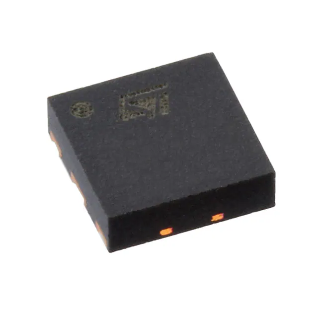
EMIF02-02OABRY
IPAD™ automotive grade integrated protected low pass filter for
BroadR Reach™ interface
Datasheet - production data
Description
The EMIF02-02OABRY is a highly integrated
solution designed to suppress EMI noise in
BroadR Reach™ interfaces in automotive
applications. This low pass filter includes a 15 kV
ISO10605 protection and is housed in a
3 x 3 mm² wettable flanks QFN.
Figure 1. EMIF02-02OABRY equivalent circuit
ϭ
ϲ
Ϯ
ϱ
ϯ
ϰ
Features
Attenuation profile compliant with
BroadR Reach™ requirements from -40 °C to
125 °C
Return loss (Sdd11) at 60 MHz: -20 dB
Components matching: 1% (between line 1
and 2)
Package:
– Dimensions: 3.0 x 3.0 mm
– Pitch: 1.1 µm
– Wettable flank QFN
AEC-Q101 compliant
Complies with the following standards
ISO 10605 (330 Ω / 330 pF) (pins 1 and 3):
– 15 kV (air discharge)
– 15 kV (contact discharge)
ISO 7637-3 (pins 1 and 3):
– Pulse 3a: -150 V
– Pulse 3b: +100 V
MIL-STD883J (HBM) (pins 4 and 6)
– ±2 kV
TM: IPAD is a trademark of STMicroelectronics.
June 2016
This is information on a product in full production.
DocID029487 Rev 1
1/11
www.st.com
�Characteristics
1
EMIF02-02OABRY
Characteristics
Table 1. Absolute ratings (Tamb = 25 °C)
Symbol
Parameter and test conditions
Value
Unit
External pins (pin 1 and pin 3):
IEC 61000-4-2 (330 Ω / 150 pF)
air discharge
contact discharge
±15
±15
External pins (pin 1 and pin 3):
ISO 10605 (330 Ω / 330 pF)
air discharge
contact discharge
±15
±15
VPP
Transceiver side pins: HBM (pin 4 and pin 6)
±2
kV
TL
Maximum lead temperature for soldering 10 s
260
°C
Top
Operating junction temperature range
-40 to +125
°C
Tstg
Storage temperature range
-55 to +125
°C
VPP
kV
Table 2. Electrical characteristics (Tamb = 25 °C)
Symbol
Conditions
Min.
VBR
Internal protection diode breakdown voltage,
IR = 20 mA
VCL
IPP = 1 A, 8/20 µs
RDC
Serial resistance (pins 3 to 4 or 1 to 6)
Typ.
6
Scd21
Sdc21
10.5
V
12
Ω
-20
-20
From 10 MHz to 60 MHz, Tj = -40 °C to 125 °C
-50
Figure 2. BroadR Reach application schematic
�
�
�
�
�
�
6GG��
2/11
Unit
V
Sdd11
Sdd22
Max.
DocID029487 Rev 1
6GG��
ddž
dB
�EMIF02-02OABRY
Characteristics
Figure 3. Sdd11 differential return loss curve -external pins
���
6GG�� �G%�
���&
��&
���&
���&
���
���
���
���
���
���
���
I�+]�
���
�(���
�(���
�(���
�(���
Figure 4. Sdd22 differential return loss curve -transceiver side pins
���
6GG���G%�
���&
���
��&
���&
���&
���
���
���
���
���
���
I�+]�
���
�(���
�(���
DocID029487 Rev 1
�(���
�(���
3/11
11
�Characteristics
EMIF02-02OABRY
Figure 5. Sdd21 attenuation curve
�
6GG���G%�
���&
��&
��
���&
���&
���
���
���
���
���
���
���
I�+]�
���
�(���
�(���
Figure 6. ESD response to ISO 10605C = 330 pF, R = 330 Ω (+15 kV contact)
��9�GLY
�(���
Figure 7. ESD response to ISO 10605C = 330 pF, R = 330 Ω (-15 kV contact)
��9�GLY
���QV�GLY
4/11
�(���
DocID029487 Rev 1
���QV�GLY
�EMIF02-02OABRY
Characteristics
Figure 8. Response to ISO 7637-3 (pulse 3a)
Us = -150 V
Figure 9. Response to ISO 7637-3 (pulse 3b)
Us = +100 V
��9�GLY
��9�GLY
����P$�GLY
����P$�GLY
���QV�GLY
DocID029487 Rev 1
���QV�GLY
5/11
11
�Package information
2
EMIF02-02OABRY
Package information
In order to meet environmental requirements, ST offers these devices in different grades of
ECOPACK® packages, depending on their level of environmental compliance. ECOPACK®
specifications, grade definitions and product status are available at: www.st.com.
ECOPACK® is an ST trademark.
2.1
QFN package information
Figure 10. QFN package outline
(
3,1���
,1'(;�$5($
723�9,(:
$�
$
6($7,1*
3/$1(
'K
$�
6,'(�9,(:
H
E
'�
�
�
/
'Z�
�
�
'Z�
%27720�9,(:
�
6/11
DocID029487 Rev 1
/�
�EMIF02-02OABRY
Package information
Table 3. QFN package mechanical data
Dimensions
Ref.
Inches(1)
Millimeters
Min.
Typ.
Max.
Min.
Typ.
Max.
A
0.80
0.85
0.90
0.0315
0.0335
0.0354
A1
0.00
0.02
0.05
0.00
0.0008
0.0020
A3
0.203
0.0080
b
0.45
0.50
0.55
0.0178
0.0197
0.0217
D
2.95
3.00
3.05
0.1161
0.1181
0.1201
E
2.95
3.00
3.05
0.1161
0.1181
0.1201
e
1.105
0.0436
L
0.85
0.90
0.95
0.0335
0.0354
0.0374
D2
0.60
0.70
0.80
0.0236
0.0276
0.0315
L1
0.07
0.15
0.23
0.0028
0.0060
0.0091
Dw1
0.30
0.35
0.40
0.0118
0.0138
0.0157
(2)
0.10
0.0217
0.0236
Dh
(2)
0.50
Dw2
0.0039
0.55
0.60
0.0197
1. Values in inches are converted from mm and rounded to 4 decimal digits.
2. Solder filled dimples
Figure 11. Footprint recommendations
(in mm)
Figure 12. Marking
�����
�����
ϭ
�����
�����
Ϯ
ϯ
^d
ϮϮ � Z z
ϳ � z t t
ϲ
ϱ
ϰ
�����
DocID029487 Rev 1
7/11
11
�Package information
EMIF02-02OABRY
Figure 13. Tape and reel outline
I��������������
I�
������� ����
����� ���
I��������������
I�
�������� ���
����� ����
�
������� ����
����
������ ���
^d
ϮϮ � Z z
ϳ � zt t
����
�
������� ���
6HFWLRQ�$�� $
8/11
����
8VHU�GLUHFWLRQ�RI�XQUHHOLQJ
DocID029487 Rev 1
�EMIF02-02OABRY
Recommendation on PCB assembly
3
Recommendation on PCB assembly
3.1
Reflow profile
Figure 14. ST ECOPACK® recommended soldering reflow profile for PCB mounting
��������&
7HPSHUDWXUH��&�
���
�� &�V
������&�V
�� VHF
��� PD[�
���
�� &�V
���
�� &�V
���
����&�V
��
7LPH��V�
�
Note:
��
��
��
���
���
���
���
���
���
���
Minimize air convection currents in the reflow oven to avoid component movement.
Maximum soldering profile corresponds to the latest IPC/JEDEC J-ST-020.
3.2
Stencil opening design
Figure 15. Recommended stencil window position in mm (inches)
�����
�����
�����
�����
�����
�����
�����
�����
�����
6WHQFLO�ZLQGRZ�RSHQLQJ
/HDG�IRRWSULQW�RQ�3&%
DocID029487 Rev 1
9/11
11
�Ordering information
4
EMIF02-02OABRY
Ordering information
Figure 16. Ordering information scheme
(0,)���������2$%5��<
(0,�)LOWHU
1XPEHU�RI�OLQHV
9HUVLRQ
2$%5��2SHQ�DOOLDQFH�%URDG5�5HDFK
很抱歉,暂时无法提供与“EMIF02-02OABRY”相匹配的价格&库存,您可以联系我们找货
免费人工找货