L5300GJ
Automotive 5 V low drop voltage regulator
Datasheet - production data
Programmable reset pulse delay with external
capacitor
Early warning
Very wide stability range with low value output
capacitor
Thermal shutdown and short circuit protection
PowerSSO-12
Wide temperature range (Tj = -40 °C to 150 °C)
Enable input for enabling / disabling the voltage
regulator
Features
Description
Max DC supply voltage
VS
40 V
Max output voltage tolerance
V0
+/-2%
Max dropout voltage
Vdp
500 mV
Output current
I0
300 mA
Quiescent current
Iqn
5 µA(1)
55 µA(2)
1. Typical value with regulator disabled.
L5300GJ is a low dropout linear regulator with
microprocessor control functions such as power
on reset, low voltage reset, early warning,
ON/OFF control. Typical quiescent current is 55
µA in very low output current mode and enabled
regulator. It drops to 5 µA with not enabled
regulator.
On-chip trimming results in high output voltage
accuracy (2%). Accuracy is kept over wide
temperature range, line and load variation. Early
warning circuit monitors the input voltage and
compares it with an internal voltage reference.
2. Typical value with regulator enabled.
AEC-Q100 qualified
Operating DC supply voltage
range
The maximum input voltage is 40 V. The
maximum output current is internally limited.
5.6 V to 40 V
Low dropout voltage
Internal temperature protection disables the
voltage regulator output. In addition, only low
value ceramic capacitor on output is required for
stability (equal or above 220 nF).
300 mA current capability
Low quiescent current
Very low consumption mode
Precision output voltage 5 V +/- 2%
Reset circuit sensing the output voltage
Table 1. Device summary
Order codes
Package
PowerSSO-12
September 2018
This is information on a product in full production.
Tube
Tape and reel
L5300GJ
L5300GJTR
DS6145 Rev 8
1/26
www.st.com
�Contents
L5300GJ
Contents
1
Block diagram and pins description . . . . . . . . . . . . . . . . . . . . . . . . . . . . 5
2
Electrical specifications . . . . . . . . . . . . . . . . . . . . . . . . . . . . . . . . . . . . . . 7
3
2.1
Absolute maximum ratings . . . . . . . . . . . . . . . . . . . . . . . . . . . . . . . . . . . . . 7
2.2
Thermal data . . . . . . . . . . . . . . . . . . . . . . . . . . . . . . . . . . . . . . . . . . . . . . . 7
2.3
Electrical characteristics . . . . . . . . . . . . . . . . . . . . . . . . . . . . . . . . . . . . . . . 8
2.4
Electrical characteristics curves . . . . . . . . . . . . . . . . . . . . . . . . . . . . . . . . 10
Application information . . . . . . . . . . . . . . . . . . . . . . . . . . . . . . . . . . . . . 14
3.1
Voltage regulator . . . . . . . . . . . . . . . . . . . . . . . . . . . . . . . . . . . . . . . . . . . 14
3.2
Reset . . . . . . . . . . . . . . . . . . . . . . . . . . . . . . . . . . . . . . . . . . . . . . . . . . . . 16
3.3
Early warning . . . . . . . . . . . . . . . . . . . . . . . . . . . . . . . . . . . . . . . . . . . . . . 16
3.4
Enable . . . . . . . . . . . . . . . . . . . . . . . . . . . . . . . . . . . . . . . . . . . . . . . . . . . 17
4
Package and PCB thermal data . . . . . . . . . . . . . . . . . . . . . . . . . . . . . . . 18
5
Package and packing information . . . . . . . . . . . . . . . . . . . . . . . . . . . . . 21
6
2/26
5.1
ECOPACK® . . . . . . . . . . . . . . . . . . . . . . . . . . . . . . . . . . . . . . . . . . . . . . . 21
5.2
PowerSSO-12 mechanical data . . . . . . . . . . . . . . . . . . . . . . . . . . . . . . . . 21
5.3
PowerSSO-12 packing information . . . . . . . . . . . . . . . . . . . . . . . . . . . . . 23
Revision history . . . . . . . . . . . . . . . . . . . . . . . . . . . . . . . . . . . . . . . . . . . 24
DS6145 Rev 8
�L5300GJ
List of tables
List of tables
Table 1.
Table 2.
Table 3.
Table 4.
Table 5.
Table 6.
Table 7.
Table 8.
Table 9.
Table 10.
Table 11.
Device summary . . . . . . . . . . . . . . . . . . . . . . . . . . . . . . . . . . . . . . . . . . . . . . . . . . . . . . . . . . 1
Pins description . . . . . . . . . . . . . . . . . . . . . . . . . . . . . . . . . . . . . . . . . . . . . . . . . . . . . . . . . . 6
Absolute maximum ratings . . . . . . . . . . . . . . . . . . . . . . . . . . . . . . . . . . . . . . . . . . . . . . . . . . 7
Thermal data. . . . . . . . . . . . . . . . . . . . . . . . . . . . . . . . . . . . . . . . . . . . . . . . . . . . . . . . . . . . . 7
General . . . . . . . . . . . . . . . . . . . . . . . . . . . . . . . . . . . . . . . . . . . . . . . . . . . . . . . . . . . . . . . . . 8
Reset . . . . . . . . . . . . . . . . . . . . . . . . . . . . . . . . . . . . . . . . . . . . . . . . . . . . . . . . . . . . . . . . . . 9
Early warning . . . . . . . . . . . . . . . . . . . . . . . . . . . . . . . . . . . . . . . . . . . . . . . . . . . . . . . . . . . . 9
Enable. . . . . . . . . . . . . . . . . . . . . . . . . . . . . . . . . . . . . . . . . . . . . . . . . . . . . . . . . . . . . . . . . . 9
PowerSSO-12 thermal parameter . . . . . . . . . . . . . . . . . . . . . . . . . . . . . . . . . . . . . . . . . . . 20
PowerSSO-12 mechanical data . . . . . . . . . . . . . . . . . . . . . . . . . . . . . . . . . . . . . . . . . . . . . 22
Document revision history . . . . . . . . . . . . . . . . . . . . . . . . . . . . . . . . . . . . . . . . . . . . . . . . . 24
DS6145 Rev 8
3/26
3
�List of figures
L5300GJ
List of figures
Figure 1.
Figure 2.
Figure 3.
Figure 4.
Figure 5.
Figure 6.
Figure 7.
Figure 8.
Figure 9.
Figure 10.
Figure 11.
Figure 12.
Figure 13.
Figure 14.
Figure 15.
Figure 16.
Figure 17.
Figure 18.
Figure 19.
Figure 20.
Figure 21.
Figure 22.
Figure 23.
Figure 24.
Figure 25.
Figure 26.
Figure 27.
Figure 28.
Figure 29.
Figure 30.
Figure 31.
Figure 32.
Figure 33.
Figure 34.
4/26
Block diagram . . . . . . . . . . . . . . . . . . . . . . . . . . . . . . . . . . . . . . . . . . . . . . . . . . . . . . . . . . . 5
Configuration diagram (top view) . . . . . . . . . . . . . . . . . . . . . . . . . . . . . . . . . . . . . . . . . . . . . 5
Output voltage vs Tj . . . . . . . . . . . . . . . . . . . . . . . . . . . . . . . . . . . . . . . . . . . . . . . . . . . . . . . . . . . . . . . . . . . . . 10
Output voltage vs VS. . . . . . . . . . . . . . . . . . . . . . . . . . . . . . . . . . . . . . . . . . . . . . . . . . . . . . 10
Output voltage vs VEn . . . . . . . . . . . . . . . . . . . . . . . . . . . . . . . . . . . . . . . . . . . . . . . . . . . . . 10
Drop voltage vs. output current. . . . . . . . . . . . . . . . . . . . . . . . . . . . . . . . . . . . . . . . . . . . . . 10
Current consumption vs. output current . . . . . . . . . . . . . . . . . . . . . . . . . . . . . . . . . . . . . . . 10
Current consumption vs. output current (at light load condition). . . . . . . . . . . . . . . . . . . . . 10
Current consumption vs input voltage (Io = 0.1 mA) . . . . . . . . . . . . . . . . . . . . . . . . . . . . . . 11
Current consumption vs input voltage (Io = 100 mA) . . . . . . . . . . . . . . . . . . . . . . . . . . . . . 11
Current limitation vs Tj . . . . . . . . . . . . . . . . . . . . . . . . . . . . . . . . . . . . . . . . . . . . . . . . . . . . 11
Current limitation vs input voltage. . . . . . . . . . . . . . . . . . . . . . . . . . . . . . . . . . . . . . . . . . . . 11
Short-circuit current vs Tj . . . . . . . . . . . . . . . . . . . . . . . . . . . . . . . . . . . . . . . . . . . . . . . . . . 11
Short-circuit current vs input voltage . . . . . . . . . . . . . . . . . . . . . . . . . . . . . . . . . . . . . . . . . 11
VEn_high vs Tj . . . . . . . . . . . . . . . . . . . . . . . . . . . . . . . . . . . . . . . . . . . . . . . . . . . . . . . . . . . 12
VEn_low vs Tj . . . . . . . . . . . . . . . . . . . . . . . . . . . . . . . . . . . . . . . . . . . . . . . . . . . . . . . . . . . . 12
VRhth vs Tj . . . . . . . . . . . . . . . . . . . . . . . . . . . . . . . . . . . . . . . . . . . . . . . . . . . . . . . . . . . . . . 12
VRlth vs Tj . . . . . . . . . . . . . . . . . . . . . . . . . . . . . . . . . . . . . . . . . . . . . . . . . . . . . . . . . . . . . . 12
VEWi_thh vs Tj . . . . . . . . . . . . . . . . . . . . . . . . . . . . . . . . . . . . . . . . . . . . . . . . . . . . . . . . . . . 12
VEWi_thl vs Tj . . . . . . . . . . . . . . . . . . . . . . . . . . . . . . . . . . . . . . . . . . . . . . . . . . . . . . . . . . . . 12
Icr vs Tj . . . . . . . . . . . . . . . . . . . . . . . . . . . . . . . . . . . . . . . . . . . . . . . . . . . . . . . . . . . . . . . . 13
Idr vs Tj . . . . . . . . . . . . . . . . . . . . . . . . . . . . . . . . . . . . . . . . . . . . . . . . . . . . . . . . . . . . . . . . 13
Application schematic . . . . . . . . . . . . . . . . . . . . . . . . . . . . . . . . . . . . . . . . . . . . . . . . . . . . . 14
Stability region . . . . . . . . . . . . . . . . . . . . . . . . . . . . . . . . . . . . . . . . . . . . . . . . . . . . . . . . . . 15
Maximum load variation response . . . . . . . . . . . . . . . . . . . . . . . . . . . . . . . . . . . . . . . . . . . 15
Reset time diagram. . . . . . . . . . . . . . . . . . . . . . . . . . . . . . . . . . . . . . . . . . . . . . . . . . . . . . . 16
Early warning time diagram . . . . . . . . . . . . . . . . . . . . . . . . . . . . . . . . . . . . . . . . . . . . . . . . 17
PowerSSO-12 PC board(1) . . . . . . . . . . . . . . . . . . . . . . . . . . . . . . . . . . . . . . . . . . . . . . . . . 18
Rthj-amb Vs. PCB copper area in open box free air condition . . . . . . . . . . . . . . . . . . . . . 18
PowerSSO-12 thermal impedance junction ambient single pulse . . . . . . . . . . . . . . . . . . . 19
Thermal fitting model of Vreg in in PowerSSO-12 . . . . . . . . . . . . . . . . . . . . . . . . . . . . . . . 19
PowerSSO-12 package dimensions . . . . . . . . . . . . . . . . . . . . . . . . . . . . . . . . . . . . . . . . . . 21
PowerSSO-12 tube shipment (no suffix) . . . . . . . . . . . . . . . . . . . . . . . . . . . . . . . . . . . . . . 23
PowerSSO-12 tape and reel shipment (suffix “TR”) . . . . . . . . . . . . . . . . . . . . . . . . . . . . . . 23
DS6145 Rev 8
�L5300GJ
1
Block diagram and pins description
Block diagram and pins description
Figure 1. Block diagram
Vo
Vs
START - UP
Vos
Pow er
En
VOLTAGE
Driver
REFERENCE
Thermal
Current
Shutdow n
limiter
Res
Low Voltage
Reset
Vcr
EWo
EWi
GND
Figure 2. Configuration diagram (top view)
TAB = Substrate
NC 1
12 EWo
Res 2
11 NC
Vcr 3
10 EWi
GND 4
9
En
Vos 5
8
NC
Vo 6
7
VS
DS6145 Rev 8
5/26
25
�Block diagram and pins description
L5300GJ
Table 2. Pins description
6/26
N°
Name
Function
1
NC
Not connected
2
Res
Reset output. Internally connected to Vo through a 20 K pull up
resistor. This pin is pulled low when Vo < Vo_th. Keep open if not
needed
3
Vcr
Reset delay. Connect an external capacitor between Vcr pin and
ground to adjust the reset delay time. Keep open if not needed
4
GND
5
Vos
Regulator output voltage sensing (connect to Vo)
6
Vo
5 V regulated output. Block to GND with a ceramic capacitor
(Co 220 nF for regulator stability)
7
VS
Supply voltage, block directly to GND on the IC with a capacitor
8
NC
Not connected
9
En
Enable input. A high signal switches the regulator ON. Connect to
VS if not needed
10
EWi
Early warning input. This pin monitors the VS voltage level through
a resistor divider. Connect to VS if not needed
11
NC
Not connected
12
EWo
Early warning output. Internally connected to Vo through 20 K
pull up resistor. This pin is pulled low when EWi is below bandgap
reference voltage. Keep open if not needed
-
TAB
TAB is connected to the substrate of the chip: connect to GND or
leave open (see Figure 2).
Ground reference
DS6145 Rev 8
�L5300GJ
Electrical specifications
2
Electrical specifications
2.1
Absolute maximum ratings
Stressing the device above the rating listed in the Table 3: Absolute maximum ratings may
cause permanent damage to the device. These are stress ratings only and operation of the
device at these or any other conditions above those indicated in the operating sections of
this specification is not implied. Exposure to absolute maximum rating conditions for
extended periods may affect device reliability.
Table 3. Absolute maximum ratings
Symbol
Unit
-0.3 to 40
V
DC supply voltage
IVsdc
Input current
Vodc
DC output voltage
-0.3 to 6
IVodc
DC output current
Internally limited
Vod Res
Open drain output voltage Res
-0.3 to Vodc + 0.3
Iod Res
Open drain output current Res
Internally limited
Vod EWo
Open drain output voltage EWo
-0.3 to Vodc + 0.3
Iod EWo
Open drain output current EWo
Internally limited
Vcr voltage
-0.3 to Vo + 0.3
V
Internally limited
V
V
V
VEWi
Early warning input voltage
-0.3 to 40
V
VEn
Enable input
-0.3 to 40
V
Junction temperature
-40 to 150
°C
Tj
VESD HBM
ESD HBM voltage level (HBM-MIL STD 883C)
+/- 2
kV
VESD CDM
ESD CDM voltage level (CDM AEC-Q100-011)
+/- 750
V
Thermal data
m
Table 4. Thermal data
Symbol
Note:
Value
Vsdc
Vcr
2.2
Parameter
Parameter
Value
Unit
Rthj-case
Thermal resistance junction to case: PowerSSO-12
8
°K/W
Rthj-amb
Thermal resistance junction to ambient: PowerSSO-12
48
°K/W
The values quoted are for PCB 77mm x 86 mm x 1.6mm, FR4, double layer with thermal
vias (one copper heatsink layer, thickness 0.070 mm, area 8 cm2).
DS6145 Rev 8
7/26
25
�Electrical specifications
2.3
L5300GJ
Electrical characteristics
Values specified in this section are for VS = 5.6 V to 31 V, Tj = -40°C to 150°C unless
otherwise stated.
Table 5. General
Pin
Symbol
Vo
Vo_ref
Output voltage
VS = 8 V to 18 V;
Io = 8 mA to 300 mA
4.9
Vo
Vo_ref
Output voltage
VS = 5.6 V to 31V;
Io = 8 mA to 300 mA
Vo
Vo_ref
Output voltage
Vo
Ishort
Short circuit current
Vo
Ilim
VS, Vo
Vline
Vo
Vload
Parameter
Output current
capability(1)
Line regulation voltage
Load regulation voltage
Test condition
Min. Typ.
Max.
Unit
5.0
5.1
V
4.85
5.0
5.15
V
VS = 5.6 V to 31 V;
Io = 0.1 mA to 8 mA
4.75
5.0
5.25
V
VS = 13.5 V
0.8
1.8
2.6
A
VS = 13.5 V
0.6
1.6
2.5
A
VS = 6 V to 28 V;
Io = 60 mA
40
mV
VS = 13.5 V;
Io = 8 mA to 300 mA;
Tj = 25 °C
40
VS = 8 V to 18 V;
Io = 8 mA to 300 mA
55
500
mV
VS, Vo
Vdp
Drop voltage (2)
Io = 300 mA
VS, Vo
SVR
Ripple rejection
fr = 100 Hz (3)
Vo
Ioth_H
Normal consumption mode
output current
Vo
Ioth_L
Very low consumption
mode output current
Vo
Ioth_Hyst
Output current switching
threshold hysteresis
VS = 13.5 V; Tj = 25 °C
VS, Vo
Iqs
Current consumption with
regulator disabled
Iqs = IVs – Io
VS = 13.5 V; En = low
5
10
µA
VS, Vo
Iqn_1
Current consumption with
regulator enabled
Iqn_1 = IVs – Io
VS = 13.5 V;
Io = 0.1 mA to 1mA;
En = high
55
80
µA
VS, Vo
Iqn_300
Current consumption with
regulator enabled
Iqn_300 = IVs – Io
VS = 13.5 V;
Io = 300 mA; En = high
3
4.2
mA
190
°C
Tw
Tw_hy
60
dB
8
mA
1.1
Thermal protection
temperature
Thermal protection
temperature hysteresis
mV
0.8
150
10
mA
mA
°C
1. Measured output current when the output voltage has dropped 100 mV from its nominal value obtained at
13.5 V and Io = 75 mA.
8/26
DS6145 Rev 8
�L5300GJ
Electrical specifications
2. VS - Vo measured dropout when the output voltage has dropped 100 mV from its nominal value obtained
at 13.5V and Io = 75 mA.
3. Guaranteed by design.
Table 6. Reset
Pin
Symbol
Parameter
Test condition
Min.
Res
VRes_l
Reset output low voltage
Res
IRes_lkg
Reset output high leakage
VRes = Vout
current
Res
Rres
Pull-up internal resistance Versus Vo
10
Res
Vo_th
Vo out of regulation
threshold
Vcr
VRlth
Vcr
VRhth
Vcr
Typ.
Max.
Unit
0.4
V
1
µA
20
40
k
6
8
10
%below
Vo_ref
Reset timing low threshold VS = 13.5 V
15
18
22
% Vo_ref
Reset timing high
threshold
VS = 13.5 V
47
50
53
% Vo_ref
Icr
Charge current
VS = 13.5 V
10
20
30
µA
Vcr
Idr
Discharge current
VS = 13.5 V
10
20
30
µA
Res
Trr
Reset reaction time
2
µs
Res
Trd
Reset delay time
6
ms
Rext = 5 k; Vo > 1 V
Vo decreasing
VS = 13.5 V; Ctr = 1 nF
2
4
Table 7. Early warning
Pin
Symbol
EWi
Ewi_th_low
EWi
Parameter
Test condition
Min.
Typ.
Max.
Unit
EW input low threshold
voltage
2.35
2.50
2.65
V
Ewi_th_high
EW input high threshold
voltage
2.42
2.57
2.72
V
EWi
Ewi_th_hyst
EW input threshold
hysteresis
EWi
IEWi_lkg
EW input leakage current VEWi = 0 V; VS > 3 V
-1
EWo
REWo
Pull-up internal resistance Versus Vo
10
EWo
EWo_lv
EW output low voltage
(with external pull up)
VEWi < 2.35 V;
VS > 4 V; Rext = 5 k
EWo
IWo
EW output leakage
VEWo = 5 V
70
20
mV
1
µA
40
k
400
mV
1
µA
Table 8. Enable
Pin
Symbol
Parameter
En
VEn_low
En input low voltage
En
VEn_high
En input high voltage
En
VEn_hyst
En input hysteresis
En
I_leak
Pull-down current
Test condition
Min.
Typ.
Max.
Unit
1
V
3
V
500
VEn = 5 V
DS6145 Rev 8
3
mV
10
µA
9/26
25
�Electrical specifications
2.4
L5300GJ
Electrical characteristics curves
Figure 3. Output voltage vs Tj
9RBUHI�9�
���
���
���
���
���
���
���
���
���
���
���
��� ���
Figure 4. Output voltage vs VS
9RBUHI�9�
�
�
9V� �����9
,R� ���P$
�
7F ��&
,R� ���P$
�
�
��
�
�� ��
�
�� ��� ��� ��� ���
7M�&�
�
�
�
�
�
�
�
9V�9�
*$3*&)7�����
Figure 5. Output voltage vs VEn
�
��
*$3*&)7�����
Figure 6. Drop voltage vs. output current
9RBUHI�9�
9GS�9�
���
���
���
9V� �����9
7F� ���&
���
���
���
7L ���&
���
�
���
���
���
���
���
���
���
7L ��&
��
�
�
����
�
���
���
���
���
�
���
���
9HQ�9�
�
���
���
*$3*&)7�����
��
���
���
���
���
���
,R�P$�
Figure 7. Current consumption vs. output
current
���
*$3*&)7�����
Figure 8. Current consumption vs. output
current (at light load condition)
,TQ�P$�
,TQ�P$�
���
�
�
���
���
�
���
�
�
���
���
�
�9V� �����9
(Q� �+LJK
7M� ���&
�
���
�9V� �����9
(Q� �+LJK
���
�
�
���
���
�
�
�
��
���
���
���
,R�P$�
10/26
���
���
���
����
�
*$3*&)7�����
DS6145 Rev 8
�
�
�
�
�
,R�P$�
�
�
�
�
��
*$3*&)7�����
�L5300GJ
Electrical specifications
Figure 9. Current consumption vs input voltage
(Io = 0.1 mA)
,TQ�$�
Figure 10. Current consumption vs input
voltage (Io = 100 mA)
,TQ�P$�
���
���
���
���
���
���
���
���
���
���
���
���
���
���
(Q� �+LJK
7M ��&
���
���
���
��
��
��
��
�
�
�
�
��
��
��
��
��
,R�P$�
��
��
��
(Q� �+LJK
7M ��&
�
�
�
��
��
*$3*&)7�����
Figure 11. Current limitation vs Tj
��
��
��
��
,R�P$�
��
��
*$3*&)7�����
Figure 12. Current limitation vs input voltage
,OLP�P$�
,OLP�P$�
����
����
����
����
����
����
����
����
���
���
�
9V� �����9
���
���
�
��
��
��
��� ��� ��� ���
7M�&�
7M� ���&
7M� ����&
�
*$3*&)7�����
Figure 13. Short-circuit current vs Tj
�
�
��
��
��
��
9V�9�
��
*$3*&)7�����
Figure 14. Short-circuit current vs input voltage
,VKRUW�P$�
,VKRUW�P$�
����
����
����
����
����
����
����
9V� �����9
����
����
����
����
���
���
��� ���
����
����
����
����
����
����
���
���
���
���
�
�
��
��
�� ��� ��� ��� ���
7M�&�
7M� ���&
����
����
����
���
���
���
*$3*&)7�����
DS6145 Rev 8
7M� ����&
�
�
�
��
��
9V�9�
��
��
��
*$3*&)7�����
11/26
25
�Electrical specifications
L5300GJ
Figure 15. VEn_high vs Tj
Figure 16. VEn_low vs Tj
9HQBKLJK�9�
9HQBORZ �9�
���
���
���
���
���
���
���
���
���
���
���
���
���
���
���
���
���
���
���
���
���
���
9V� ������9�WR����9
���
���
�
��
��
��
9V� ����9�WR���9
���
��� ��� ��� ���
���
�
��
��
��
��� ��� ��� ���
7M�&�
7M�&�
*$3*&)7�����
*$3*&)7�����
Figure 17. VRhth vs Tj
Figure 18. VRlth vs Tj
9UKWK��9RBUHI�
9UOWK��9RBUHI�
��
��
��
��
��
��
��
��
��
��
��
9V� ����9�WR���9
���
���
�
��
��
��
��� ��� ��� ���
7M�&�
��
��
��
��
��
��
��
�
�
�
�
9V� ����9�WR���9
���
*$3*&)7�����
���
�
��
��
��
��� ��� ��� ���
7M�&�
Figure 19. VEWi_thh vs Tj
Figure 20. VEWi_thl vs Tj
9HZLBWKO�9�
9HZLBWKK�9�
���
���
���
���
���
���
���
���
���
���
���
���
���
���
���
���
���
���
���
���
���
���
9V� ����9�WR���9
���
���
�
��
��
��
7M�&�
12/26
*$3*&)7�����
��� ��� ��� ���
9V� ����9�WR���9
���
*$3*&)7�����
DS6145 Rev 8
���
�
��
��
��
7M�&�
��� ��� ��� ���
*$3*&)7�����
�L5300GJ
Electrical specifications
Figure 21. Icr vs Tj
Figure 22. Idr vs Tj
,FU�$�
,GU�$�
��
��
��
��
��
��
��
��
��
�
�
��
��
��
��
��
��
��
��
��
�
�
9V� ����9�WR���9
���
���
�
��
��
��
7M�&�
��� ��� ��� ���
9V� ����9�WR���9
���
*$3*&)7�����
DS6145 Rev 8
���
�
��
��
��
7M�&�
��� ��� ��� ���
*$3*&)7�����
13/26
25
�Application information
L5300GJ
3
Application information
3.1
Voltage regulator
The voltage regulator uses a p-channel mos transistor as a regulating element. With this
structure a very low dropout voltage at current up to 300 mA is obtained. The output voltage
is regulated up to input supply voltage of 40 V. The high-precision of the output voltage (2%)
is obtained with a pre-trimmed reference voltage. The voltage regulator automatically
adapts its own quiescent current to the output current level. In light load conditions the
quiescent current goes down to 55 µA only (low consumption mode). This procedure
features a certain hysteresis on the output current (see Figure ). Short-circuit protection to
GND and a thermal shutdown are provided.
Figure 23. Application schematic
9%$77
9R
9V
567
&�
&�
(Q
5�(:
5�
/����*9FU
(:L
(:R
5�
5�(:
*1'
("1($'5�����
The input capacitor C1 100 µF is necessary as backup supply for negative pulses which
may occur on the line. The second input capacitor C2 220 nF is needed when the C1 is too
distant from the VS pin and it compensates smooth line disturbances. The C0 ceramic
capacitor, connected to the output pin, is for bypassing to GND the high-frequency noise
and it guarantees stability even during sudden line and load variations. Suggested value is
C0 = 220 nF?with ESR 100 m.
Stability region is reported in Figure 24.
14/26
DS6145 Rev 8
�L5300GJ
Application information
Figure 24. Stability region
����
(65��2KP��
���
��
67$%,/,7
很抱歉,暂时无法提供与“L5300GJTR”相匹配的价格&库存,您可以联系我们找货
免费人工找货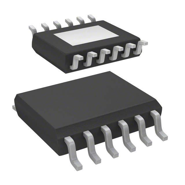


 工商网监
湘ICP备2023018690号
工商网监
湘ICP备2023018690号
