STGB20NB32LZ
STGB20NB32LZ-1
N-CHANNEL CLAMPED 20A - D2PAK/I2PAK
INTERNALLY CLAMPED PowerMESH™ IGBT
TYPE
VCES
VCE(sat)
IC
STGB20NB32LZ
STGB20NB32LZ-1
CLAMPED
CLAMPED
< 2.0 V
< 2.0 V
20 A
20 A
POLYSILICON GATE VOLTAGE DRIVEN
LOW THRESHOLD VOLTAGE
LOW ON-VOLTAGE DROP
HIGH CURRENT CAPABILITY
HIGH VOLTAGE CLAMPING FEATURE
)
s
(
t
c
u
d
o
)
r
s
(
P
t
c
e
t
u
e
d
l
o
o
r
s
P
b
e
O
t
e
l
)
o
s
(
s
t
b
c
u
O
d
o
)
r
s
P
(
t
c
e
t
u
e
l
d
o
o
r
s
P
b
O
e
t
e
l
o
s
b
O
■
■
■
■
■
3
3
12
1
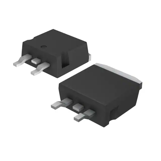
D 2PAK
I2PAK
DESCRIPTION
Using the latest high voltage technology based on a
patented strip layout, STMicroelectronics has
designed an advanced family of IGBTs, the
PowerMESH™ IGBTs, with outstanding
performances. The built in collector-gate zener
exhibits a very precise active clamping while the
gate-emitter zener supplies an ESD protection.
INTERNAL SCHEMATIC DIAGRAM
APPLICATIONS
■ ELECTRONIC IGNITION FOR AUTOMOTIVE
ORDERING INFORMATION
SALES TYPE
MARKING
PACKAGE
PACKAGING
STGB20NB32LZT4
GB20NB32LZ
D2PAK
TAPE & REEL
STGB20NB32LZ-1
GB20NB32LZ
I2PAK
TUBE
December 2003
1/11
�STGB20NB32LZ - STGB20NB32LZ-1
ABSOLUTE MAXIMUM RATINGS
Symbol
Parameter
VCES
Collector-Emitter Voltage (VGS = 0)
VECR
Reverse Battery Protection
VGE
Gate-Emitter Voltage
Value
Unit
CLAMPED
V
20
V
CLAMPED
V
IC
Collector Current (continuous) at Tc = 25°C
40
A
IC
Collector Current (continuous) at Tc = 100°C
30
A
Collector Current (pulsed)
80
A
Eas
Single Pulse Energy Tc = 25°C
700
mJ
Ptot
Total Dissipation at Tc = 25°C
ICM (�)
150
W
Derating Factor
1
W/°C
ESD
ESD (Human Body Model)
4
KV
Tstg
Storage Temperature
–65 to 175
°C
175
°C
)
s
(
t
c
u
d
o
)
r
s
(
P
t
c
e
t
u
e
d
l
o
o
r
s
P
b
e
O
t
e
l
)
o
s
(
s
t
b
c
u
O
d
o
)
r
s
P
(
t
c
e
t
u
e
l
d
o
o
r
s
P
b
O
e
t
e
l
o
s
b
O
Tj
Max. Operating Junction Temperature
(•)Pulse width limited by safe operating area
THERMAL DATA
Rthj-case
Thermal Resistance Junction-case Max
Rthj-amb
Thermal Resistance Junction-ambient Max
1
°C/W
62.5
°C/W
ELECTRICAL CHARACTERISTICS (TCASE = 25 °C UNLESS OTHERWISE SPECIFIED)
OFF
Symbol
Parameter
Test Conditions
Min.
Typ.
Max.
Unit
IC = 2 mA, VGE = 0, Tc= - 40°C
330
355
380
V
IC = 2 mA, VGE = 0, Tc= 25°C
325
350
375
V
IC = 2 mA, VGE = 0, Tc= 150°C
320
345
370
V
Emitter Collector Break-down
Voltage
IC = 75 mA, Tc = 25°C
20
28
BVGE
Gate Emitter Break-down
Voltage
IG = ± 2 mA
12
14
ICES
Collector cut-off Current
(VGE = 0)
VCE = 15 V, VGE =0 ,TC =150 °C
10
µA
VCE =200 V, VGE=0 ,TC =150°C
100
µA
BV(CES)
BV(ECR)
Clamped Voltage
IGES
Gate-Emitter Leakage
Current (VCE = 0)
RGE
Gate Emitter Resistance
VGE = ± 10V , VCE = 0
V
16
V
± 400
± 660
± 1000
10
15
25
KΩ
Test Conditions
Min.
Typ.
Max.
Unit
VCE = VGE, IC = 250µA, Tc=-40°C
1.2
VCE = VGE, IC = 250µA, Tc= 25°C
1
VCE =VGE, IC = 250µA, Tc=150°C
0.6
µA
ON (1)
Symbol
VGE(th)
VCE(SAT)
2/11
Parameter
Gate Threshold Voltage
Collector-Emitter Saturation
Voltage
V
V
1.4
2
VGE =4.5V, IC = 10 A, Tc= 25°C
1.1
1.8
V
VGE =4.5V, IC = 10 A, Tc= 150°C
1
1.7
V
VGE =4.5V, IC = 20 A, Tc= 25°C
1.35
2
V
VGE =4.5V, IC = 20 A, Tc= 150°C
1.25
2
V
V
�STGB20NB32LZ - STGB20NB32LZ-1
ELECTRICAL CHARACTERISTICS (TCASE = 25 °C UNLESS OTHERWISE SPECIFIED)
DYNAMIC
Symbol
gfs
Parameter
Forward Transconductance
Cies
Input Capacitance
Coes
Output Capacitance
Cres
Reverse Transfer
Capacitance
Qg
Gate Charge
Test Conditions
Min.
VCE = 25 V , IC =20 A
VCE = 25 V, f = 1 MHz, VGE = 0
VCE = 280 V, IC = 20 A,
VGE = 5 V
Typ.
Max.
Unit
35
S
2300
pF
165
pF
28
pF
51
nC
)
s
(
t
c
u
d
o
)
r
s
(
P
t
c
e
t
u
e
d
l
o
o
r
s
P
b
e
O
t
e
l
)
o
s
(
s
t
b
c
u
O
d
o
)
r
s
P
(
t
c
e
t
u
e
l
d
o
o
r
s
P
b
O
e
t
e
l
o
s
b
O
FUNCTIONAL CHARACTERISTICS
Symbol
II
U.I.S.
Parameter
Test Conditions
Min.
Typ.
Max.
Unit
34
A
RGOFF =1KΩ ,Tc=125°C, VG = 5 V,
L = 1.6mH
21.6
A
Test Conditions
Min.
Latching Current
RGOFF =127Ω, VClamp = 250 V,
VGE = 5 V, TC = 125 °C
Functional Test Open
Secondary Coil
SWITCHING ON
Symbol
td(on)
tr
(di/dt)on
Eon
Parameter
Typ.
Max.
Unit
Delay Time
Rise Time
VCC = 250 V, IC = 20 A
RG = 1KΩ , VGE = 4.5 V
2.3
0.6
µs
µs
Turn-on Current Slope
VCC= 250 V, IC = 20 A
RG=1KΩ, VGE = 4.5 V
550
A/µs
Turn-on Switching Losses
VCC= 250 V, IC = 20 A, Tc=25°C
RG=1KΩ, VGE = 4.5 V, Tc=150°C
8.8
9.2
mJ
mJ
SWITCHING OFF
Symbol
tc
tr(Voff)
tf
td(off)
Eoff(**)
tc
tr(Voff)
tf
Parameter
Cross-Over Time
Off Voltage Rise Time
Test Conditions
Vcc = 250 V, IC = 20 A,
RGE = 1 KΩ , VGE = 4.5 V
Fall Time
Off Voltage Delay Time
Turn-off Switching Loss
Cross-Over Time
Off Voltage Rise Time
Fall Time
Vcc = 250 V, IC = 20 A,
RGE = 1 KΩ , VGE = 4.5 V
Tc = 150 °C
Min.
Typ.
Max.
Unit
4.8
µs
2.6
µs
2
µs
11.5
µs
11.8
mJ
7.8
µs
3.5
µs
3.9
µs
td(off)
Off Voltage Delay Time
12
µs
Eoff(**)
Turn-off Switching Loss
17.8
mJ
(**)Losses Include Also the Tail (jedec Standardization)
3/11
�STGB20NB32LZ - STGB20NB32LZ-1
Output Characteristics
Transfer Characteristics
)
s
(
t
c
u
d
o
)
r
s
(
P
t
c
e
t
u
e
d
l
o
o
r
s
P
b
e
O
t
e
l
)
o
s
(
s
t
b
c
u
O
d
o
)
r
s
P
(
t
c
e
t
u
e
l
d
o
o
r
s
P
b
O
e
t
e
l
o
s
b
O
Normalized Gate Threshold Voltage vs Temp.
Transconductance
Collector-Emitter On Voltage vs Temperature
Capacitance Variations
4/11
�STGB20NB32LZ - STGB20NB32LZ-1
Gate Charge vs Gate-Emitter Voltage
Normalized BreakDown Voltage vs Temperature
)
s
(
t
c
u
d
o
)
r
s
(
P
t
c
e
t
u
e
d
l
o
o
r
s
P
b
e
O
t
e
l
)
o
s
(
s
t
b
c
u
O
d
o
)
r
s
P
(
t
c
e
t
u
e
l
d
o
o
r
s
P
b
O
e
t
e
l
o
s
b
O
Break-Down Voltage vs Emitter Resistance
BVGEO (Zener Gate-Emitter) vs Temperature
Self Clamped Inductive Switching Energy vs
Open Secondary Coil
dV/dt Gate-Emitter Resistance
5/11
�STGB20NB32LZ - STGB20NB32LZ-1
BVEC Reverse Battery Voltage
Thermal Impedance
)
s
(
t
c
u
d
o
)
r
s
(
P
t
c
e
t
u
e
d
l
o
o
r
s
P
b
e
O
t
e
l
)
o
s
(
s
t
b
c
u
O
d
o
)
r
s
P
(
t
c
e
t
u
e
l
d
o
o
r
s
P
b
O
e
t
e
l
o
s
b
O
Switching Off Safe Operating Area
6/11
�STGB20NB32LZ - STGB20NB32LZ-1
Fig. 1: Unclamped Inductive Load Test Circuit
Fig. 2: Unclamped Inductive Waveform
)
s
(
t
c
u
d
o
)
r
s
(
P
t
c
e
t
u
e
d
l
o
o
r
s
P
b
e
O
t
e
l
)
o
s
(
s
t
b
c
u
O
d
o
)
r
s
P
(
t
c
e
t
u
e
l
d
o
o
r
s
P
b
O
e
t
e
l
o
s
b
O
Fig. 3: Test Circuit For Inductive Load Switching
And Diode Recovery Times
Fig. 4: Gate Charge test Circuit
7/11
�STGB20NB32LZ - STGB20NB32LZ-1
D2PAK MECHANICAL DATA
mm.
inch
DIM.
MIN.
TYP
MAX.
MIN.
TYP.
MAX.
A
4.4
4.6
0.173
0.181
A1
2.49
2.69
0.098
0.106
A2
0.03
0.23
0.001
0.009
B
0.7
0.93
0.027
0.036
B2
1.14
1.7
0.044
0.067
C
0.45
0.6
0.017
0.023
C2
1.23
1.36
0.048
0.053
D
8.95
9.35
0.352
0.368
)
s
(
t
c
u
d
o
)
r
s
(
P
t
c
e
t
u
e
d
l
o
o
r
s
P
b
e
O
t
e
l
)
o
s
(
s
t
b
c
u
O
d
o
)
r
s
P
(
t
c
e
t
u
e
l
d
o
o
r
s
P
b
O
e
t
e
l
o
s
b
O
D1
E
8
0.315
10
E1
10.4
0.393
8.5
0.334
G
4.88
5.28
0.192
0.208
L
15
15.85
0.590
0.625
L2
1.27
1.4
0.050
0.055
L3
1.4
1.75
0.055
0.068
M
2.4
3.2
0.094
0.126
R
0.015
0º
8º
3
V2
0.4
8/11
1
�STGB20NB32LZ - STGB20NB32LZ-1
TO-262 (I2PAK) MECHANICAL DATA
mm.
inch
DIM.
MIN.
TYP
MAX.
MIN.
TYP.
MAX.
A
4.40
4.60
0.173
0.181
A1
2.40
2.72
0.094
0.107
b
0.61
0.88
0.024
0.034
b1
1.14
1.70
0.044
0.066
)
s
(
t
c
u
d
o
)
r
s
(
P
t
c
e
t
u
e
d
l
o
o
r
s
P
b
e
O
t
e
l
)
o
s
(
s
t
b
c
u
O
d
o
)
r
s
P
(
t
c
e
t
u
e
l
d
o
o
r
s
P
b
O
e
t
e
l
o
s
b
O
c
0.49
0.70
0.019
0.027
c2
1.23
1.32
0.048
0.052
D
8.95
9.35
0.352
0.368
e
2.40
2.70
0.094
0.106
e1
4.95
5.15
0.194
0.202
E
10
10.40
0.393
0.410
L
13
14
0.511
0.551
L1
3.50
3.93
0.137
0.154
L2
1.27
1.40
0.050
0.055
9/11
�STGB20NB32LZ - STGB20NB32LZ-1
D2PAK FOOTPRINT
TUBE SHIPMENT (no suffix)*
)
s
(
t
c
u
TAPE AND REEL SHIPMENT (suffix ”T4”)* d
o
)
r
s
(
P
t
c
e
t
u
e
d
l
o
o
r
s
P
b
e
O
t
e
l
)
o
s
(
s
t
b
c
u
O
d
o
)
r
s
P
(
t
c
e
t
u
e
l
d
o
o
r
s
P
b
O
e
t
e
l
o
s
b
O
REEL MECHANICAL DATA
DIM.
mm
MIN.
A
B
DIM.
mm
MIN.
inch
MAX.
MIN.
MAX.
A0
10.5
10.7
0.413 0.421
B0
15.7
15.9
0.618 0.626
D
1.5
1.6
0.059 0.063
D1
1.59
1.61
0.062 0.063
E
1.65
1.85
0.065 0.073
F
11.4
11.6
0.449 0.456
K0
4.8
5.0
0.189 0.197
P0
3.9
4.1
0.153 0.161
P1
11.9
12.1
0.468 0.476
P2
1.9
2.1
0.075 0.082
R
50
1.574
T
0.25
0.35 0.0098 0.0137
W
23.7
24.3
* on sales type
10/11
0.933 0.956
inch
MIN.
330
1.5
C
12.8
D
20.2
G
24.4
N
100
T
TAPE MECHANICAL DATA
MAX.
MAX.
12.992
0.059
13.2
0.504 0.520
0795
26.4
0.960 1.039
3.937
30.4
1.197
BASE QTY
BULK QTY
1000
1000
�STGB20NB32LZ - STGB20NB32LZ-1
)
s
(
t
c
u
d
o
)
r
s
(
P
t
c
e
t
u
e
d
l
o
o
r
s
P
b
e
O
t
e
l
)
o
s
(
s
t
b
c
u
O
d
o
)
r
s
P
(
t
c
e
t
u
e
l
d
o
o
r
s
P
b
O
e
t
e
l
o
s
b
O
Information furnished is believed to be accurate and reliable. However, STMicroelectronics assumes no responsibility for the
consequences of use of such information nor for any infringement of patents or other rights of third parties which may result from
its use. No license is granted by implication or otherwise under any patent or patent rights of STMicroelectronics. Specifications
mentioned in this publication are subject to change without notice. This publication supersedes and replaces all information
previously supplied. STMicroelectronics products are not authorized for use as critical components in life support devices or
systems without express written approval of STMicroelectronics.
© The ST logo is a registered trademark of STMicroelectronics
© 2003 STMicroelectronics - Printed in Italy - All Rights Reserved
STMicroelectronics GROUP OF COMPANIES
Australia - Brazil - Canada - China - Finland - France - Germany - Hong Kong - India - Israel - Italy - Japan - Malaysia - Malta - Morocco
Singapore - Spain - Sweden - Switzerland - United Kingdom - United States.
© http://www.st.com
11/11
�