STGW25H120DF2, STGWA25H120DF2
Datasheet
Trench gate field-stop IGBT, H series 1200 V, 25 A high speed
Features
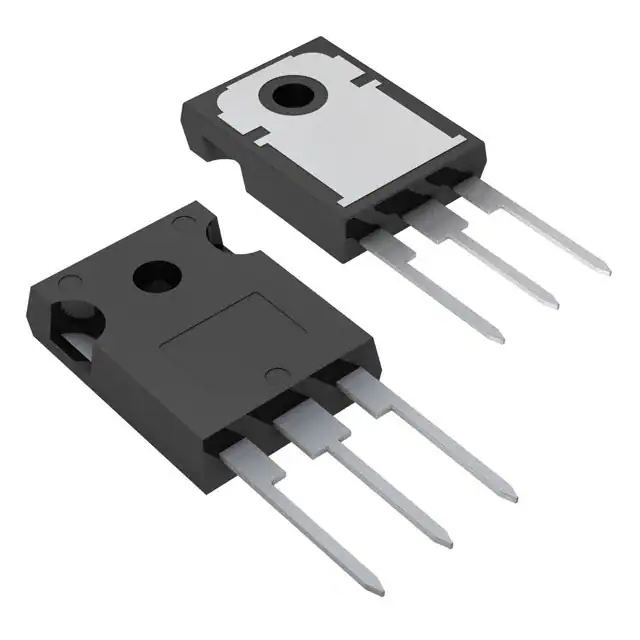
1
TO-247
2
3
1
2
3
TO-247 long leads
•
Maximum junction temperature: TJ = 175 °C
•
•
•
High speed switching series
Minimized tail current
VCE(sat) = 2.1 V (typ.) @ IC = 25 A
•
5 μs minimum short circuit withstand time at TJ = 150 °C
•
•
•
Safe paralleling
Low thermal resistance
Very fast recovery antiparallel diode
Applications
•
•
•
•
•
Photovoltaic inverters
Uninterruptible power supply
Welding
Power factor correction
High frequency converters
Description
This device is an IGBT developed using an advanced proprietary trench gate fieldstop structure. The device is part of the H series of IGBTs, which represents an
optimum compromise between conduction and switching losses to maximize the
efficiency of high-switching frequency converters. Furthermore, a slightly positive
VCE(sat) temperature coefficient and very tight parameter distribution result in safer
paralleling operation.
Product status links
STGW25H120DF2
STGWA25H120DF2
Product summary
Order code
STGW25H120DF2
Marking
G25H120DF2
Package
TO-247
Packing
Tube
Order code
STGWA25H120DF2
Marking
G25H120DF2
Package
TO-247 long leads
Packing
Tube
DS9297 - Rev 5 - March 2021
For further information contact your local STMicroelectronics sales office.
www.st.com
�STGW25H120DF2, STGWA25H120DF2
Electrical ratings
1
Electrical ratings
Table 1. Absolute maximum ratings
Symbol
VCES
Parameter
Collector-emitter voltage (VGE = 0 V)
Value
Unit
1200
V
Continuous collector current at TC = 25 °C
50
Continuous collector current at TC = 100 °C
25
Pulsed collector current
100
Gate-emitter voltage
±20
Transient gate-emitter voltage (tp ≤ 10 μs, D ≤ 0.01)
±30
Continuous forward current at TC = 25 °C
50
Continuous forward current at TC = 100 °C
25
IFP(1)
Pulsed forward current
100
A
PTOT
Total power dissipation at TC = 25 °C
375
W
TJ
Operating junction temperature range
- 55 to 175
°C
Storage temperature range
- 55 to 150
°C
Value
Unit
IC
ICP(1)
VGE
IF
TSTG
A
A
V
A
1. Pulse width limited by maximum junction temperature.
Table 2. Thermal data
Symbol
RthJC
RthJA
DS9297 - Rev 5
Parameter
Thermal resistance, junction-to-case IGBT
0.4
Thermal resistance, junction-to-case diode
1.47
Thermal resistance, junction-to-ambient
50
°C/W
°C/W
page 2/17
�STGW25H120DF2, STGWA25H120DF2
Electrical characteristics
2
Electrical characteristics
TJ = 25 °C unless otherwise specified.
Table 3. Static characteristics
Symbol
Parameter
Test conditions
V(BR)CES
Collector-emitter breakdown
voltage
VCE(sat)
Collector-emitter saturation
voltage
VF
Forward on-voltage
VGE = 0 V, IC = 2 mA
Min.
Typ.
1200
2.1
VGE = 15 V, IC = 25 A, TJ = 125 °C
2.4
VGE = 15 V, IC = 25 A, TJ = 175 °C
2.5
IF = 25 A
3.8
IF = 25 A, TJ = 125 °C
3.05
IF = 25 A, TJ = 175 °C
2.8
Gate threshold voltage
VCE = VGE, IC = 1 mA
ICES
Collector cut-off current
IGES
Gate-emitter leakage current
5
Unit
V
VGE = 15 V, IC = 25 A
VGE(th)
Max.
6
2.6
V
4.9
V
7
V
VGE = 0 V, VCE = 1200 V
25
µA
VCE = 0 V, VGE = ±20 V
250
nA
Table 4. Dynamic characteristics
Symbol
DS9297 - Rev 5
Parameter
Cies
Input capacitance
Coes
Output capacitance
Cres
Reverse transfer capacitance
Qg
Total gate charge
Qge
Gate-emitter charge
Qgc
Gate-collector charge
Test conditions
VCE = 25 V, f = 1 MHz, VGE = 0 V
VCC = 960 V, IC = 25 A, VGE = 0 to 15 V
(see Figure 28. Gate charge test circuit)
Min.
Typ.
Max.
Unit
-
2010
-
pF
-
146
-
pF
-
49
-
pF
-
100
-
nC
-
11
-
nC
-
52
-
nC
page 3/17
�STGW25H120DF2, STGWA25H120DF2
Electrical characteristics
Table 5. IGBT switching characteristics (inductive load)
Symbol
td(on)
tr
(di/dt)on
td(off)
tf
Parameter
Typ.
Max.
Unit
Turn-on delay time
29
-
ns
Current rise time
12
-
ns
1774
-
A/μs
130
-
ns
106
-
ns
0.6
-
mJ
Turn-on current slope
Turn-off delay time
Current fall time
Test conditions
Min.
VCE = 600 V, IC = 25 A,
RG = 10 Ω, VGE = 15 V
(see Figure 27. Test circuit for inductive
load switching)
(1)
Turn-on switching energy
Eoff(2)
Turn-off switching energy
0.7
-
mJ
Total switching energy
1.3
-
mJ
Turn-on delay time
27.5
-
ns
Current rise time
13.5
-
ns
1522
-
A/μs
139
-
ns
200
-
ns
1.05
-
mJ
Eon
Ets
td(on)
tr
(di/dt)on
td(off)
tf
Turn-on current slope
Turn-off delay time
Current fall time
VCE = 600 V, IC = 25 A,
RG = 10 Ω, VGE = 15 V, TJ = 175 °C
(see Figure 27. Test circuit for inductive
load switching)
Eon(1)
Turn-on switching energy
Eoff(2)
Turn-off switching energy
1.65
-
mJ
Ets
Total switching energy
2.7
-
mJ
tsc
Short-circuit withstand time
-
μs
VCE = 600 V, VGE = 15 V, TJ = 150 °C,
5
1. Including the reverse recovery of the diode.
2. Including the tail of the collector current.
Table 6. Diode switching characteristics (inductive load)
Symbol
DS9297 - Rev 5
Parameter
Test conditions
Min.
Typ.
Max.
Unit
-
303
-
ns
trr
Reverse recovery time
Qrr
Reverse recovery charge
IF = 25 A, VR = 600 V,
-
0.93
-
μC
Irrm
Reverse recovery current
di/dt = 500 A/μs, VGE = 15 V
-
15.3
-
A
dIrr/dt
Peak rate of fall of reverse
recovery current during tb
(see Figure 27. Test circuit for inductive
load switching)
-
400
-
A/μs
Err
Reverse recovery energy
-
0.52
-
mJ
trr
Reverse recovery time
-
508
-
ns
-
2.71
-
μC
-
23
A
-
680
A/μs
-
1.56
mJ
Qrr
Reverse recovery charge
Irrm
Reverse recovery current
dIrr/dt
Peak rate of fall of reverse
recovery current during tb
Err
Reverse recovery energy
IF = 25 A, VR = 600 V,
di/dt = 500 A/μs, VGE = 15 V,
TJ = 175 °C
(see Figure 27. Test circuit for inductive
load switching)
page 4/17
�STGW25H120DF2, STGWA25H120DF2
Electrical characteristics (curves)
2.1
Electrical characteristics (curves)
Figure 1. Power dissipation vs case temperature
Figure 2. Collector current vs case temperature
Ptot
(W)
GIPG240420141525FSR
IC
(A)
350
VGE ≥ 15V, T J ≤ 175 °C
50
GIPG240420141537FSR
VGE ≥ 15V, T J ≤ 175 °C
300
40
250
30
200
150
20
100
10
50
0
0
50
25
75 100 125 150 175 TC(°C)
Figure 3. Output characteristics (TJ = 25 °C)
IC
(A)
GIPG240420141543FSR
11V
VGE=15V
13V
80
0
0
50
25
75 100 125 150 175 TC(°C)
Figure 4. Output characteristics (TJ = 175 °C)
GIPG260420141136FSR
IC
(A)
13V
11V
80
VGE=15V
9V
60
60
9V
40
40
20
20
0
0
7V
2
1
4
3
5
VCE(V)
Figure 5. VCE(sat) vs junction temperature
GIPG260420141146FSR
VCE(sat)
(V)
3.4
IC= 50A
VGE= 15V
0
0
1
2
4
3
5
VCE(V)
Figure 6. VCE(sat) vs collector current
VCE(sat)
(V)
3.6
GIPG260420141152FSR
TJ= 25°C
VGE= 15V
3.2
3.0
7V
TJ= 175°C
2.8
2.6
IC= 25A
TJ= -40°C
2.4
2.2
IC= 12.5A
1.8
1.4
-50
DS9297 - Rev 5
2.0
1.6
0
50
100
150
TJ(°C)
1.2
0
20
40
60
80
IC(A)
page 5/17
�STGW25H120DF2, STGWA25H120DF2
Electrical characteristics (curves)
Figure 7. Collector current vs switching frequency
GIPG260420141200FSR
IC (A)
Figure 8. Safe operating area
GIPG260420141214FSR
IC
(A)
80
Tc=80°C
70
100
1 µs
60
Tc=100 °C
50
10 µs
10
40
100 µs
30
20
rectangular current shape,
(duty cycle=0.5, VCC = 600V, RG=10 Ω,
VGE = 0/15 V, TJ =175°C)
10
0
1
f (kHz)
10
Figure 9. Transfer characteristics
IC
(A)
GIPG260420141221FSR
VCE=10V
80
TJ=25°C
0.1
1 ms
Single pulse
Tc= 25°C, T J ≤ 175°C
VGE= 15V
1
1
100
10
1000
VCE(V)
Figure 10. Diode VF vs forward current
GIPG260420141452FSR
VGE(th)
(norm)
1.1
IC= 1mA
VCE= VGE
1.0
60
0.9
TJ=175°C
40
0.8
20
0
0.7
5
6
7
8
9
10
11
VGE(V)
0.6
-50
Figure 11. Normalized V(BR)CES vs junction temperature
GIPG260420141502FSR
V(BR)CES
(norm)
1.10
0
50
100
150
TJ(°C)
Figure 12. Capacitance variations
C
(pF)
GIPG260420141508FSR
Cies
IC= 2mA
1000
1.05
100
1.00
Coes
0.95
Cres
10
0.90
0.85
-50
DS9297 - Rev 5
f = 1 MHz, VGE = 0
0
50
100
150
TJ(°C)
1
0.1
1
10
100
VCE(V)
page 6/17
�STGW25H120DF2, STGWA25H120DF2
Electrical characteristics (curves)
Figure 13. Gate charge vs gate-emitter voltage
VGE
(V)
16
GIPG270420141015FSR
Figure 14. Switching energy vs collector current
E
(µJ)
GIPG270420141036FSR
VCC = 600V, V GE = 15V,
RG = 10Ω, TJ = 175°C
3000
IC= 25A
IGE= 1mA
VCC= 960V
2500
12
EOFF
2000
EON
1500
8
1000
4
0
0
500
20
40
60
80
100 Qg(nC)
Figure 15. Switching energy vs gate resistance
E
(µJ)
GIPG270420141049FSR
VCC = 600 V, V GE = 15 V,
IC = 25 A, TJ = 175 °C
0
0
10
20
30
40
50
IC(A)
Figure 16. Switching energy vs junction temperature
E
(µJ)
GIPG270420141146FSR
VCC= 600V, V GE= 15V,
RG= 10Ω, IC= 25A
1700
2000
1500
1500
EOFF
EOFF
1300
EON
EON
1100
1000
900
500
0
0
700
10
20
30
40
RG(Ω)
Figure 17. Switching energy vs collector-emitter voltage
E
(µJ)
2500
GIPG270420141152FSR
TJ= 175°C, VGE= 15V,
RG= 10Ω, IC= 25A
500
0
50
100
150
Figure 18. Switching times vs collector current
t
(ns)
GIPG270420141157FSR
TJ= 175°C, VGE= 15V,
RG= 10Ω, VCC= 600V
tf
2200
1900
100
EOFF
TJ(°C)
1600
tdoff
tdon
1300
EON
1000
10
tr
700
400
100
250
DS9297 - Rev 5
450
650
850
VCE(V)
1
0
10
20
30
40
50
IC(A)
page 7/17
�STGW25H120DF2, STGWA25H120DF2
Electrical characteristics (curves)
Figure 19. Switching times vs gate resistance
GIPG270420141312FSR
t
(ns)
tdoff
Figure 20. Reverse recovery current vs diode current
slope
Irm
(A)
GIPG270420141317FSR
IF = 25A, VCC = 600V
35
tf
30
100
tdon
25
20
tr
10
15
TJ= 175°C, VGE= 15V,
IC= 25A, VCC= 600V
1
0
10
20
30
RG(Ω)
40
Figure 21. Reverse recovery time vs diode current slope
GIPG270420141322FSR
trr
(ns)
VCC = 600V, V GE = 15V
TJ = 175°C, IF = 25A
10
5
300
700
di/dt(A/µs)
1500
Figure 22. Reverse recovery charge vs diode current
slope
GIPG270420141326FSR
Qrr
(nC)
VCC = 600V, V GE = 15V
TJ = 175°C, IF = 25A
3500
700
1100
3000
500
2500
300
2000
100
300
700
1100
1500
di/dt(A/µs)
Figure 23. Reverse recovery energy vs diode current
slope
GIPG270420141330FSR
Err
(µJ)
1500
300
700
1100
Figure 24. Diode VF vs forward current
VF (V)
GIPG270420141355FSR
TJ= -40°C
VCC = 600V, V GE = 15V
TJ = 175°C, IF = 25A
2000
8
TJ= 25°C
7
1800
6
5
1600
TJ= 175°C
4
1400
3
1200
1000
300
DS9297 - Rev 5
di/dt(A/µs)
1500
2
700
1100
1500
di/dt(A/µs)
1
0
20
40
60
80
IF(A)
page 8/17
�STGW25H120DF2, STGWA25H120DF2
Electrical characteristics (curves)
Figure 25. Thermal impedence for IGBT
ZthTO2T_A
K
d=0.5
0.2
0.1
10-1
0.05
0.02
0.01
Single pulse
10-2
10-5
10-4
10-3
10-2
10-1
tp (s )
Figure 26. Thermal impedance for diode
DS9297 - Rev 5
page 9/17
�STGW25H120DF2, STGWA25H120DF2
Test circuits
3
Test circuits
Figure 27. Test circuit for inductive load switching
C
A
Figure 28. Gate charge test circuit
A
k
L=100 µH
G
E
B
B
3.3
µF
C
G
+
k
RG
1000
µF
VCC
k
D.U.T
k
E
k
k
AM01505v1
AM01504v1
Figure 29. Switching waveform
Figure 30. Diode reverse recovery waveform
90%
10%
VG
90%
VCE
10%
tr(Voff)
tcross
25
90%
IC
td(on)
ton
td(off)
tr(Ion)
10%
tf
toff
AM01506v1
DS9297 - Rev 5
page 10/17
�STGW25H120DF2, STGWA25H120DF2
Package information
4
Package information
In order to meet environmental requirements, ST offers these devices in different grades of ECOPACK packages,
depending on their level of environmental compliance. ECOPACK specifications, grade definitions and product
status are available at: www.st.com. ECOPACK is an ST trademark.
4.1
TO-247 package information
Figure 31. TO-247 package outline
0075325_9
DS9297 - Rev 5
page 11/17
�STGW25H120DF2, STGWA25H120DF2
TO-247 package information
Table 7. TO-247 package mechanical data
Dim.
mm
Min.
Max.
A
4.85
5.15
A1
2.20
2.60
b
1.0
1.40
b1
2.0
2.40
b2
3.0
3.40
c
0.40
0.80
D
19.85
20.15
E
15.45
15.75
e
5.30
L
14.20
14.80
L1
3.70
4.30
L2
DS9297 - Rev 5
Typ.
5.45
5.60
18.50
ØP
3.55
3.65
ØR
4.50
5.50
S
5.30
5.50
5.70
page 12/17
�STGW25H120DF2, STGWA25H120DF2
TO-247 long leads package information
4.2
TO-247 long leads package information
Figure 32. TO-247 long leads package outline
8463846_2_F
DS9297 - Rev 5
page 13/17
�STGW25H120DF2, STGWA25H120DF2
TO-247 long leads package information
Table 8. TO-247 long leads package mechanical data
Dim.
mm
Min.
Typ.
Max.
A
4.90
5.00
5.10
A1
2.31
2.41
2.51
A2
1.90
2.00
2.10
b
1.16
1.26
b2
3.25
b3
2.25
c
0.59
0.66
D
20.90
21.00
21.10
E
15.70
15.80
15.90
E2
4.90
5.00
5.10
E3
2.40
2.50
2.60
e
5.34
5.44
5.54
L
19.80
19.92
20.10
L1
DS9297 - Rev 5
4.30
P
3.50
Q
5.60
S
6.05
3.60
3.70
6.00
6.15
6.25
page 14/17
�STGW25H120DF2, STGWA25H120DF2
Revision history
Table 9. Document revision history
Date
Revision
03-Oct-2012
1
28-Feb-2014
2
Changes
Initial release.
Updated title and features in cover page.
Minor text changes.
Document status promoted from preliminary to production data.
31-Mar-2014
3
Updated Table 4: Static characteristics and Table 6: IGBT switching characteristics
(inductive load).
Added Section 2.1: Electrical characteristics (curves).
DS9297 - Rev 5
06-Mar-2015
4
10-Mar-2021
5
Added 4.2: TO-247 long leads, package information.
Minor text changes.
Updated Table 1. Absolute maximum ratings.
Minor text changes.
page 15/17
�STGW25H120DF2, STGWA25H120DF2
Contents
Contents
1
Electrical ratings . . . . . . . . . . . . . . . . . . . . . . . . . . . . . . . . . . . . . . . . . . . . . . . . . . . . . . . . . . . . . . . . . .2
2
Electrical characteristics. . . . . . . . . . . . . . . . . . . . . . . . . . . . . . . . . . . . . . . . . . . . . . . . . . . . . . . . . . . 3
2.1
Electrical characteristics (curves) . . . . . . . . . . . . . . . . . . . . . . . . . . . . . . . . . . . . . . . . . . . . . . . . . 5
3
Test circuits . . . . . . . . . . . . . . . . . . . . . . . . . . . . . . . . . . . . . . . . . . . . . . . . . . . . . . . . . . . . . . . . . . . . . .10
4
Package information. . . . . . . . . . . . . . . . . . . . . . . . . . . . . . . . . . . . . . . . . . . . . . . . . . . . . . . . . . . . . .11
4.1
TO-247 package information . . . . . . . . . . . . . . . . . . . . . . . . . . . . . . . . . . . . . . . . . . . . . . . . . . . . 11
4.2
TO-247 long leads package information. . . . . . . . . . . . . . . . . . . . . . . . . . . . . . . . . . . . . . . . . . . 13
Revision history . . . . . . . . . . . . . . . . . . . . . . . . . . . . . . . . . . . . . . . . . . . . . . . . . . . . . . . . . . . . . . . . . . . . . . .15
DS9297 - Rev 5
page 16/17
�STGW25H120DF2, STGWA25H120DF2
IMPORTANT NOTICE – PLEASE READ CAREFULLY
STMicroelectronics NV and its subsidiaries (“ST”) reserve the right to make changes, corrections, enhancements, modifications, and improvements to ST
products and/or to this document at any time without notice. Purchasers should obtain the latest relevant information on ST products before placing orders. ST
products are sold pursuant to ST’s terms and conditions of sale in place at the time of order acknowledgement.
Purchasers are solely responsible for the choice, selection, and use of ST products and ST assumes no liability for application assistance or the design of
Purchasers’ products.
No license, express or implied, to any intellectual property right is granted by ST herein.
Resale of ST products with provisions different from the information set forth herein shall void any warranty granted by ST for such product.
ST and the ST logo are trademarks of ST. For additional information about ST trademarks, please refer to www.st.com/trademarks. All other product or service
names are the property of their respective owners.
Information in this document supersedes and replaces information previously supplied in any prior versions of this document.
© 2021 STMicroelectronics – All rights reserved
DS9297 - Rev 5
page 17/17
�