STPS40150C-Y
Datasheet
Automotive 150 V, 2 x 20 A high voltage power Schottky rectifier
Features
A1
K
A2
K
K
A2
A1
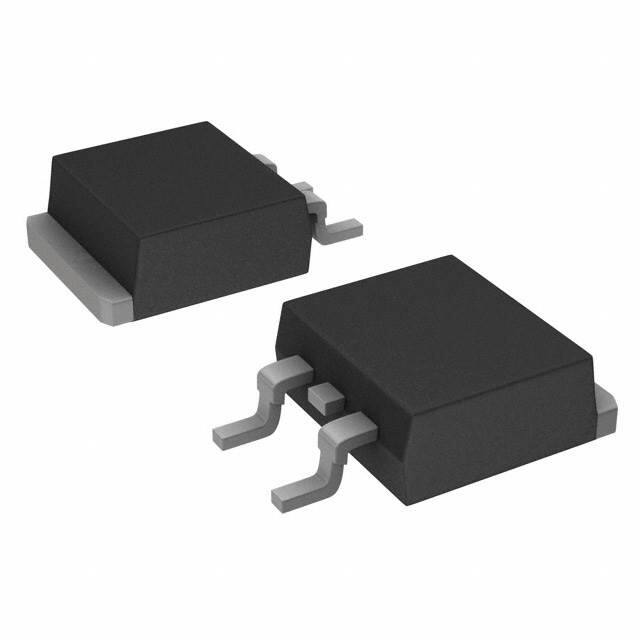
D²PAK
•
•
•
•
•
•
AEC-Q101 qualified revision C
PPAP capable
High junction temperature capability
Low leakage current
Low thermal resistance
High frequency operation
•
ECOPACK®2 compliant
Applications
•
•
Switching mode power supply
Automotive DC/DC converter
Description
Dual center tab Schottky rectifier suited for high frequency switched mode power
supplies.
Product status links
STPS40150C-Y
Product summary
IF(AV)
2 x 20 A
VRRM
150 V
Tj(max.)
175 °C
VF(typ.)
0.69 V
DS12474 - Rev 3 - December 2018
For further information contact your local STMicroelectronics sales office.
www.st.com
�STPS40150C-Y
Characteristics
1
Characteristics
Table 1. Absolute ratings (limiting values, per diode at 25 °C, unless otherwise specified)
Symbol
Parameter
VRRM
Repetitive peak reverse voltage
IF(RMS)
Forward rms current
Tj from -40 °C to 175 °C
Value
Unit
150
V
60
A
TC = 150 °C
Per diode
20
TC = 145 °C
Per device
40
IF(AV)
Average forward current, δ = 0.5, square wave
IFSM
Surge non repetitive forward current
tp = 10 ms sinusoidal
250
A
PARM
Repetitive peak avalanche power
tp = 10 µs, Tj = 125 °C
1080
W
Storage temperature range
-65 to +175
°C
Operating junction temperature(1)
-40 to +175
°C
Tstg
Tj
A
1. (dPtot/dTj) < (1/Rth(j-a)) condition to avoid thermal runaway for a diode on its own heatsink.
Table 2. Thermal parameters
Symbol
Value
Parameter
Rth(j-c)
Junction to case
Rth(c)
Coupling
Unit
Max.
Per diode
1.2
Total
0.85
°C/W
0.5
°C/W
When the diodes 1 and 2 are used simultaneously:
ΔTj (diode1) = P(diode1) x Rth(j-c) (per diode) + P(diode2) x Rth(c)
Table 3. Static electrical characteristics (per diode)
Symbol
IR
Parameter
Reverse leakage current
Test conditions
Tj = 25 °C
Tj = 125 °C
Tj = 25 °C
VF
Forward voltage drop
Tj = 125 °C
Tj = 25 °C
Tj = 125 °C
VR = VRRM
IF = 20 A
IF = 40 A
Min.
Typ.
-
4
-
Unit
15
µA
17
mA
0.92
0.69
-
Max.
0.75
1.00
0.79
V
0.86
1. Pulse test: tp = 5 ms, δ < 2%
2. Pulse test: tp =380 µs, δ < 2%
To evaluate the conduction losses, use the following equation:
P = 0.64 x IF(AV) + 0.0055 x IF 2 (RMS)
DS12474 - Rev 3
page 2/9
�STPS40150C-Y
Characteristics (curves)
1.1
Characteristics (curves)
Figure 1. Average forward power dissipation versus
average forward current (per diode)
22
PF(AV)(W)
δ=0.1
δ=0.05
20
δ=0.2
Figure 2. Average forward current versus ambient
temperature (δ = 0.5, per diode)
50
δ=0.5
IF(AV) (A)
45
18
δ=1.0
16
Rth(j-a)=Rth(j-c)
40
35
14
30
12
25
10
20
8
6
15
T
4
T
10
2
δ=tp/T
0
0
2
4
6
8
10
12
14
16
IF(AV) (A)
tp
18
20
22
24
26
5
28
Figure 3. Relative variation of thermal impedance junction
to case versus pulse duration
δ=tp/T
tp
Tamb (°C)
0
0
25
50
75
100
125
150
175
Figure 4. Reverse leakage current versus reverse voltage
applied (typical values, per diode)
I R (µA)
Z th(j-c) / R th(j-c)
1.E+05
1.0
0.9
Tj = 150 °C
1.E+04
0.8
Tj = 125 °C
0.7
1.E+03
Tj = 100 °C
0.6
1.E+02
0.5
0.4
Tj = 75 °C
Tj = 50 °C
1.E+01
0.3
Tj = 25 °C
1.E+00
0.2
0.1
0.0
1.E-05
VR(V)
t p(s)
Single pulse
1.E-01
0
1.E-04
1.E-03
1.E-02
1.E-01
10
20
30
40
50
60
70
80
90 100 110 120 130 140 150
1.E+00
Figure 5. Junction capacitance versus reverse voltage
applied (typical values, per diode)
C(pF)
Figure 6. Forward voltage drop versus forward current
(typical values, per diode)
1000.0
1000
I F (A)
F = 1 MHz
VOSC = 30 mVRMS
Tj = 25 °C
100.0
Tj = 75 °C
Tj = 125 °C
10.0
100
Tj = 25 °C
1.0
VF(V)
VR(V)
0.1
10
1
DS12474 - Rev 3
10
100
1000
0.0
0.2
0.4
0.6
0.8
1.0
1.2
1.4
1.6
page 3/9
�STPS40150C-Y
Characteristics (curves)
Figure 7. Thermal resistance junction to ambient versus
copper surface under tab (typical values, epoxy printed
board FR4, eCu = 35 µm)
80
Figure 8. Normalized avalanche power derating versus
pulse duration (Tj = 125 °C)
Rth(j-a) (°C/W)
1
D²PAK
70
PARM (t p )
PARM (10 µs)
Epoxy printed board FR4, copper thickness = 35 µm
60
0.1
50
40
30
0.01
20
10
SCu (cm²)
0.001
0
0
5
DS12474 - Rev 3
10
15
20
25
30
35
40
t p(µs)
1
10
100
1000
page 4/9
�STPS40150C-Y
Package information
2
Package information
In order to meet environmental requirements, ST offers these devices in different grades of ECOPACK®
packages, depending on their level of environmental compliance. ECOPACK® specifications, grade definitions
and product status are available at: www.st.com. ECOPACK® is an ST trademark.
2.1
D²PAK package information
•
•
Epoxy meets UL94, V0.
Cooling method: by conduction (C)
Figure 9. D²PAK package outline
Note:
DS12474 - Rev 3
This package drawing may slightly differ from the physical package. However, all the specified dimensions are
guaranteed.
page 5/9
�STPS40150C-Y
D²PAK package information
Table 4. D²PAK package mechanical data
Dimensions
Ref.
Millimeters
Min.
Typ.
Inches (for reference only)
Max.
Min.
Typ.
Max.
A
4.40
4.60
0.173
0.181
A1
0.03
0.23
0.001
0.009
b
0.70
0.93
0.028
0.037
b2
1.14
1.70
0.045
0.067
c
0.45
0.60
0.018
0.024
c2
1.23
1.36
0.048
0.053
D
8.95
9.35
0.352
0.368
D1
7.50
7.75
8.00
0.295
0.305
0.315
D2
1.10
1.30
1.50
0.043
0.051
0.060
E
10.00
10.40
0.394
E1
8.30
8.50
8.70
0.335
0.343
0.346
E2
6.85
7.05
7.25
0.266
0.278
0.282
e
0.409
2.54
0.100
e1
4.88
5.28
0.190
0.205
H
15.00
15.85
0.591
0.624
J1
2.49
2.69
0.097
0.106
L
2.29
2.79
0.090
0.110
L1
1.27
1.40
0.049
0.055
L2
1.30
1.75
0.050
0.069
R
V2
0.40
0°
0.015
8°
0°
8°
Figure 10. D²PAK recommended footprint (dimensions are in mm)
Footprint
DS12474 - Rev 3
page 6/9
�STPS40150C-Y
Ordering information
3
Ordering information
Table 5. Order code
DS12474 - Rev 3
Order code
Marking
Package
Weight
Base qty.
Delivery mode
STPS40150CGY-TR
STPS40150CGY
D²PAK
1.48 G
1000
Tape and reel
page 7/9
�STPS40150C-Y
Revision history
Table 6. Document revision history
DS12474 - Rev 3
Date
Revision
Changes
12-Mar-2018
1
First issue.
07-Dec-2018
2
Added Figure 8. Updated Table 1.
12-Dec-2018
3
Updated Table 3.
page 8/9
�STPS40150C-Y
IMPORTANT NOTICE – PLEASE READ CAREFULLY
STMicroelectronics NV and its subsidiaries (“ST”) reserve the right to make changes, corrections, enhancements, modifications, and improvements to ST
products and/or to this document at any time without notice. Purchasers should obtain the latest relevant information on ST products before placing orders. ST
products are sold pursuant to ST’s terms and conditions of sale in place at the time of order acknowledgement.
Purchasers are solely responsible for the choice, selection, and use of ST products and ST assumes no liability for application assistance or the design of
Purchasers’ products.
No license, express or implied, to any intellectual property right is granted by ST herein.
Resale of ST products with provisions different from the information set forth herein shall void any warranty granted by ST for such product.
ST and the ST logo are trademarks of ST. All other product or service names are the property of their respective owners.
Information in this document supersedes and replaces information previously supplied in any prior versions of this document.
© 2018 STMicroelectronics – All rights reserved
DS12474 - Rev 3
page 9/9
�
很抱歉,暂时无法提供与“STPS40150CGY-TR”相匹配的价格&库存,您可以联系我们找货
免费人工找货